


RICHTEK RT9161B-41CG, RT9161B-41CX, RT9161B-42CG, RT9161B-42CX, RT9161B-43CG Datasheet
...
Preliminary
RT9161B
Simple Lithium-Ion Battery Charger
General Description
The RT9161B is a single-cell lithium-ion battery
charger. It includes an on-chip pass transistor for
high precision charging. Featuring with ultrahigh
precision (±1%), the RT9161B provides a very
effective and low cost solution for charging lithium-
ion battery.
Other features of the RT9161B are current limit and
thermal shutdown protection. The output voltage of
RT9161B is internally set and ranges from 4.10V to
4.35V, in 0.05V steps. The RT9161B comes in the
SOT-89 and SOT-223 packages.
Ordering Information
RT9161B-
Package type
X : SOT-89
G : SOT-223
Operating temperature range
C: Commercial standard
Output voltage
41 : 4.10V
4A : 4.15V
42 : 4.20V
4B : 4.25V
43 : 4.30V
4C : 4.35V
Features
z
High Accuracy Charge Voltage: ±±±±1%
z
6 Available Output Voltages
z
Low 450mV Dropout at 300mA
z
Wide Input Voltage Range
z
Thermal Shutdown and Current Limit Protection
z
SOT-89 and SOT-223
z
Low Ground Current 110µµµµA
Applications
z Li-Ion Battery Charger
z Cellular Phones
z Palmtop Computers
z PDAs
z Self Charging Battery Packs
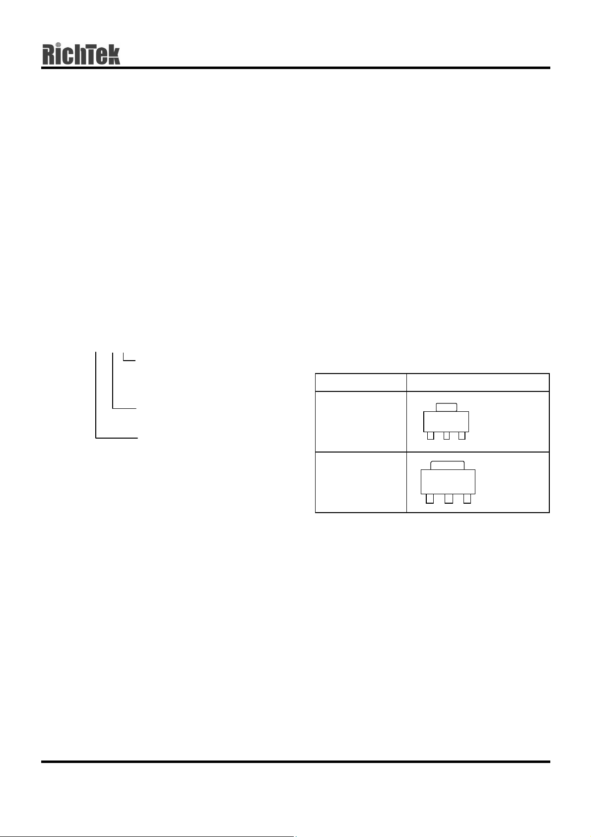
Pin Configurations
Part Number Pin Configurations
RT9161B-CX
(Plastic SOT-89)
123
RT9161B-CG
(Plastic SOT-223)
123
TOP VIEW
1. GND
2. VIN (TAB)
3. VOUT
TOP VIEW
1. GND
2. VIN (TAB)
3. VOUT
DS9161B-02 April 2001 www.richtek-ic.com.tw
1
RT9161B
Preliminary
Absolute Maximum Ratings
z Input Voltage -0.3 ~ 14V
z Power Dissipation, P
@ TA = 25°C
D
SOT-89 0.5W
• Package Thermal Resistance
SOT-89, θ
SOT-89, θ
SOT-223, θ
SOT-223, θ
z Operating Junction Temperature Range -40°C ~ 125°C
z Storage Temperature Range -65°C ~ 150°C
JC
JA
JC
JA
100°C/W
300°C/W
15°C/W
60°C/W
Electrical Characteristics
(TA = 25°C, CIN = 1µF, C
= 10µF, unless otherwise specified)
OUT
Parameter Symbol Test Conditions Min Typ Max Units
Input Voltage Range
(1)
Output Voltage Accuracy
Output Voltage Temperature
Coefficient
(1)
Line Regulation
Load Regulation
Current Limit
Dropout Voltage
(2)
(3)
(4)
Standby Current
V
IN
∆V
OUT
∆V
LINE
∆V
LOAD
I
LIMIT
V
DROP
I
STANDBY
IL = 1mA, VIN = 5V
IL = 1mA, VIN = 4.5 ~ 12 V
IL = 1mA ~ 300/500/mA, , VIN = 5V
VIN = 5V, V
OUT
= 0V
IL = 300/500mA -- 450/750 -- mV
IL = 0, VIN = 12V
4.5 -- 14 V
-1 -- +1 %
-- 50 150
-- 2 3 %V
-- 1 30/50 mV
300 -- 600 mA
-- 110 180
Note:
(1) Guaranteed by design.
(2) Regulation is measured at constant junction temperature, using pulsed ON time.
(3) Current Limit is measured at constant junction temperature, using pulsed ON time.
(4) Dropout is measured at constant junction temperature, using pulsed ON time.
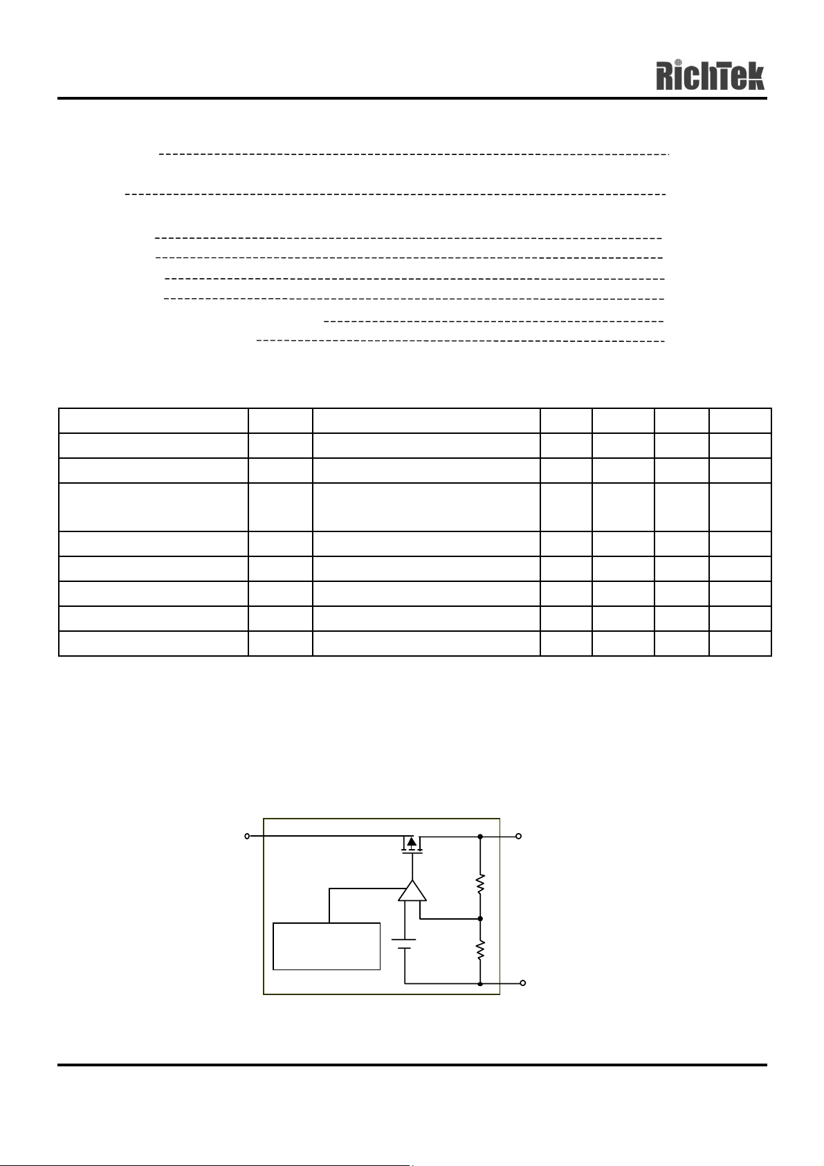
Function Block Diagram
PPM/°C
OUT
µA
VIN
Error
_
+
Amp
Current Limit
Thermal
Shutdown
www.richtek-ic.com.tw DS9161B-02 April 2001
1.2V
Reference
VOUT
GND
2
 Loading...