

®
3A, 1MHz, Synchronous Step-Down Converter
RT8068A
General Description
The RT8068A is a high efficiency synchronous, step-down
DC/DC converter. It's input voltage range from 2.7V to 5.5V
that provides an adjustable regulated output voltage from
0.6V to V
while delivering up to 3A of output current.
IN
The internal synchronous low on resistance power
switches increase efficiency and eliminate the need for
an external Schottky diode. The switching frequency is
fixed internally at 1MHz. The 100% duty cycle provides
low dropout operation, hence extending battery life in
portable systems. Current mode operation with internal
compensation allows the transient response to be
optimized over a wide range of loads and output capacitors.
The RT8068A is available in WDFN-10L 3x3 and SOP-8
(Exposed Pad) packages.
Ordering Information
RT8068A
Package Type
QW : WDFN-10L 3x3 (W-Type)
SP :
SOP-8 (Exposed Pad-Option 2)
Lead Plating System
Z : ECO (Ecological Element with
Halogen Free and Pb free)
Note :
Richtek products are :
RoHS compliant and compatible with the current require-
ments of IPC/JEDEC J-STD-020.
Suitable for use in SnPb or Pb-free soldering processes.
Marking Information
RT8068AZQW
13 : Product Code
13 YM
DNN
YMDNN : Date Code
Features
High Efficiency : Up to 95%
Low R
Internal Switches : 69m
DS(ON)
ΩΩ
Ω/49m
ΩΩ
= 5V
Fixed Frequency : 1MHz
No Schottky Diode Required
Internal Compensation
0.6V Reference Allows Low Output Voltage
Low Dropout Operation : 100% Duty Cycle
OCP, UVP, OVP, OTP
RoHS Compliant and Halogen Free
Applications
Portable Instruments
Battery Powered Equipment
Notebook Computers
Distrib uted Power Systems
IP Phones
Digital Cameras
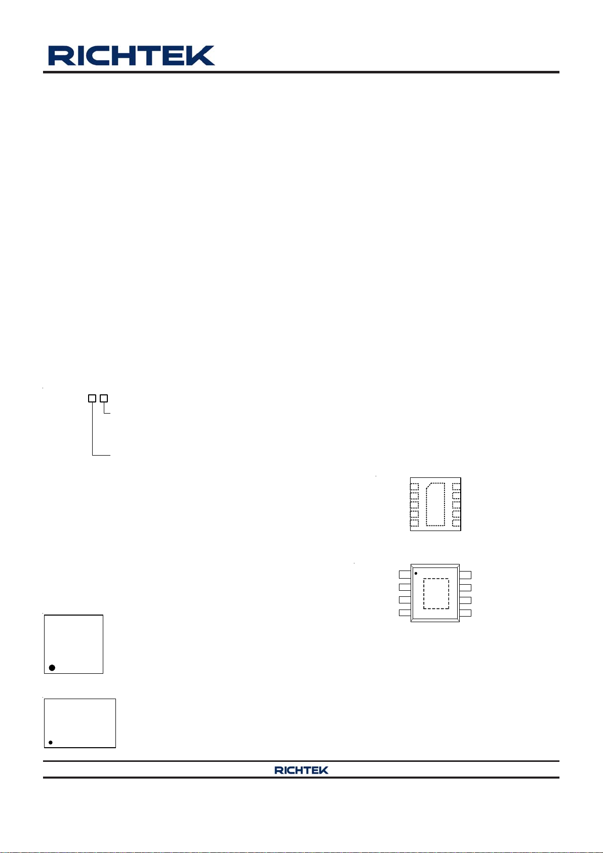
Pin Configurations
(TOP VIEW)
GND
GND
11
9
10
PVIN
9
PVIN
8
SVIN
7
NC
6
FB
8
PVIN
7
PVIN
6
SVIN
5
FB
1
LX
2
LX
3
LX
EN
4
5
PGOOD
WDFN-10L 3x3
LX
2
LX
PGOOD
EN
3
4
SOP-8 (Exposed Pad)
ΩΩ
Ω at V
ΩΩ
IN
RT8068AZSP
RT8068AZSP : Product Code
RT8068A
YMDNN : Date Code
ZSPYMDNN
Copyright 2015 Richtek Technology Corporation. All rights reserved. is a registered trademark of Richtek Technology Corporation.
DS8068A-05 June 2015 www.richtek.com
©
1

RT8068A
Typical Application Circuit
PGOOD
V
IN
Chip Enable
R1
100k
C
10µF
RT8068A
PGOOD
PVIN
IN
C1
1µF
SVIN
EN
LX
FB
GND
L
C
OUT
C
R
FB1
R
FB2
FF
Table 1. Recommended Component Selection
V
(V) R
OUT
(k) R
FB1
(k) C
FB2
(pF) L (H) C
FF
3.3 229.5 51 22 2 22 x 2
2.5 161.5 51 22 2 22 x 2
1.8 102 51 22 1.5 22 x 2
1.5 76.5 51 22 1.5 22 x 2
1.2 51 51 22 1.5 22 x 2
1.0 34 51 22 1.5 22 x 2
OUT
V
OUT
(F)
Functional Pin Description
Pin No.
WDFN-10L
SOP-8
(Exposed Pad)
1, 2, 3 1, 2 LX Switch Node. Connect this pin to the induc tor.
4 3 PGOOD
5 4 EN Enable Contro l. P ull high to turn on. Do not fl oat.
6 5 FB
7 -- NC No Internal Connection.
8 6 SVIN
9,10 7,8 PVI N
11
(Exposed Pad)
(Exposed Pad)
9
Pin
Name
GND
Pin Function
Power Good Indicator. This pin is an open drain logic output that is
pulled to ground when the output voltage is less than 90 % of the
target output voltage. Hysteresis = 5%.
Feedback Pin. Th is pin receives the feedback voltage from a
resistive voltage divider connected ac ross the output.
Signal Input Pin. Decouple th is pin to GND wit h a t least 1F ceramic
cap.
Power Input Pin. Decouple this pin to GND with at least 4.7F
ceramic cap.
Ground. The exposed pa d must be soldered t o a large PCB and
connected to GND for maximum power dissipation.
Copyright 2015 Richtek Technology Corporation. All rights reserved. is a registered trademark of Richtek Technology Corporation.
2
©
DS8068A-05 June 2015www.richtek.com

Function Block Diagram
RT8068A
EN
PGOOD
FB
PGOOD
V
REF
0.6V
EA
POR
SVIN
Int-SS
EN
Output
Clamp
0.72V
0.54V
0.4V
OSC
OV
PGOOD
UV
Slope
Com
Control
Logic
OTP
ISEN
OC
Limit
PVIN
Driver
LX
NISEN
Zero Current
100
Copyright 2015 Richtek Technology Corporation. All rights reserved. is a registered trademark of Richtek Technology Corporation.
©
DS8068A-05 June 2015 www.richtek.com
3

RT8068A
Absolute Maximum Ratings (Note 1)
Supply Input Voltage, PVIN, SVIN ------------------------------------------------------------------------------------- −0.3V to 6.5V
LX Pin
DC----------------------------------------------------------------------------------------------------------------------------- −0.3V to 6.8V
< 20ns ----------------------------------------------------------------------------------------------------------------------- −2.5V to 9V
Other I/O Pin Voltage ----------------------------------------------------------------------------------------------------- −0.3V to 6.5V
Power Dissipation, P
WDFN-10L 3x3 ------------------------------------------------------------------------------------------------------------- 1.429W
SOP-8 (Exposed Pad) --------------------------------------------------------------------------------------------------- 1.333W
Package Thermal Resistance (Note 2)
WDFN-10L 3x3, θJA------------------------------------------------------------------------------------------------------- 70°C/W
WDFN-10L 3x3, θJC------------------------------------------------------------------------------------------------------- 8.2°C/W
SOP-8 (Exposed Pad), θJA---------------------------------------------------------------------------------------------- 75°C/W
SOP-8 (Exposed Pad), θJC--------------------------------------------------------------------------------------------- 15°C/W
Lead Temperature (Soldering, 10 sec.) ------------------------------------------------------------------------------- 260°C
Junction Temperature ----------------------------------------------------------------------------------------------------- 150°C
Storage Temperature Range -------------------------------------------------------------------------------------------- −65°C to 150°C
ESD Susceptibility (Note 3)
HBM (Human Body Model)---------------------------------------------------------------------------------------------- 2kV
MM (Machine Model) ----------------------------------------------------------------------------------------------------- 200V
@ TA = 25°C
D
Recommended Operating Conditions
Supply Input Voltage, PVIN, SVIN ------------------------------------------------------------------------------------- 2.7V to 5.5V
Junction Temperature Range -------------------------------------------------------------------------------------------- −40°C to 125°C
Ambient Temperature Range -------------------------------------------------------------------------------------------- −40°C to 85°C
(Note 4)
Electrical Characteristics
(VIN = 3.3V, T
Feedback Reference Voltage V
Feedback Leakage Current IFB -- 0.1 0.4 A
DC Bias Current
Output Voltage Line Regulation
Output Voltage Load Regulation I
Switch Leakage Current -- -- 1 A
Switching Frequency 0.8 1 1.2 MHz
Switch On Resistance, High R
Switch On Resistance, Low R
P-MOSFET Current Limit I
Copyright 2015 Richtek Technology Corporation. All rights reserved. is a registered trademark of Richtek Technology Corporation.
4
©
= 25°C, unless otherwise specified)
A
Parameter Symbol Test Conditions Min Typ Max Unit
0.594 0.6 0.606 V
REF
Active , V
Switching
= 0.7V, Not
FB
-- 110 140
A
Shutdown -- -- 1
= 2.7V to 5.5V
V
IN
I
= 0A
OUT
= 0A to 3A 1 -- 1 %
OUT
DS(ON)_P
DS(ON)_N
LIM
VIN = 5V -- 69 -- m
VIN = 5V -- 49 -- m
4 -- -- A
-- 0.3 -- %/V
DS8068A-05 June 2015www.richtek.com

Parameter Symbol Test Conditions Min Typ Max Unit
Under Voltage Lockout
Threshold
V
UVLO
RT8068A
Rising 2.2 2.4 2.6
V
IN
VIN Falling 2 2.2 2.4
V
EN Input
Threshold Voltage
Logic-High V
Logic-Low VIL -- -- 0.4
1.6 -- --
IH
V
EN Pull Low Resistance -- 500 -- k
Over Temperature Protection TSD -- 150 -- C
Over Temperature Protection
Hysteresis
-- 20 -- C
Soft-Start Time tSS 500 -- -- s
V
Discharge Resistance -- 100 --
OUT
V
Over Voltage Protection
OUT
(Latch-Off, Delay Time = 10s)
V
Under Voltage Lock Out
OUT
(Latch-Off)
Power Good
115 120 130 %
57 66 75 %
Measured FB, With Respect to
V
REF
85 90 -- %
Power Good Hysteresis -- 5 -- %
Note 1. Stresses beyond those listed “Absolute Maximum Ratings” may cause permanent damage to the device. These are
stress ratings only, and functional operation of the device at these or any other conditions beyond those indicated in
the operational sections of the specifications is not implied. Exposure to absolute maximum rating conditions may
affect device reliability.
Note 2. θ
Note 3. Devices are ESD sensitive. Handling precaution is recommended.
Note 4. The device is not guaranteed to function outside its operating conditions.
is measured at T
JA
measured at the exposed pad of the package.
= 25°C on a high effective thermal conductivity four-layer test board per JEDEC 51-7. θJC is
A
Copyright 2015 Richtek Technology Corporation. All rights reserved. is a registered trademark of Richtek Technology Corporation.
DS8068A-05 June 2015 www.richtek.com
©
5

RT8068A
Typical Operating Characteristics
Efficiency vs. Load Current
100
90
VIN = 4.2V
V
= 5V
IN
80
70
60
50
40
Efficiency (%)
30
20
10
0
0 0.5 1 1.5 2 2.5 3
V
OUT
= 3.3V
Load Current (A)
Efficiency vs. Load Current
100
90
VIN = 3.3V
80
70
60
50
40
Efficiency (%)
30
20
10
= 5V
V
IN
V
= 1.05V
0
00.511.522.5 3
OUT
Load Current (A)
Output Voltage (V)
Efficiency vs. Load Current
100
90
VIN = 3.3V
80
V
= 5V
IN
70
60
50
40
Efficiency (%)
30
20
10
0
00.511.522.5 3
V
OUT
Load Current (A)
Output Voltage vs. Output Current
1.820
1.815
1.810
1.805
1.800
1.795
1.790
1.785
1.780
VIN = 5V
VIN = 3.3V
V
OUT
0 0.5 1 1.5 2 2.5 3
Output Current (A)
= 1.8V
= 1.8V
Current Limit vs. Input Voltage
7.0
6.5
6.0
5.5
5.0
4.5
Current Limit (A)
4.0
3.5
3.0
2.533.544.555.5
V
OUT
= 1.05V
Input Voltage (V)
Copyright 2015 Richtek Technology Corporation. All rights reserved. is a registered trademark of Richtek Technology Corporation.
©
7.0
6.5
6.0
5.5
5.0
4.5
Current Limit (A)
4.0
3.5
3.0
Current Limit vs. Temperature
VIN = 5V
VIN = 3.3V
V
= 1.05V
OUT
-50 -25 0 25 50 75 100 125
Temperature (°C)
DS8068A-05 June 2015www.richtek.com
6

RT8068A
90
85
80
75
70
Ω
65
(mΩ )
60
DS(ON)
55
R
50
45
40
35
V
OUT
(50mV/Div)
R
-50 -25 0 25 50 75 100 125
vs. Temperature
DS(ON)
P-MOSFET
N-MOSFET
VIN = 5V
Temperature (°C)
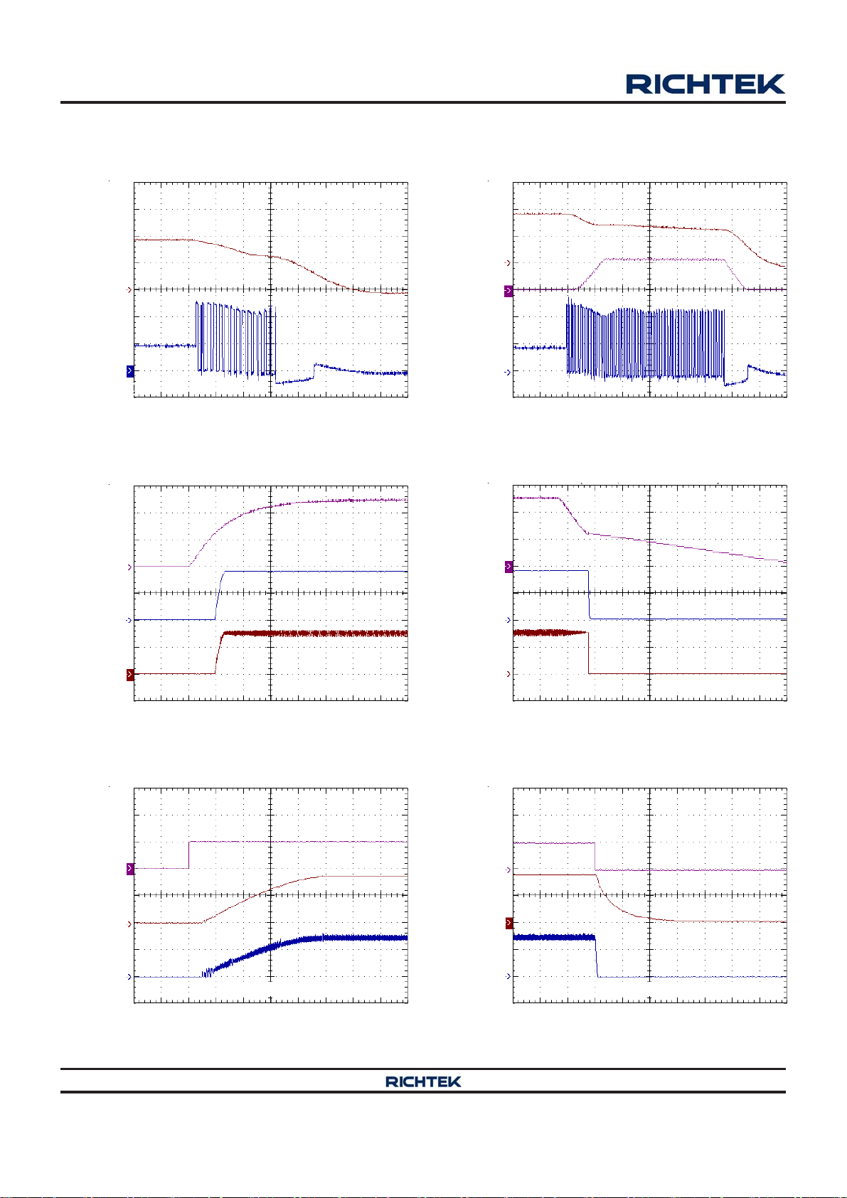
Load Transient Response
V
OUT
(50mV/Div)
I
OUT
(2A/Div)
V
OUT
(5mV/Div)
Load Transient Response
VIN = 5V, V
= 1.8V, I
OUT
Time (50μs/Div)
= 0.5A to 3A
OUT
Switching
I
OUT
(2A/Div)
V
OUT
(5mV/Div)
V
LX
(5V/Div)
I
LX
(2A/Div)
VIN = 5V, V
Time (50μs/Div)
Switching
VIN = 5V, V
= 1.8V, I
OUT
OUT
= 1.5A to 3A
OUT
= 1.8V, I
OUT
= 3A
V
LX
(5V/Div)
I
LX
(1A/Div)
V
OUT
(1V/Div)
V
LX
(2V/Div)
VIN = 5V, V
= 1.8V, I
OUT
OUT
Time (500ns/Div)
Over Voltage Protection
VIN = 5V, V
= 1.8V, I
OUT
= 1.5A
OUT
= 1A
Time (500ns/Div)
Copyright 2015 Richtek Technology Corporation. All rights reserved. is a registered trademark of Richtek Technology Corporation.
©
Time (10μs/Div)
DS8068A-05 June 2015 www.richtek.com
7
RT8068A
V
OUT
(1V/Div)
V
LX
(2V/Div)
V
IN
(2V/Div)
Under Voltage Protection
VIN = 5V, V
Time (5μs/Div)
Power On from V
OUT
IN
= 1.8V
V
OUT
(1V/Div)
I
LX
(5A/Div)
V
LX
(2V/Div)
V
IN
(2V/Div)
Over Current Protection
VIN = 5V, V
Time (2.5μs/Div)
Power Off from V
OUT
IN
= 1.8V
V
OUT
(1V/Div)
I
LX
(2A/Div)
V
EN
(5V/Div)
V
OUT
(1V/Div)
I
LX
(2A/Div)
V
= 1.8V, I
OUT
Time (2.5ms/Div)
Power On from EN
VIN = 5V, V
Time (200μs/Div)
= 1.8V, I
OUT
OUT
OUT
= 3A
= 3A
V
OUT
(1V/Div)
I
LX
(2A/Div)
V
EN
(5V/Div)
V
OUT
(1V/Div)
I
LX
(2A/Div)
V
= 1.8V, I
OUT
Time (2.5ms/Div)
Power Off from EN
VIN = 5V, V
Time (40μs/Div)
= 1.8V, I
OUT
OUT
OUT
= 3A
= 3A
Copyright 2015 Richtek Technology Corporation. All rights reserved. is a registered trademark of Richtek Technology Corporation.
©
DS8068A-05 June 2015www.richtek.com
8

Application Information
RT8068A
The RT8068A is a single-phase buck converter. It provides
single feedback loop, current mode control with fast
transient response. An internal 0.6V reference allows the
output voltage to be precisely regulated for low output
voltage applications. A fixed switching frequency (1MHz)
oscillator and internal compensation are integrated to
minimize external component count. Protection features
include over current protection, under voltage protection,
over voltage protection and over temperature protection.
Output Voltage Setting
Connect a resistive voltage divider at the FB between V
OUT
and GND to adjust the output voltage. The output voltage
is set according to the following equation :
R
V = V 1 +
OUT REF
where V
is 0.6V (typ.).
REF
Figure 1. Setting V
FB1
R
FB2
GND
V
OUT
R
FB1
FB
R
FB2
with a Voltage Divider
OUT
Chip Enable and Disable
The EN pin allows for power sequencing between the
controller bias voltage and another voltage rail. The
RT8068A remains in shutdown if the EN pin is lower than
400mV. When the EN pin rises above the VEN trip point,
the RT8068A begins a new initialization and soft-start cycle.
UVLO Protection
The RT8068A has input Under Voltage Lockout protection
(UVLO). If the input voltage exceeds the UVLO rising
threshold voltage (2.4V typ.), the converter resets and
prepares the PWM for operation. If the input voltage falls
below the UVLO falling threshold voltage during normal
operation, the device will stop switching. The UVLO rising
and falling threshold voltage has a hysteresis to prevent
noise-caused reset.
Inductor Selection
The switching frequency (on-time) and operating point (%
ripple or LIR) determine the inductor value as shown below:
VV V
L =
OUT IN OUT
f LIR I V
SW LOAD(MAX) IN
where LIR is the ratio of the peak-to-peak ripple current to
the average inductor current.
Find a low loss inductor having the lowest possible DC
resistance that fits in the allotted dimensions. Ferrite cores
are often the best choice, although powdered iron is
inexpensive and can work well at 200kHz. The core must
be large enough not to saturate at the peak inductor current
(I
) :
PEAK
LIR
I = I + I
PEAK LOAD(MAX) LOAD(MAX)
2
The calculation above serves as a general reference. To
further improve transient response, the output inductor
can be further reduced. This relation should be considered
along with the selection of the output capacitor.
Internal Soft-Start
The RT8068A provides an internal soft-start function to
prevent large inrush current and output voltage overshoot
when the converter starts up. The soft-start (SS)
automatically begins once the chip is enabled. During soft-
start, the internal soft-start capacitor becomes charged
and generates a linear ramping up voltage across the
Input Capacitor Selection
High quality ceramic input decoupling capacitor, such as
X5R or X7R, with values greater than 20μF are
recommended for the input capacitor. The X5R and X7R
ceramic capacitors are usually selected for power regulator
capacitors because the dielectric material has less
capacitance variation and more temperature stability.
capacitor. This voltage clamps the voltage at the FB pin,
causing PWM pulse width to increase slowly and in turn
reduce the output surge current. The internal 0.6V
reference takes over the loop control once the internal
ramping-up voltage becomes higher than 0.6V.
Copyright 2015 Richtek Technology Corporation. All rights reserved. is a registered trademark of Richtek Technology Corporation.
DS8068A-05 June 2015 www.richtek.com
©
Voltage rating and current rating are the key parameters
when selecting an input capacitor. Generally, selecting an
input capacitor with voltage rating 1.5 times greater than
the maximum input voltage is a conservatively safe design.
9

RT8068A
The input capacitor is used to supply the input RMS
current, which can be approximately calculated using the
following equation :
I = I 1
IN_RMS LOAD
VV
OUT OUT
VV
IN IN
The next step is selecting a proper capacitor for RMS
current rating. One good design is using more than one
capacitor with low equivalent series resistance (ESR) in
parallel to form a capacitor bank.
The input capacitance value determines the input ripple
voltage of the regulator. The input voltage ripple can be
approximately calculated using the following equation :
I0.25
IN
OUT(MAX)
V =
For example, if I
Cf
IN SW
OUT_MAX
= 3A, CIN = 20μF, fSW = 1MHz,
the input voltage ripple will be 37.5mV.
Output Capacitor Selection
The output capacitor and the inductor form a low pass
filter in the buck topology. In steady state condition, the
ripple current flowing into/out of the capacitor results in
ripple voltage. The output voltage ripple (V
) can be
P-P
calculated by the following equation :
V= LIRI ESR +
P_P LOAD(MAX)
1
8C f
OUT SW
When load transient occurs, the output capacitor supplies
the load current before the controller can respond.
Therefore, the ESR will dominate the output voltage sag
during load transient. The output voltage undershoot (V
SAG
can be calculated by the following equation :
V = I ESR
SAG LOAD
For a given output voltage sag specification, the ESR value
can be determined.
Another parameter that has influence on the output voltage
sag is the equivalent series inductance (ESL). The rapid
change in load current results in di/dt during transient.
Therefore, the ESL contributes to part of the voltage sag.
Using a capacitor with low ESL can obtain better transient
performance. Generally, using several capacitors
connected in parallel can have better transient performance
than using a single capacitor for the same total ESR.
Unlike the electrolytic capacitor, the ceramic capacitor has
relatively low ESR and can reduce the voltage deviation
during load transient. However, the ceramic capacitor can
only provide low capacitance value. Therefore, use a mixed
combination of electrolytic capacitor and ceramic capacitor
to obtain better transient performance.
Power Good Output (PGOOD)
PGOOD is an open-drain type output and requires a pull-
up resistor. PGOOD is actively held low in soft-start,
standby, and shutdown. It is released when the output
voltage rises above 90% of nominal regulation point. The
PGOOD signal goes low if the output is turned off or is
10% below its nominal regulation point.
Under Voltage Protection (UVP)
The output voltage can be continuously monitored for under
voltage. When under voltage protection is enabled, both
UGATE and LGATE gate drivers will be forced low if the
output is less than 66% of its set voltage threshold. The
UVP will be ignored for at least 3ms (typ.) after start up or
a rising edge on the EN threshold. Toggle EN threshold or
cycle VIN to reset the UVP fault latch and restart the
controller.
Over Voltage Protection (OVP)
The RT8068A is latched once OVP is triggered and can
only be released by toggling EN threshold or cycling VIN.
There is a 10μs delay built into the over voltage protection
circuit to prevent false transition.
)
Over Current Protection (OCP)
The RT8068A provides over current protection by detecting
high side MOSFET peak inductor current. If the sensed
peak inductor current is over the current limit threshold
(4A typ.), the OCP will be triggered. When OCP is tripped,
the RT8068A will keep the over current threshold level
until the over current condition is removed.
Internal Output Voltage Discharge
An internal open-drain logic output is implemented on LX
pin. During the conditions of OVP, UVP, OTP and enable
low, the internal discharge path is activated and the left
energy from output terminal is able to be released with an
internal resistance about 100Ω to ground.
Copyright 2015 Richtek Technology Corporation. All rights reserved. is a registered trademark of Richtek Technology Corporation.
10
©
DS8068A-05 June 2015www.richtek.com

RT8068A
Thermal Shutdown (OTP)
The device implements an internal thermal shutdown
function when the junction temperature exceeds 150°C.
The thermal shutdown forces the device to stop switching
when the junction temperature exceeds the thermal
shutdown threshold. Once the die temperature decreases
below the hysteresis of 20°C, the device reinstates the
power up sequence.
Thermal Considerations
For continuous operation, do not exceed absolute
maximum junction temperature. The maximum power
dissipation depends on the thermal resistance of the IC
package, PCB layout, rate of surrounding airflow, and
difference between junction and ambient temperature. The
maximum power dissipation can be calculated by the
following formula :
P
where T
the ambient temperature, and θ
D(MAX)
= (T
J(MAX)
− TA) / θ
J(MAX)
JA
is the maximum junction temperature, T
is the junction to ambient
JA
A
thermal resistance.
1.50
1.40
1.30
1.20
1.10
1.00
0.90
0.80
0.70
0.60
0.50
0.40
0.30
0.20
0.10
Maximum Power Dissipation (W) 1
0.00
SOP-8 (Exposed Pad)
0 25 50 75 100 125
WDFN-10L 3x3
Four-Layer PCB
Ambient Temperature (°C)
Figure 2. Derating Curve of Maximum Power Dissipation
Layout Considerations
Layout is very important in high frequency switching
converter design. The PCB can radiate excessive noise
is
and contribute to converter instability with improper layout.
Certain points must be considered before starting a layout
using the RT8068A.
For recommended operating condition specifications, the
maximum junction temperature is 125°C and TA is the
ambient temperature. The junction to ambient thermal
resistance, θJA, is layout dependent. For SOP-8 (Exposed
Pad) packages, the thermal resistance, θJA, is 75°C/W
on a standard JEDEC 51-7 four-layer thermal test board.
For WDFN-10L 3x3 packages, the thermal resistance, θJA,
is 70°C/W on a standard JEDEC 51-7 four-layer thermal
test board. The maximum power dissipation at T
= 25°C
A
can be calculated by the following formulas :
P
= (125°C − 25°C) / (75°C/W) = 1.333W for
D(MAX)
SOP-8 (Exposed Pad) package
P
= (125°C − 25°C) / (70°C/W) = 1.429W for
D(MAX)
WDFN-10L 3x3 package
The maximum power dissipation depends on the operating
ambient temperature for fixed T
and thermal
J(MAX)
resistance, θJA. For the RT8068A package, the derating
curves in Figure 2 allow the designer to see the effect of
rising ambient temperature on the maximum power
dissipation.
Make the traces of the main current paths as short and
wide as possible.
Put the input capacitor as close as possible to the device
pins (VIN and GND).
LX node encounters high frequency voltage swings so it
should be kept in a small area. Keep sensitive
components away from the LX node to prevent stray
capacitive noise pick-up.
Ensure all feedback network connections are short and
direct. Place the feedback network as close to the chip
as possible.
The GND pin and Exposed Pad should be connected to
a strong ground plane for heat sinking and noise
protection.
An example of PCB layout guide is shown in Figure 3.
for reference.
Copyright 2015 Richtek Technology Corporation. All rights reserved. is a registered trademark of Richtek Technology Corporation.
DS8068A-05 June 2015 www.richtek.com
©
11

RT8068A
The output capacitor must
be placed near the IC.
GND
1
2
3
4
5
V
C
OUT
V
OUT
IN
R
PGOOD
R
LX
LX
LX
PGOOD
EN
EN
LX should be connected to
inductor by wide and short trace.
Keep sensitive components
away from this trace.
Figure 3. PCB Layout Guide
Input capacitor must be placed
as close to the IC as possible.
C
R1
IN1
C
R2
IN2
OUT
V
10
PVIN
9
PVIN
8
SVIN
GND
7
NC
11
6
FB
The voltage divider must
be connected as close to
the device as possible.
Copyright 2015 Richtek Technology Corporation. All rights reserved. is a registered trademark of Richtek Technology Corporation.
©
DS8068A-05 June 2015www.richtek.com
12

Outline Dimension
RT8068A
D
E
A
A3
A1
D2
L
E2
SEE DETAIL A
1
e
b
2
1
1
2
DETAIL A
Pin #1 ID and Tie Bar Mark Options
Note : The configuration of the Pin #1 identifier is optional,
but must be located within the zone indicated.
Dimensions In Millimeters Dimensions In Inches
Symbol
Min Max Min Max
A 0.700 0.800 0.028 0.031
A1 0.000 0.050 0.000 0.002
A3 0.175 0.250 0.007 0.010
b 0.180 0.300 0.007 0.012
D 2.950 3.050 0.116 0.120
D2 2.300 2.650 0.091 0.104
E 2.950 3.050 0.116 0.120
E2 1.500 1.750 0.059 0.069
e 0.500 0.020
L 0.350 0.450
W-Type 10L DFN 3x3 Package
0.014 0.018
Copyright 2015 Richtek Technology Corporation. All rights reserved. is a registered trademark of Richtek Technology Corporation.
DS8068A-05 June 2015 www.richtek.com
©
13

RT8068A
H
EXPOSED THERMAL PAD
(Bottom of Package)
A
Y
J
I
B
X
F
C
D
Dimensions In Millimeters Dimensions In Inches
Symbol
Min Max Min Max
A 4.801 5.004 0.189 0.197
B 3.810 4.000 0.150 0.157
M
C 1.346 1.753 0.053 0.069
D 0.330 0.510 0.013 0.020
F 1.194 1.346 0.047 0.053
H 0.170 0.254 0.007 0.010
I 0.000 0.152 0.000 0.006
J 5.791 6.200 0.228 0.244
M 0.406 1.270 0.016 0.050
X 2.000 2.300 0.079 0.091
Option 1
Y 2.000 2.300 0.079 0.091
X 2.100 2.500 0.083 0.098
Option 2
Y 3.000 3.500 0.118 0.138
8-Lead SOP (Exposed Pad) Plastic Package
Richtek Technology Corporation
14F, No. 8, Tai Yuen 1st Street, Chupei City
Hsinchu, Taiwan, R.O.C.
Tel: (8863)5526789
Richtek products are sold by description only. Richtek reserves the right to change the circuitry and/or specifications without notice at any time. Customers should
obtain the latest relevant information and data sheets before placing orders and should verify that such information is current and complete. Richtek cannot
assume responsibility for use of any circuitry other than circuitry entirely embodied in a Richtek product. Information furnished by Richtek is believed to be
accurate and reliable. However, no responsibility is assumed by Richtek or its subsidiaries for its use; nor for any infringements of patents or other rights of third
parties which may result from its use. No license is granted by implication or otherwise under any patent or patent rights of Richtek or its subsidiaries.
DS8068A-05 June 2015www.richtek.com
14

 Loading...