

1.2A, 24V, 1.4MHz Step-Down Converter
RT8259
General Description
The RT8259 is a high voltage buck converter that can support
the input voltage range from 4.5V to 24V and the output
current can be up to 1.2A. Current Mode operation provides
fast tra nsient response a nd ea ses loop sta bilization.
The chip also provides protection functions such a s cycleby-cycle current limiting and thermal shutdown prote ction.
The RT8259 is available in a SOT-23-6 and TSOT-23-6
pack ages.
Ordering Information
RT8259
Package Type
E : SOT-23-6
J6 : TSOT-23-6
Lead Plating System
G : Green (Halogen Free and Pb Free)
Note :
Richtek products are :
` RoHS compliant and compatible with the current require-
ments of IPC/JEDEC J-STD-020.
` Suitable for use in SnPb or Pb-free soldering processes.
Features
zz
Wide Operating Input Voltage Range : 4.5V to 24V
z
zz
zz
z Adjustable Output Voltage Range : 0.8V to 15V
zz
zz
z 1.2A Output Current
zz
ΩΩ
zz
z 0.3
Ω Internal Power MOSFET Switch
zz
ΩΩ
zz
z High Efficiency up to 92%
zz
zz
z 1.4MHz Fixed Switching Frequency
zz
zz
z Stable with Low ESR Output Ceramic Ca pacitors
zz
zz
z Thermal Shutdown
zz
zz
z Cycle-By-Cycle Over Current Protection
zz
zz
z RoHS Compliant and Halogen Free
zz
Applications
z Distributed Power Systems
z Battery Charger
z Pre-Regulator for Linear Regulators
z WLED Drivers
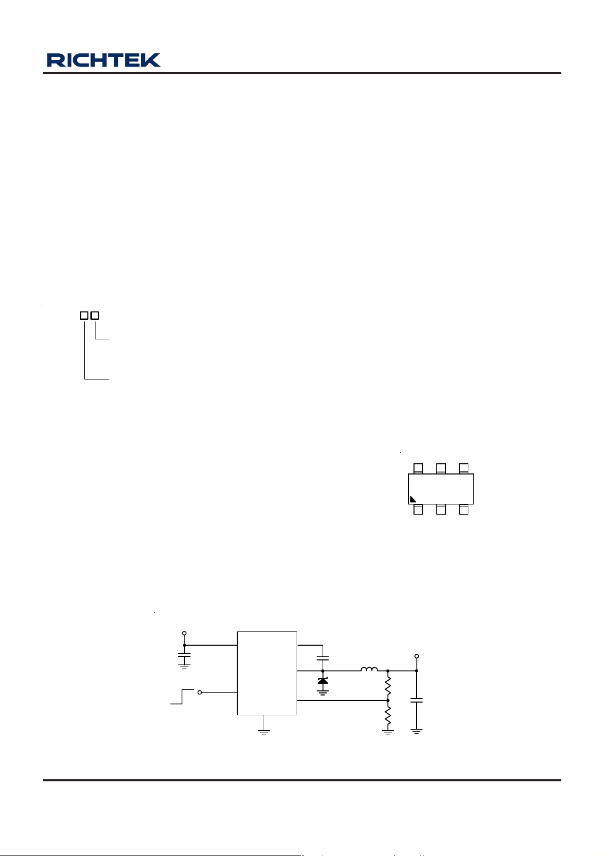
Pin Configurations
(TOP VIEW)
ENVINPHASE
4
56
Marking Information
23
For marking information, conta ct our sales representative
directly or through a Richtek distributor located in your
area.
BOOT GND FB
SOT-23-6/TSOT-23-6
Typical Application Circuit
V
IN
4.5V to 24V
V
R1
62k
R2
19.6k
OUT
3.3V
C2
22µF
C1
10µF
Chip Enabl e
Open =
Automatic Startu p
5
VIN
RT8259
PHASE
4
EN
GND
2
BOOT
FB
1
CB
10nF
6
D1
B230A
3
L1
4.7µH
DS8259-03 March 2011 www.richtek.com
1
RT8259
Table 1. Recommended Component Selection, C2 = 22
V
(V) 1.2 1.8 2.5 3.3 5 8 10 15
OUT
μμ
μF
μμ
L1 (μH) 2 2 3.6 4.7 6.8 10 10 15
R1 (kΩ) 62 62 62 62 62 68 68 68
R2 (kΩ) 124 49.9 29.4 19.6 12 7.5 5.9 3.9
Functional Pin Description
Pin No. P in Nam e Pin Funct io n
Bootstrap. A capacitor is connected between PHASE and BOOT pins to form a floating
1 BOOT
2 GND
3 FB
4 EN
5 VIN
6 PHASE Switch Output.
supply across the power switch driver. This capacitor is needed to drive the power switch‘s
gate abov e the supply voltage .
Ground. This pin is the voltage reference for the regulated output voltage. For this reason,
care must be taken in its layout. This node should be placed outside of the D1 to C1 ground
pa th to pre ven t switching curr ent spikes fr om i n ducing v olta g e noise into the part.
Feedback. An exter nal resistor divide r from the output to GND tapp ed to the FB pin sets the
output vol tag e. The valu e of the divider resisto rs also set loop bandwidth.
Chip Enabl e (Active High). If the EN pin is open, it will be p ulled to high by internal circuit.
Supply Volt age. Byp ass VIN to GND with a suita ble large capacitor to prevent large voltage
spikes from appea ring at the input.
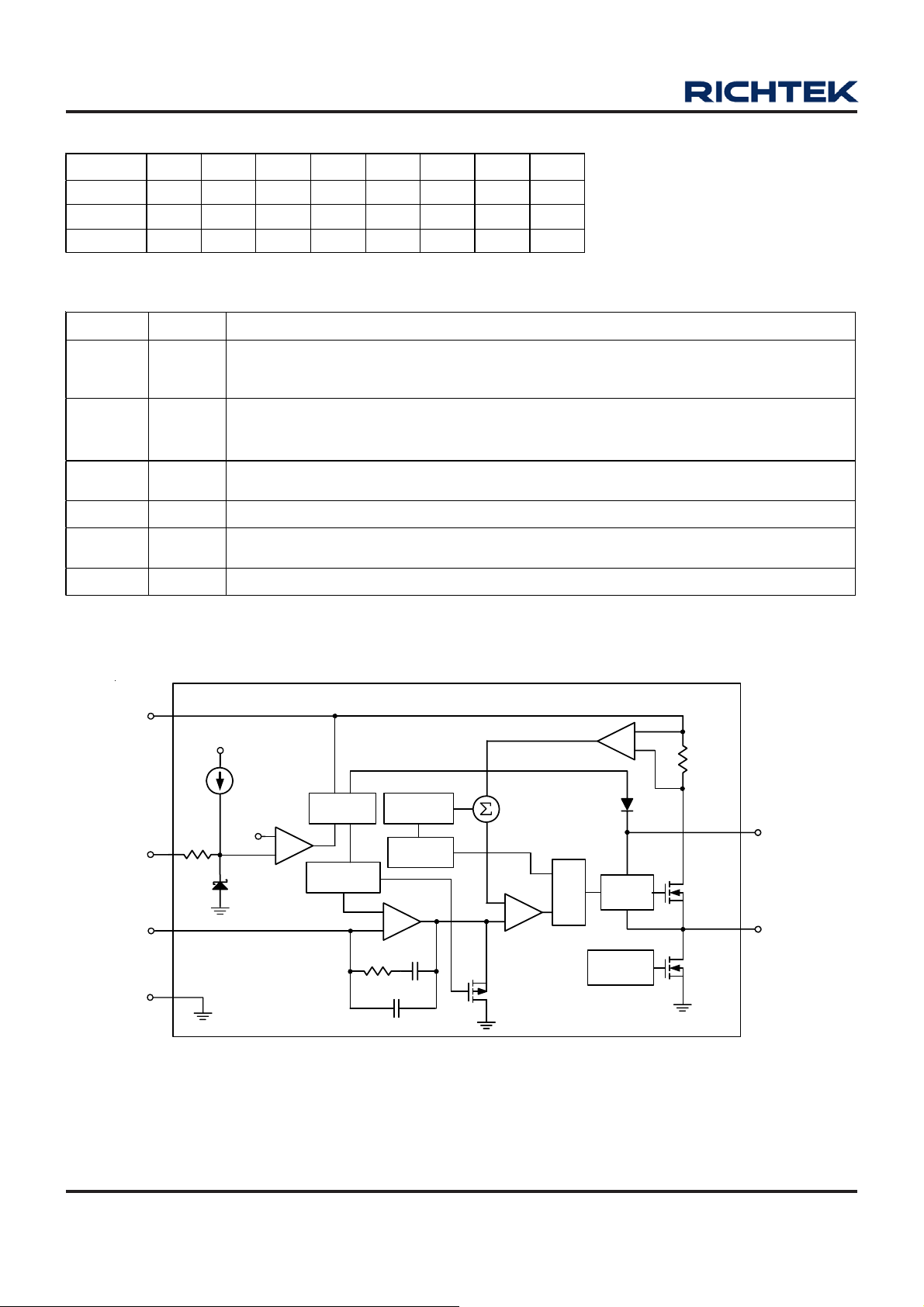
Function Block Diagram
VIN
1µA
+
Shutdown
Comparator
EN
FB
GND
10k
1.1V
3V
Regulator
Reference
400k
Ramp
Generator
Oscillator
1.4MHz
+
EA
30pF
1pF
Current Sense Amp
S
+
PWM
Comparator
OC Limit Clamp
Q
R
X20
Driver
Bootstrap
Control
+
25mΩ
Ω
BOOT
PHASE
DS8259-03 March 2011www.richtek.com
2
Absolute Maximum Ratings (Note 1)
RT8259
z Supply V oltage, V
z PHASE V oltage ----------------------------------------------------------------------------------------------------- −0.3V to (V
z BOOT V oltage ------------------------------------------------------------------------------------------------------- V
z All Other Pins-------------------------------------------------------------------------------------------------------- 0.3V to 6V
z Output V oltage ------------------------------------------------------------------------------------------------------ −0.3V to 15V
z Power Dissipation, P
------------------------------------------------------------------------------------------------ 26V
IN
@ T
D
= 25°C
A
PHASE
+ 6V
+ 0.3V)
IN
T/SOT-23-6 ----------------------------------------------------------------------------------------------------------- 0.4W
z Package Thermal Resistance (Note 2)
T/SOT-23-6, θJA------------------------------------------------------------------------------------------------------ 250°C/W
z Junction T emperature ---------------------------------------------------------------------------------------------- 150°C
z Lead T emperature (Soldering, 10 sec.) ------------------------------------------------------------------------ 260°C
z Storage T emperature Range -------------------------------------------------------------------------------------- −65°C to 150 °C
z ESD Susceptibility (Note 3)
HBM (Human Body Mode)---------------------------------------------------------------------------------------- 2kV
MM (Machine Mode) ----------------------------------------------------------------------------------------------- 200V
Recommended Operating Conditions (Note 4)
z Supply V oltage, V
z Output V oltage, V
z EN Voltage, V
z Junction T emperature Range ------------------------------------------------------------------------------------- −40°C to 125°C
z Ambient T emperature Range ------------------------------------------------------------------------------------- −40°C to 85°C
------------------------------------------------------------------------------------------------ 4.5V to 24V
IN
---------------------------------------------------------------------------------------------- 0.8V to 15V
OUT
----------------------------------------------------------------------------------------------------- 0V to 5.5V
EN
Electrical Characteristics
(VIN = 12V, TA = 25° C unless otherwise specified)
Parameter Symbol Test Conditions Min Typ Max Unit
Feedback Reference Voltage VFB 4.5V ≤ V
Feedback Current IFB VFB = 0.8V -- 0.1 0.3 μA
Switch On Resistance R
Switch Lea kage V
Cur rent Limit I
LIM
-- 0.3 -- Ω
DS(ON)
EN
V
BOOT
Oscillator Frequency fSW 1.2 1.4 1.6 MHz
Maximum Duty Cycle -- 80 -- %
Minimum On-Time tON -- 100 -- ns
Under Voltage Lockout
Threshold
Under Voltage Lockout
Threshold Hysteresis
EN Input Voltage
Logic-High VIH 1.4 -- -Logic-Low V
EN Pull Up Current V
Rising 3.9 4.2 4.5 V
-- 200 -- mV
-- -- 0.4
IL
EN
≤ 24V 0.784 0.8 0.816 V
IN
= 0V, V
− V
PHASE
= 0V -- -- 10 μA
PHASE
= 4.8V 1.6 2.1 -- A
V
= 0V -- 1 -- μA
T o be continued
DS8259-03 March 2011 www.richtek.com
3

RT8259
Parameter Symbol Test Conditions Min Typ Max Unit
Shutdown Current I
Quiescent Current IQ V
SHDN
V
EN
EN
= 0V -- 25 -- μA
= 2V, VFB = 1V (Not Switching) -- 0.55 1 mA
Therma l Shutdown TSD -- 150 -- °C
Note 1. Stresses listed as the above "Absolute Maximum Ratings" may cause permanent damage to the device. These are for
stress ratings. Functional operation of the device at these or any other conditions beyond those indicated in the
operational sections of the specifications is not implied. Exposure to absolute maximum rating conditions for extended
periods may remain possibility to affect device reliability.
Note 2. θ
Note 3. Devices are ESD sensitive. Handling precaution is recommended.
Note 4. The device is not guaranteed to function outside its operating conditions.
is measured in the natural convection at TA = 25°C on a high effective four layers thermal conductivity test board of
JA
JEDEC 51-7 thermal measurement standard.
DS8259-03 March 2011www.richtek.com
4
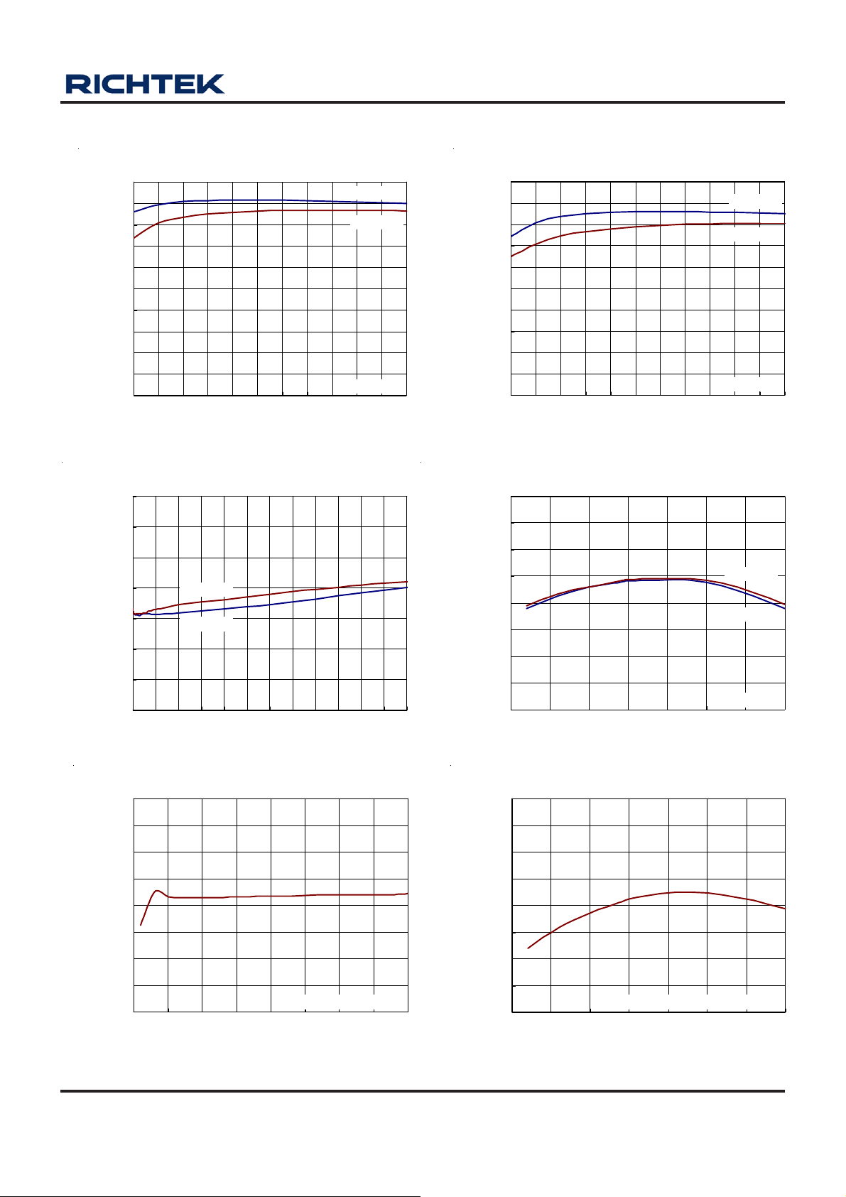
Typical Operating Characteristics
RT8259
Efficiency vs. Load Current
100
90
80
70
60
50
40
Efficiency (%)
30
20
10
0
0.1 0.2 0.3 0.4 0.5 0.6 0.7 0.8 0.9 1 1.1 1.2
Load C ur rent (A)
Output Voltage vs. Load Current
3.333
3.328
3.323
Output Vol t ag e (V)
3.318
3.313
3.308
3.303
3.298
0 0.1 0.2 0.3 0.4 0.5 0.6 0.7 0.8 0.9 1 1.1 1.2
VIN = 24V
VIN = 12V
Load C ur ren t ( A)
VIN = 12V
VIN = 24V
V
= 5V
OUT
Efficiency vs. Load Current
100
90
80
70
60
50
40
Efficiency (%)
30
20
10
0
0.1 0.2 0.3 0.4 0.5 0.6 0.7 0.8 0.9 1 1.1 1.2
Load Current (A)
Output Voltage vs. Temperature
3.38
3.36
3.34
3.32
3.30
3.28
Output Vol tage ( V)
3.26
3.24
3.22
-50 -25 0 25 50 75 100 125
Temper at ur e (°C)
VIN = 12V
VIN = 24V
V
= 3.3V
OUT
VIN = 24V
VIN = 12V
I
OUT
= 0A
Frequency vs. Input Voltage
1.55
1.50
1.45
1.40
1.35
1.30
Frequency (MHz)
1.25
1.20
V
= 3.3V, I
1.15
4 6.5 9 11.51416.51921.524
Input Vol tage (V)
OUT
OUT
= 0.3A
1.55
1.50
1.45
1.40
1.35
1.30
Frequenc y (MHz) 1
1.25
1.20
1.15
-50 -25 0 25 50 75 100 125
Frequency vs. Temperature
VIN = 12V, V
Temperature (°C)
= 3.3V, I
OUT
OUT
= 0.3A
DS8259-03 March 2011 www.richtek.com
5

RT8259
)
0.9
0.8
0.7
0.6
0.5
0.4
0.3
Quiescent Cur rent (mA)
0.2
0.1
V
OUT
(50mV/Div)
Quiescent Current vs. Input Voltage
VEN = 2V, VFB = 1V
4 6.5 9 11.5 14 16.5 19 21.5 24
Input Volt age ( V)
Load Transient Response
VIN = 12V, V
= 3.3V, I
OUT
= 0.6A to 1.2A
OUT
0.9
0.8
0.7
0.6
0.5
0.4
0.3
Quie scent Current (mA
0.2
0.1
V
OUT
(50mV/Div)
Quiescent Current vs. Temperature
VIN = 24V
VIN = 12V
VEN = 2V, VFB = 1V
-50 -25 0 25 50 75 100 125
Temperature (°C)
Load Transient Response
VIN = 12V, V
OUT
= 3.3V, I
= 0A to 1.2A
OUT
I
OUT
(500mA/Div)
V
OUT
(5mV/Div)
V
PHASE
(10V/Div)
I
L
(1A/Div)
Time (50μs/Div)
Switching
VIN = 12V, V
Time (250ns/Div)
OUT
= 3.3V, I
OUT
= 1.2A
I
OUT
(500mA/Div)
V
OUT
(5mV/Div)
V
PHASE
(10V/Div)
I
L
(1A/Div)
Time (50μs/Div)
Switching
VIN = 20V, V
Time (250ns/Div)
= 3.3V, I
OUT
OUT
= 1.2A
DS8259-03 March 2011www.richtek.com
6

RT8259
V
EN
(5V/Div)
V
OUT
(1V/Div)
I
IN
(500mA/Div)
Power On from EN
VIN = 12V, V
Time (250μs/Div)
OUT
= 3.3V, I
OUT
= 1.2A
V
EN
(5V/Div)
V
OUT
(1V/Div)
I
IN
(500mA/Div)
Power Off from EN
VIN = 12V, V
Time (100μs/Div)
= 3.3V, I
OUT
OUT
= 1.2A
DS8259-03 March 2011 www.richtek.com
7
RT8259
Application Information
The RT8259 is a high voltage buck converter that can support
the input voltage range from 4.5V to 24V and the output
current can be up to 1.2A.
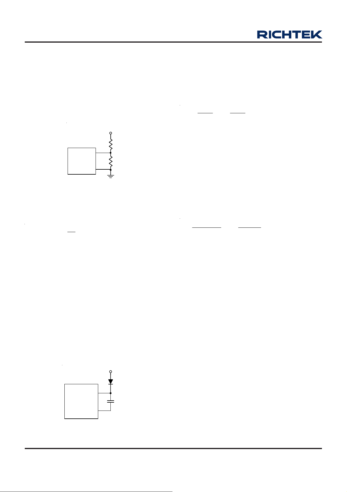
Output Voltage Setting
The resistive voltage divider allows the FB pin to sense a
fraction of the output voltage a s shown in Figure 1.
V
OUT
R1
FB
RT8259
GND
R2
Figure 1. Output V oltage Setting
For adjustable voltage mode, the output voltage is set by
an external resistive voltage divider according to the
following equation :
R1
V = V1
OUT FB
⎛⎞
+
⎜⎟
R2
⎝⎠
Where VFB is the feedback reference voltage (0.8V typ.).
Inductor Selection
The inductor value and operating frequency determine the
ripple current according to a specific input and output
voltage. The ripple current ΔI
increases with higher V
L
and decrea ses with higher inducta nce.
VV
⎡⎤⎡ ⎤
OUT OUT
I = 1
Δ×−
L
⎢⎥⎢ ⎥
fL V
×
⎣⎦⎣ ⎦
IN
Having a lower ripple current reduces not only the ESR
losses in the output ca pacitors but also the output voltage
ripple. High frequency with small ripple current ca n achieve
highest efficiency operation. However , it requires a large
inductor to achieve this goal.
For the ripple current selection, the value of ΔI
= 0.4(I
L
MAX
will be a rea sonable starting point. The largest ri pple current
occurs at the highest VIN. To guarantee that the ripple
current stays below the specified maximum, the inductor
value should be chosen according to the following
equation :
⎡⎤⎡ ⎤
VV
L = 1
OUT OUT
⎢⎥⎢ ⎥
fI V
×Δ
L(MAX) IN(MAX)
⎣⎦⎣ ⎦
×−
Inductor Core Selection
IN
)
External Bootstra p Diode
Connect a 10nF low ESR cera mic ca pa citor between the
BOOT pin and SW pin. This capacitor provides the gate
driver voltage for the high side MOSFET .
It is recommended to add an external bootstrap diode
between an external 5V and the BOOT pin f or ef f iciency
improvement when input voltage is lower tha n 5.5V or duty
ratio is higher than 65%. The bootstra p diode ca n be a low
cost one such as 1N4148 or BAT54.
The external 5V ca n be a 5V fixed input from syste m or a
5V output of the RT8259.
5V
BOOT
RT8259
PHASE
10nF
Figure 2. External Bootstra p Diode
The inductor type must be selected once the value for L is
known. Generally spe aking, high efficiency converters ca n
not afford the core loss found in low cost powdered iron
cores. So, the more expensive ferrite or mollypermalloy
cores will be a better choice.
The selected inductance rather than the core size for a
fixed inductor value is the key for a ctual core loss. As the
inductance increa ses, core losses decre ase. U nfortunately ,
increa se of the inductance requires more turns of wire a nd
therefore the copper losses will increa se.
Ferrite designs are preferred at high switching frequency
due to the characteristics of very low core losses. So,
design goals can focus on the reduction of copper loss
and the saturation prevention.
Ferrite core material saturates “hard”, which means that
inductance colla pses abruptly when the pea k design current
is exceeded. The previous situation results in an abrupt
increa se in inductor ripple current and consequent output
voltage ripple.
Do not allow the core to saturate!
DS8259-03 March 2011www.richtek.com
8

RT8259
Different core materials a nd sha pes will cha nge the size/
current and price/current relationshi p of an inductor .
T oroid or shielded pot cores in ferrite or permalloy materials
are small and do not radiate energy. However, they are
usually more expensive than the similar powdered iron
inductors. The rule for inductor choice mainly depends on
the price vs. size requirement and a ny radiated f ield/EMI
requirements.
Diode Selection
When the power switch turns off, the path for the current
is through the diode connected between the switch output
and ground. This forward biased diode must have a
minimum voltage drop and re covery times. Schottky diode
is recommended and it should be able to handle those
current. The reverse voltage rating of the diode should be
greater than the maximum in put voltage, and current rating
should be greater than the maximum load current. For
more detail, plea se refer to T a ble 4.
CIN and C
The input ca pacita nce, C
Selection
OUT
is needed to filter the tra pezoidal
IN,
current at the source of the top MOSFET . T o prevent large
ripple current, a low ESR input capacitor sized for the
maximum RMS current should be used. The RMS current
is given by :
V
I = I 1
RMS OUT(MAX)
OUT
VV
This formula has a maximum at V
I
= I
RMS
/2. This simple worst-ca se condition is commonly
OUT
V
IN
IN OUT
−
IN
= 2V
OUT
, where
used for design because even significa nt deviations do not
offer much relief.
Choose a capacitor rated at a higher temperature than
required. Several ca pacitors may also be paralleled to meet
size or height requirements in the design.
The selection of C
is determined by the required Effective
OUT
Series Resistance (ESR) to mini mize voltage ripple.
Moreover, the a mount of bulk ca pa citance is also a key f or
C
selection to ensure that the control loop is stable.
OUT
Loop stability can be che cked by viewing the load transient
response a s described in a later se ction.
The output ripple, ΔV
VIESR
Δ≤Δ +
OUT L
⎡⎤
⎢⎥
⎣⎦
, is determined by :
OUT
1
8fC
OUT
The output ripple will be highest at the maximum input
voltage since ΔIL increases with input voltage. Multiple
ca pa citors placed in parallel may be needed to meet the
ESR and RMS current ha ndling requirement. Dry ta ntalum,
special polymer, aluminum electrolytic and ceramic
capacitors are all available in surface mount packages.
Special polymer capacitors offer very low ESR value.
However, it provide s lower capa citance den sity than other
types. Although Tantalum capacitors have the highest
ca pa cita nce den sity, it is i mporta nt to only use types that
pass the surge test for use in switching power supplies.
Aluminum electrolytic ca pacitors have significa ntly higher
ESR. However, it ca n be used in cost-sensitive a pplications
for ripple current rating and long term reliability
considerations. Cera mic capa citors have excellent low ESR
characteristics but ca n have a high voltage coefficient a nd
audible piezoelectric effects. The high Q of ceramic
ca pacitors with tra ce inductance ca n also lead to significant
ringing.
Higher values, lower cost ceramic capacitors are now
becoming available in smaller ca se sizes. Their high ri pple
current, high voltage rating and low ESR ma ke them ideal
for switching regulator a pplications. However, care must
be taken when these capacitors are used at input and
output. When a cera mic ca pacitor is used at the in put and
the power is supplied by a wall ada pter through long wires,
a load step at the output can induce ringing at the input,
VIN. At best, this ringing can couple to the output a nd be
mistaken as loop instability. At worst, a sudden inrush of
current through the long wires can potentially cause a
voltage spike at V
large enough to damage the part.
IN
Checking T ransient Re spon se
The regulator loop response ca n be checked by looking at
the load transient response. Switching regulators take
several cycles to respond to a step in load current. When
a load step occurs, V
equal to ΔI
C
generating a feedback error signal f or the regulator to
OUT
return V
time, V
OUT
(ESR) also begins to charge or discharge
LOAD
to its steady-state value. During this recovery
OUT
can be monitored f or overshoot or ringing that
immediately shifts by a n a mount
OUT
would indicate a stability problem.
DS8259-03 March 2011 www.richtek.com
9
RT8259
Thermal Considerations
For continuous operation, do not exceed the maximum
operation junction temperature 125°C. The maximum power
dissipation depends on the thermal resistance of IC
package, PCB layout, the rate of surroundings airflow a nd
temperature difference between junction to a mbient. The
maximum power dissipation ca n be calculated by following
formula :
P
where T
D(MAX)
= (T
J(MAX)
− TA) / θ
J(MAX)
JA
is the maximum operation junction
temperature, TA is the a mbient temperature and the θJA is
the junction to ambient thermal re sistance.
For recommended operating conditions specification of the
RT8259, the maximum junction temperature of the die is
125°C. The junction to a mbient thermal resista nce θJA is
layout dependent. For T/SOT-23-6 pa ckage, the thermal
resistance θJA is 120°C/W on standard JEDEC 51-7 f ourlayers thermal test board. The maximum power dissipation
at TA = 25°C can be calculated by following f ormula :
P
= (125°C − 25°C) / (250°C/W) = 0.4W for
D(MAX)
T/SOT-23-6 pa ckages
The maximum power dissipation depends on operating
ambient te mperature for fixed T
θ
. For RT8259 package s, the Figure 3 of derating curves
JA
and thermal resista nce
J(MAX)
allows the designer to see the effect of rising ambient
temperature on the maximum power allowed.
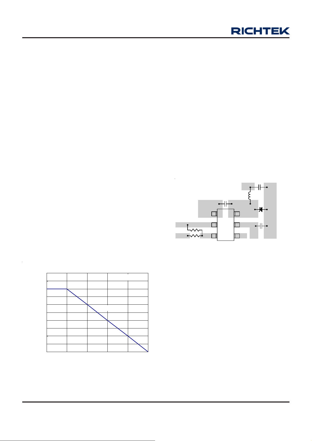
Layout Consideration
Follow the PCB layout guidelines for optimal perf ormance
of RT8259.
` Kee p the tra ces of the main current paths a s short and
wide as possible.
` Put the in put cap acitor a s close a s possible to the device
pins (VIN a nd GND).
` LX node is with high frequency voltage swing a nd should
be kept at small area. Keep sensitive components away
from the LX node to prevent stray capa citive noise pickup.
` Pla ce the feedba ck components to the FB pin as close
as possible.
` Conne ct GND to a ground plane f or noise reduction and
thermal dissipation.
C
OUT
V
OUT
L1
D1
61
PHASE
C
VIN
4
EN
IN
GND
V
OUT
R2
R1
BOOT
GND
FB
C
B
235
Figure 4. PCB Layout Guide
0.50
0.45
0.40
0.35
0.30
0.25
0.20
0.15
0.10
0.05
Maximum Power Dissipation (W)
0.00
0255075100125
Single Layer PCB
T/SOT-23-6
Ambient Te m pera tu re ( °C)
Figure 3. Derating Curves f or RT8259 Pa ckages
10
DS8259-03 March 2011www.richtek.com

RT8259
Table 2. Suggested Inductors for L1
Component Supplier
TDK SLF7045 4.7 30 2 7 x 7 x 4.5
TAIYO YUDEN NR8040 4.7 18 4.7 8 x 8 x 4
GOTERND GTSD53 4.7 45 1.87 5 x 5 x 2.8
GOTERND GSSR2 4.7 18 5.7 10 x 10 x 3.8
Table 3. Suggested Capacitors for CIN and COUT
Component Supplier
MURATA GRM31CR61E106K
TDK C3225X5R1E106K
TAIYO YUDEN TMK316BJ106ML 10 1206
MURATA GRM31CR61C226M
TDK C3225X5R1C226M
TAIYO YUDEN EMK316BJ226ML 22 1206
Table 4. Suggested Diode for D1
Component Supplier
DIODES B230A 30 2 DO-214AC
DIODES B330A 30 3 DO-214AC
PANJIT SK23 30 2 DO-214AC
PANJIT SK33 30 3 DO-214AB
Series Inductance (µH) DCR (mΩ) Current Rating (A) Dimensions (mm)
Part No. Capacitance (µF) Case Size
10 1206
10 1206
22 1206
22 1206
Series V
RRM
(V) I
(A) Package
OUT
DS8259-03 March 2011 www.richtek.com
11
RT8259
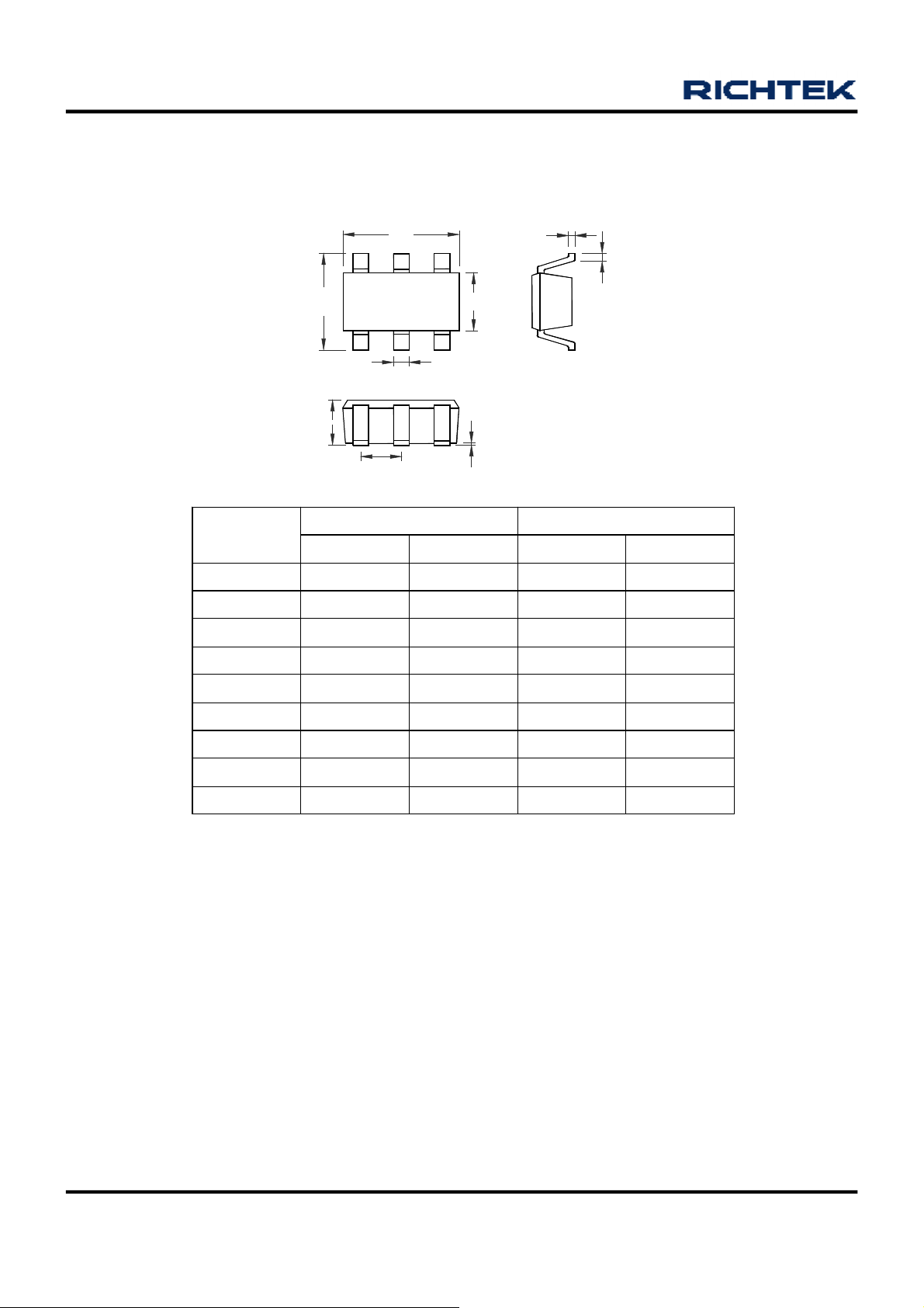
Outline Dimension
H
D
L
C
b
A
e
Dimensions In Millimeters
Symbol
Min Max Min Max
A 0.889 1.295 0.031 0.051
A1 0.000 0.152 0.000 0.006
B 1.397 1.803 0.055 0.071
b 0.250 0.560 0.010 0.022
C 2.591 2.997 0.102 0.118
D 2.692 3.099 0.106 0.122
e 0.838 1.041 0.033 0.041
B
A1
Dimensions In Inches
12
H 0.080 0.254 0.003 0.010
L 0.300 0.610 0.012 0.024
SOT-23-6 Surface Mount Package
DS8259-03 March 2011www.richtek.com
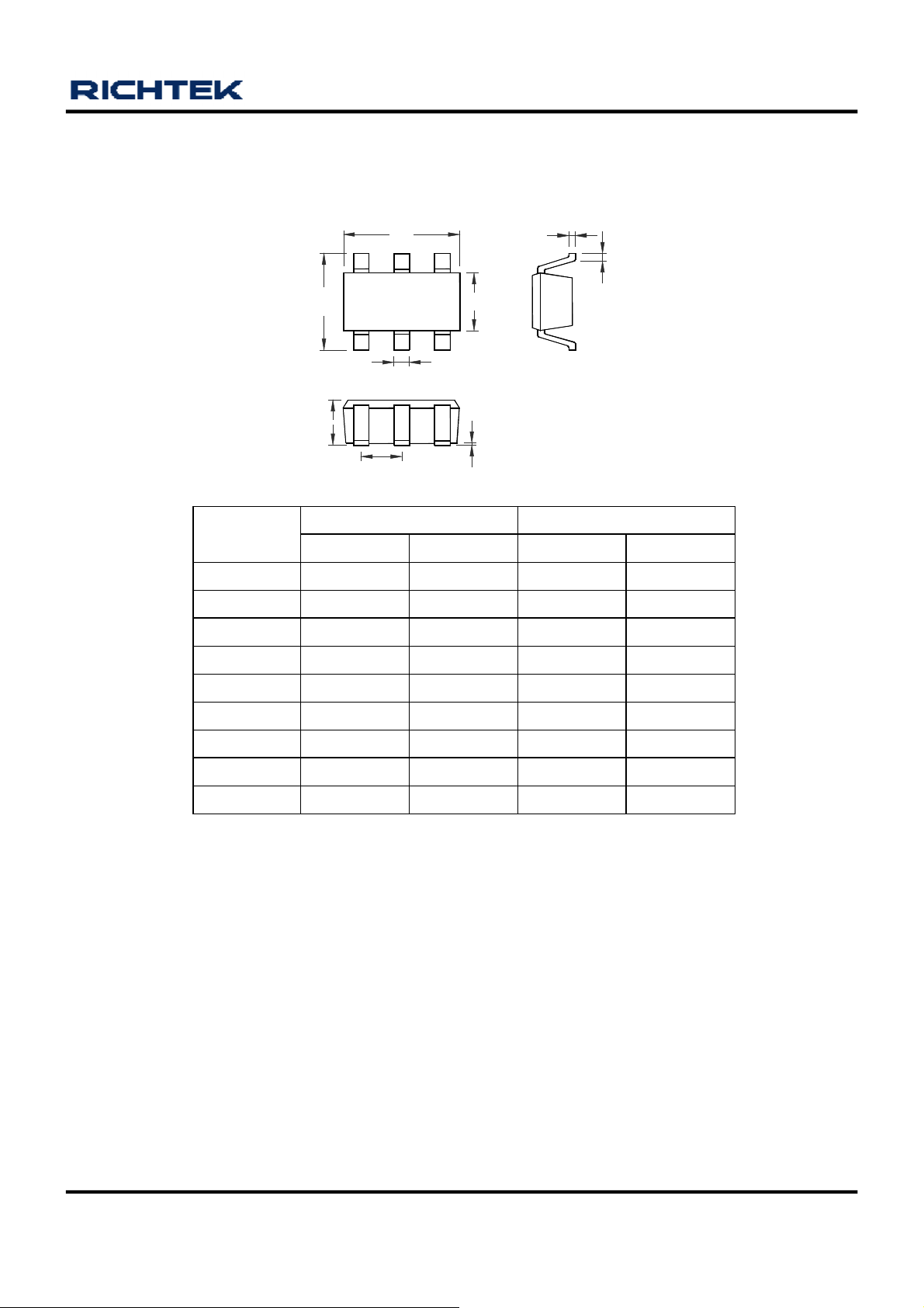
RT8259
H
D
L
C
b
A
e
Dimensions In Millimeters
B
A1
Dimensions In Inches
Symbol
Min Max Min Max
A 0.700 1.000 0.028 0.039
A1 0.000 0.100 0.000 0.004
B 1.397 1.803 0.055 0.071
b 0.300 0.559 0.012 0.022
C 2.591 3.000 0.102 0.118
D 2.692 3.099 0.106 0.122
e 0.838 1.041 0.033 0.041
H 0.080 0.254 0.003 0.010
L 0.300 0.610 0.012 0.024
TSOT-23-6 Surface Mount Package
Richtek Technology Corporation
Headquarter
5F, No. 20, Taiyuen Street, Chupei City
Hsinchu, Taiwan, R.O.C.
Tel: (8863)5526789 Fax: (8863)5526611
Information that is provided by Richtek Technology Corporation is believed to be accurate and reliable. Richtek reserves the right to make any change in circuit design,
specification or other related things if necessary without notice at any time. No third party intellectual property infringement of the applications should be guaranteed
by users when integrating Richtek products into any application. No legal responsibility for any said applications is assumed by Richtek.
DS8259-03 March 2011 www.richtek.com
Richtek Technology Corporation
Taipei Office (Marketing)
5F, No. 95, Minchiuan Road, Hsintien City
Taipei County, Taiwan, R.O.C.
Tel: (8862)86672399 Fax: (8862)86672377
Email: marketing@richtek.com
13

 Loading...