

®
RT8811A
Dual-Phase COT Buck PWM Controller with Dynamic Voltage
Control
General Description
The RT8811A is a dual-phase synchronous Buck PWM
controller which is optimized for high performance graphic
microprocessor and computer applications. The IC
integrates a Constant-On-Time (COT) PWM controller, two
MOSFET drivers with internal bootstrap diodes, as well
as channel current balance and protection functions
including Over-Voltage Protection (OVP), Under-Voltage
Protection (UVP), current limit and thermal shutdown into
the WQFN-24L 4x4 package.
The RT8811A adopts R
Current limit is accomplished through continuous inductor-
current-sense, while R
accurate channel current balance. Using the method of
current sampling utilizes the best advantages of each
technique.
The RT8811A features external reference input and PWM-
VID dynamic output voltage control, in which the feedback
voltage is regulated and tracks external input reference
voltage. Other features include adjustable switching
frequency, dynamic phase number control, internal/external
soft-start, power good indicator, and enable functions.
current sensing technique.
DS(ON)
current sensing is used for
DS(ON)
Features
Dual-Phase PWM Controller
Two Embedded MOSFET Drivers and Embedded
Switching Boot Diode
External Reference Input Control
PWM-VID Dynamic Voltage Control
Dynamic Phase Number Control
Lossless R
Internal Fixed and External Adjustable Soft-Start
Built-In 220mA 5V LDO
Adjustable Current Limit Threshold
Adjustable Switching Frequency
UVP/OVP Protection
Shoot-Through Protection and Short Pulse Free
Technology
Single IC Supply Voltage : 4.5V to 13.2V
Support an Ultra-Low Output Voltage as Standby
Voltage
Thermal Shutdown
Thermal Alert Indicator
Power Good Indicator
RoHS Compliant and Halogen Free
Current Sensing for Current Balance
DS(ON)
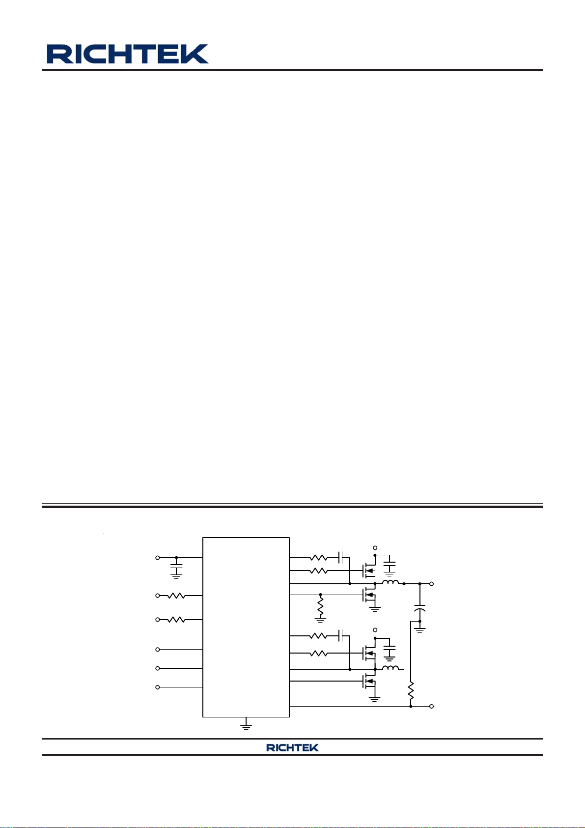
Simplified Application Circuit
V
RT8811A
V
PVCC
PVCC
BOOT1
UGATE1
PHASE1
V
PGOOD
IN
TON
PGOOD
PSI
VID
EN
Copyright 2014 Richtek Technology Corporation. All rights reserved. is a registered trademark of Richtek Technology Corporation.
©
GND
L
G
A
T
E
B
O
O
T
UGATE2
PHASE2
L
G
A
T
E
RGND
1
2
2
DS8811A-02 March 2014 www.richtek.com
IN
V
OUT
V
IN
V
GND_SNS
1
RT8811A
Applications
Motherboard to High End GPU Core Power
High End Desktop PC Memory Core Power
Low Voltage. High Current DC/DC Converter
Voltage Regulator Modules
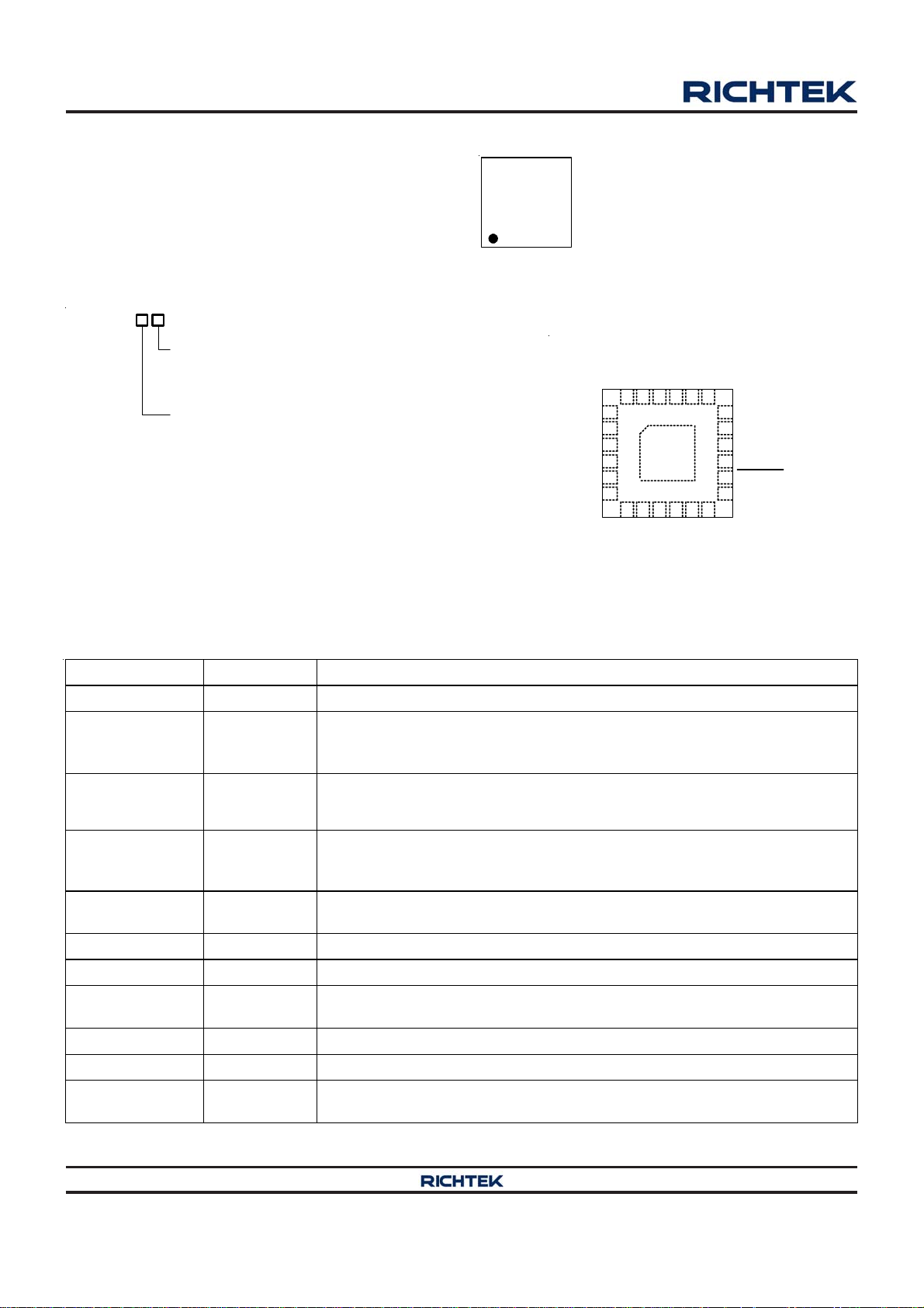
Ordering Information
RT8811A
Package Type
QW : WQFN-24L 4x4 (W-Type)
(Exposed Pad-Option 1)
Lead Plating System
G : Green (Halogen Free and Pb Free)
Note :
Richtek products are :
RoHS compliant and compatible with the current require-
ments of IPC/JEDEC J-STD-020.
Suitable for use in SnPb or Pb-free soldering processes.
Marking Information
0T= : Product Code
0T=YM
YMDNN : Date Code
DNN
Pin Configurations
(TOP VIEW)
LGATE1
GND
VREF
GND
21 20 1924 2223
TON
PVCC
25
RGND
BOOT1
UGATE1
EN
PSI
VID
REFADJ
PHASE1
1
2
3
4
5
6
78910 1211
REFIN
WQFN-24L 4x4
PHASE2
LGATE2
18
BOOT2
17
UGATE2
16
PGOOD
15
VCC
14
TALERT
13
TSNS
SS
VSNS
Function Pin Description
Pin No. Pin Name Pin Function
1 BOOT1 Bootstrap Supply for PWM 1. This pin powers the high-side MOSFET driver.
High-Side Driver of PWM 1. This pin provides the gate drive for the
2 UGATE1
3 EN
4 PSI
5 VID
6 REFADJ Reference Adjustment Output. Refer to PWM-VID Dynamic Voltage Control.
7 REFIN External Reference Input.
8 VREF
9 TON ON-Time/Switching Frequency Adjustment Input.
10 RGND Negative Remote Sense Input. Connect this pin to the ground of output load.
11 VSNS
converter's high-side MOSFET. Connect this pin to the Gate of high-side
MOSFET.
Enable Control Input. Drive EN higher than 1.6V to turn on the controller,
lower than 0.8V to turn it off. If the EN pin is open, it will be pulled to high by
internal circuit.
Power Saving Interface. When the voltage is pulled below 0.8V, the device
will operate into 1 phase DEM. When the voltage is between 2.4V to 5.5V, the
device will operate into 2 phases force CCM.
Programming Output Voltage Control Input. Refer to PWM-VID Dynamic
Voltage Control.
Reference Voltage Output. This is a high precision voltage reference (2V)
from the VREF pin to the RGND pin.
Positive Remote Sense Input. Connect this pin to the positive terminal of
output load.
Copyright 2014 Richtek Technology Corporation. All rights reserved. is a registered trademark of Richtek Technology Corporation.
©
DS8811A-02 March 2014www.richtek.com
2

Pin No. Pin Name Pin Function
Soft-Start Time Setting. Connect an external capacitor to adjust soft-start
12 SS
13 TSNS Temperature Sensing Input.
time. When the external capacitor is removed, the internal soft-start function
will be chose.
RT8811A
14
15 VCC
16 PGOOD Power Good Indicator Output. Active high open-drain output.
17 UGATE2
18 BOOT2 Bootstrap Supply for PWM 2. This pin powers the high-side MOSFET driver.
19 PHASE2
20 LGATE2
21 PVCC
22,
25 (Exposed Pad)
23 LGATE1
24 PHASE1
TALERT
GND
Thermal Alert. Active low open-drain output.
LDO Regulator Output. Connect a minimum 4.7F ceramic capacitor between
this pin and ground.
High-Side Driver of PWM 2. This pin provides the gate drive for the
converter's high-side MOSFET. Connect this pin to the high-side MOSFET.
Switch Node for PWM2. Connect this pin to the Source of high-side MOSFET
together with the Drain of low-side MOSFET and the inductor.
Low-Side Driver of PWM 2. This pin provides the gate drive for the converter's
low-side MOSFET. Connect this pin to the low-side MOSFET.
Supply Voltage Input. Place a high quality bypass capacitor from this pin to
GND.
Ground. Must be connected to GND on PCB. The Exposed pad should be
soldered to a large PCB and connected to GND for maximum thermal
dissipation.
Low-Side Driver of PWM 1. This pin provides the gate drive for the converter's
low-side MOSFET. Connect this pin to the Gate of low-side MOSFET.
Switch Node for PWM1. Connect this pin to the Source of high-side MOSFET
together with the Drain of low-side MOSFET and the inductor.
Copyright 2014 Richtek Technology Corporation. All rights reserved. is a registered trademark of Richtek Technology Corporation.
DS8811A-02 March 2014 www.richtek.com
©
3
RT8811A
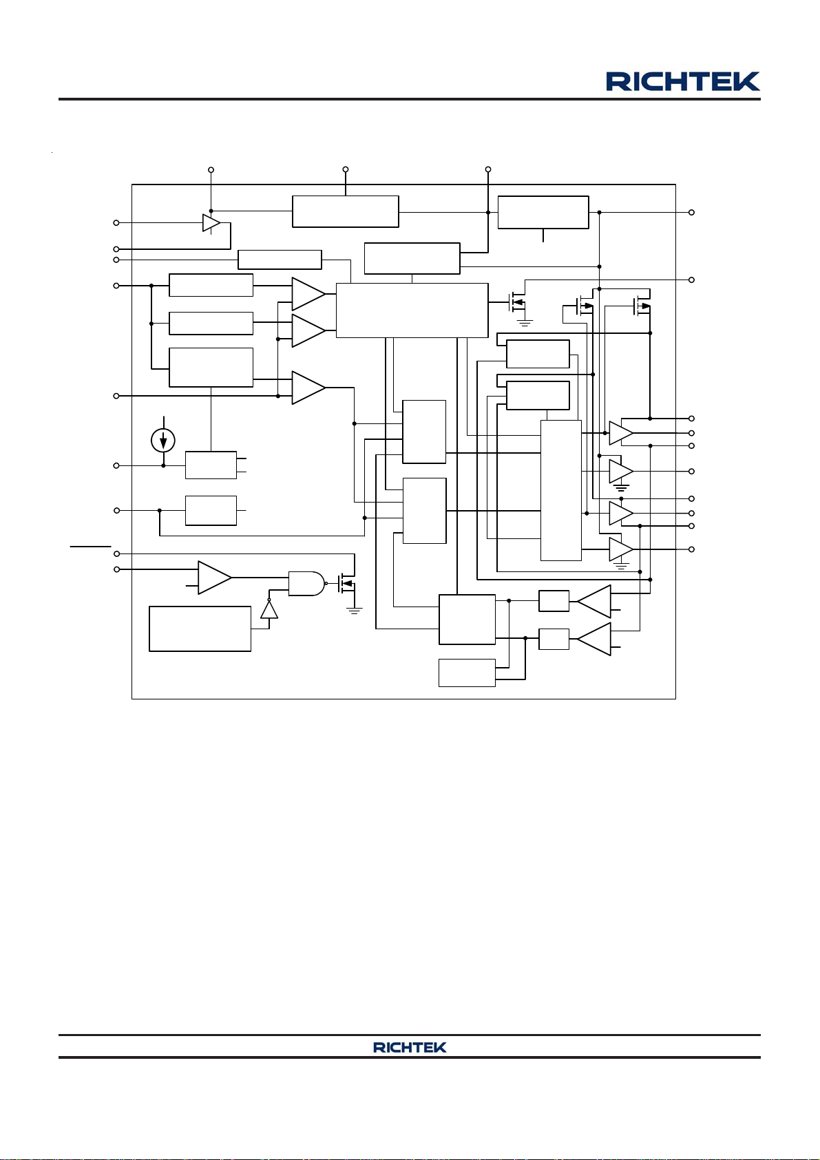
Function Block Diagram
VID
REFADJ
PSI
REFIN
VSNS
EN
TON
TALERT
TSNS
VREF
RGND
OV
150% REFIN
UV
40% REFIN
Soft-Start
& Slew Rate
Control
VA
2µA
Enable
Logic
VIN
Detection
+
1V
-
Internal
Die Temperature
Sense
RGND
Reference Output
Gen. & BG
Mode Select
+
+
-
PWM
CMP
+
-
To Driver Logic
To Power On Reset
To Power On Reset
Power On Reset
& Central Logic
Control & Protection Logic
TON
Gen 1
TON
Gen 2
VCC
Current
Balance
Current
Limit
VCC
Internal
Regulator
VA
Boot-Phase
Detection 1
Boot-Phase
Detection 2
PWM1
Driver
Logic
PWM2
S/H
S/H
PVCC
PGOOD
BOOT1
UGATE1
PHASE1
LGATE1
BOOT2
UGATE2
PHASE2
LGATE2
+
VB
+
VB
-
Copyright 2014 Richtek Technology Corporation. All rights reserved. is a registered trademark of Richtek Technology Corporation.
©
DS8811A-02 March 2014www.richtek.com
4

Operation
RT8811A
The RT8811A integrates a Constant-On-Time (COT) PWM
controller, the controller provides the PWM signal which
relies on the output ripple voltage comparing with internal
reference voltage. Referring to the function block diagram
of TON Genx, the synchronous UGATE driver is turned on
at the beginning of each cycle. After the internal one-shot
timer expires, the UGATE driver will be turned off. The
pulse width of this one-shot is determined by the
converter's input voltage and the output voltage to keep
the frequency fairly constant over the input voltage and
output voltage range. Another one-shot sets a minimum
off-time.
The RT8811A also features a PWM-VID dynamic voltage
control circuit driven by the pulse width modulation
method. This circuit reduces the device pin count and
enables a wide dynamic voltage range.
Current Balance
The RT8811A implements the internal current balance
mechanism in the current loop. The RT8811A senses per
phase current and compares it with the average current. If
the sensed current of any particular phase is higher than
average current, the on-time of this phase will be adjusted
to be shorter.
PGOOD
Current Limit
The current limit circuit employs a unique “valley” current
sensing algorithm. If the magnitude of the current sense
signal at PHASE is above the current limit threshold, the
PWM is not allowed to initiate a new cycle. Thus, the
current to the load exceeds the average output inductor
current, the output voltage falls and eventually crosses
the under-voltage protection threshold, inducing IC
shutdown.
Over-Voltage Protection (OVP)
The output voltage can be continuously monitored for over-
voltage protection. When the output voltage exceeds its
set voltage threshold (If V
> 1.33V, OV = 1.5 x V
REFIN
≤ 1.33V, OV = 2V, or V
REFIN
REFIN
), UGATE goes low and LGATE
is forced high. The controller is latched until VCC is re-
supplied and exceeds the POR rising threshold voltage.
Under-Voltage Protection (UVP)
The output voltage is continuously monitored for under-
voltage protection. When the output voltage is less than
40% of its set voltage, under-voltage protection is triggered
and then both UGATE and LGATE gate drivers are forced
low. The controller is latched until VCC is re-supplied and
exceeds the POR rising threshold voltage.
The power good output is an open-drain architecture.
When the soft-start is finished, the PGOOD open-drain
output will be high impedance.
Soft-Start (SS)
For internal soft-start function, an internal current source
charges an internal capacitor to build the soft-start ramp
voltage. The output voltage will track the internal ramp
voltage during soft-start interval.
For external soft-start function, an additional capacitor
connected from SS to GND will be charged by a current
source and determines the soft-start time.
Copyright 2014 Richtek Technology Corporation. All rights reserved. is a registered trademark of Richtek Technology Corporation.
DS8811A-02 March 2014 www.richtek.com
©
5

RT8811A
Absolute Maximum Ratings (Note 1)
TON to GND ------------------------------------------------------------------------------------------------------- −0.3 to 32V
PVCC to GND ---------------------------------------------------------------------------------------------------- −0.3 to 15V
RGND to GND ---------------------------------------------------------------------------------------------------- −0.7V to 0.7V
PHASEx to GND
DC------------------------------------------------------------------------------------------------------------------- −0.3V to 26V
<20ns -------------------------------------------------------------------------------------------------------------- −8V to 38V
BOOTx to PHASEx --------------------------------------------------------------------------------------------- 15V
UGATEx to GND
DC------------------------------------------------------------------------------------------------------------------- 0.3V to (V
<20ns -------------------------------------------------------------------------------------------------------------- −5V to (V
LGATEx to GND
DC------------------------------------------------------------------------------------------------------------------- −0.3V to (V
<20ns -------------------------------------------------------------------------------------------------------------- −5V to (V
Other Pins--------------------------------------------------------------------------------------------------------- −0.3V to 6V
Power Dissipation, P
@ T
D
= 25°C
A
WQFN-24L 4x4 -------------------------------------------------------------------------------------------------- 3.57W
Package Thermal Resistance (Note 2)
WQFN-24L 4x4, θJA--------------------------------------------------------------------------------------------- 28°C/W
WQFN-24L 4x4, θJC-------------------------------------------------------------------------------------------- 7°C/W
Lead Temperature (Soldering, 10 sec.) --------------------------------------------------------------------- 260°C
Junction Temperature ------------------------------------------------------------------------------------------- 150°C
Storage Temperature Range ---------------------------------------------------------------------------------- −65°C to 150°C
ESD Susceptibility (Note 3)
HBM (Human Body Model)------------------------------------------------------------------------------------ 2kV
BOOT
BOOT
PVCC
PVCC
+ 0.3V)
+ 5V)
+ 0.3V)
+ 5V)
Recommended Operating Conditions (Note 4)
Supply Input Voltage, V
Control Voltage, V
Junction Temperature Range---------------------------------------------------------------------------------- −40°C to 125°C
Ambient Temperature Range---------------------------------------------------------------------------------- −40°C to 85°C
PVCC
-------------------------------------------------------------------------------------- 7V to 20V
IN
----------------------------------------------------------------------------------------- 4.5V to 13.2V
Electrical Characteristics
(T
= 25°C unless otherwise specified)
A
Parameter Symbol Test Conditions Min Typ Max Unit
PWM Controller
PVCC Supply Voltage V
PVCC Supply Current I
PVCC Shutdown Current I
VCC POR Threshold 3.7 4 4.3 V
POR Hysteresis -- 0.3 -- V
VCC (LDO Output) PVCC > 10.8V; I
Copyright 2014 Richtek Technology Corporation. All rights reserved. is a registered trademark of Richtek Technology Corporation.
6
©
4.5 -- 13.2 V
PVCC
SUPPLY
SHDN
EN = 3.3V, Not Switching -- 2 4 mA
EN = 0V, VCC Remains Active -- -- 220 A
< 220mA 4.75 5 5.25 V
VCC
DS8811A-02 March 2014www.richtek.com

RT8811A
Parameter Symbol Test Conditions Min Typ Max Unit
VCC Output Current VCC = 4.5V 220 -- 400 mA
Switching Frequency R
Minimum TON T
Minimum Off-Time T
Zero Current Crossing
Threshold
ON(MIN)
OFF(MIN)
8 -- 8 mV
-- 70 -- ns
-- 300 -- ns
= 500k (Note 5) 270 300 330 kHz
TON
EN Threshold
EN Input Voltage
Logic-High V
Logic-Low V
1.6 -- --
ENH
-- -- 0.8
ENL
V
Mode Decision
PSI High Threshold V
PSI Low Threshold V
Logic-High V
VID Input Voltage
Logic-Low V
Enable Two Phases with FCCM 2.4 -- -- V
PSIH
Enable One Phase with DEM -- -- 0.8 V
PSIL
2 -- --
VIDH
-- -- 1
VIDL
V
Protection Function
Current Limit Setting Current I
Current Limit Setting Current
Temperature Coefficient
9 10 11 A
OCSET
I
OCSET_TC
On the basis of 25C -- 6300 -- ppm/C
Current Limit Threshold 20 -- 20 mV
Current Limit Threshold
Setting Range
Absolute Over-V oltage
Protection Threshold
Relative Over-Voltage
Protection Threshold
OVP Delay
Relative Under-Voltage
Protection Threshold
UVP Delay
Internal Die Temperature
Sense Threshold
50 -- 300 mV
V
OVP, Absolute VREFIN
V
OVP, Relative VREFIN
t
D_OVP
UVP 35 40 45 %
V
UVP
t
D_UVP
-- 5 -- s
-- 3 -- s
-- 95 -- C
1.33V 1.9 2 2.1 V
> 1.33V 145 150 155 %
Thermal Shutdown Threshold TSD -- 140 -- C
TSNS Threshold V
PGOOD Blanking Time
V
Internal Soft-Start Time TSS
OUT
(No Shutting Down) 0.98 1 1.02 V
TSEN
From EN = High to PGOOD = High with
within Regulation Point
V
OUT
From First UGATE to V
Point, V
REFIN
= 1V and V
Regulation
OUT
OUT
Initial = 0V
-- 3.7 -- ms
-- 0.7 -- ms
Soft-Start Current Source ISS -- 5 -- A
Copyright 2014 Richtek Technology Corporation. All rights reserved. is a registered trademark of Richtek Technology Corporation.
DS8811A-02 March 2014 www.richtek.com
©
7

RT8811A
Parameter Symbol Test Conditions Min Typ Max Unit
Er ror Am p l if ier
VSNS Error Comparator
Threshold (Valley)
Reference
V
= 1V 5 -- 5 mV
REFIN
Reference Voltage V
VREF
Sourcing Current = 1mA, VID No
Switching
1.98 2 2.02 V
Driver On-Resistance
UGATE Driver Source R
UGATE Driver Sink R
LGATE Driver Source R
LGATE Driver Sink R
UGATEsr
UGATEsk
LGATEsr
LGATEsk
Dead-Time
I
UGATEx
V
I
LGATEx
V
= 150mA -- 1.5 3
UGATEx
V
PHASEx
= 0.1V -- 2 4
= 150mA -- 1.5 3
= 0. 1V -- 0.7 1.4
LGATEx
From LGATE falling to UGATE rising -- 30 --
ns
From UGATE falling to LGATE rising -- 30 --
Boost Switch Ron R
Note 1. Stresses beyond those listed “Absolute Maximum Ratings” may cause permanent damage to the device. These are
stress ratings only, and functional operation of the device at these or any other conditions beyond those indicated in
the operational sections of the specifications is not implied. Exposure to absolute maximum rating conditions may
affect device reliability.
Note 2. θ
Note 3. Devices are ESD sensitive. Handling precaution is recommended.
Note 4. The device is not guaranteed to function outside its operating conditions.
Note 5. Not production tested. Test condition is V
is measured at T
JA
measured at the exposed pad of the package.
= 25°C on a high effective thermal conductivity four-layer test board per JEDEC 51-7. θJC is
A
PVCC to BOOTx, I
BOOT
= 8V, V
IN
OUT
= 1V, I
= 10mA -- 40 80
BOOT
= 20A using application circuit.
OUT
Copyright 2014 Richtek Technology Corporation. All rights reserved. is a registered trademark of Richtek Technology Corporation.
8
©
DS8811A-02 March 2014www.richtek.com

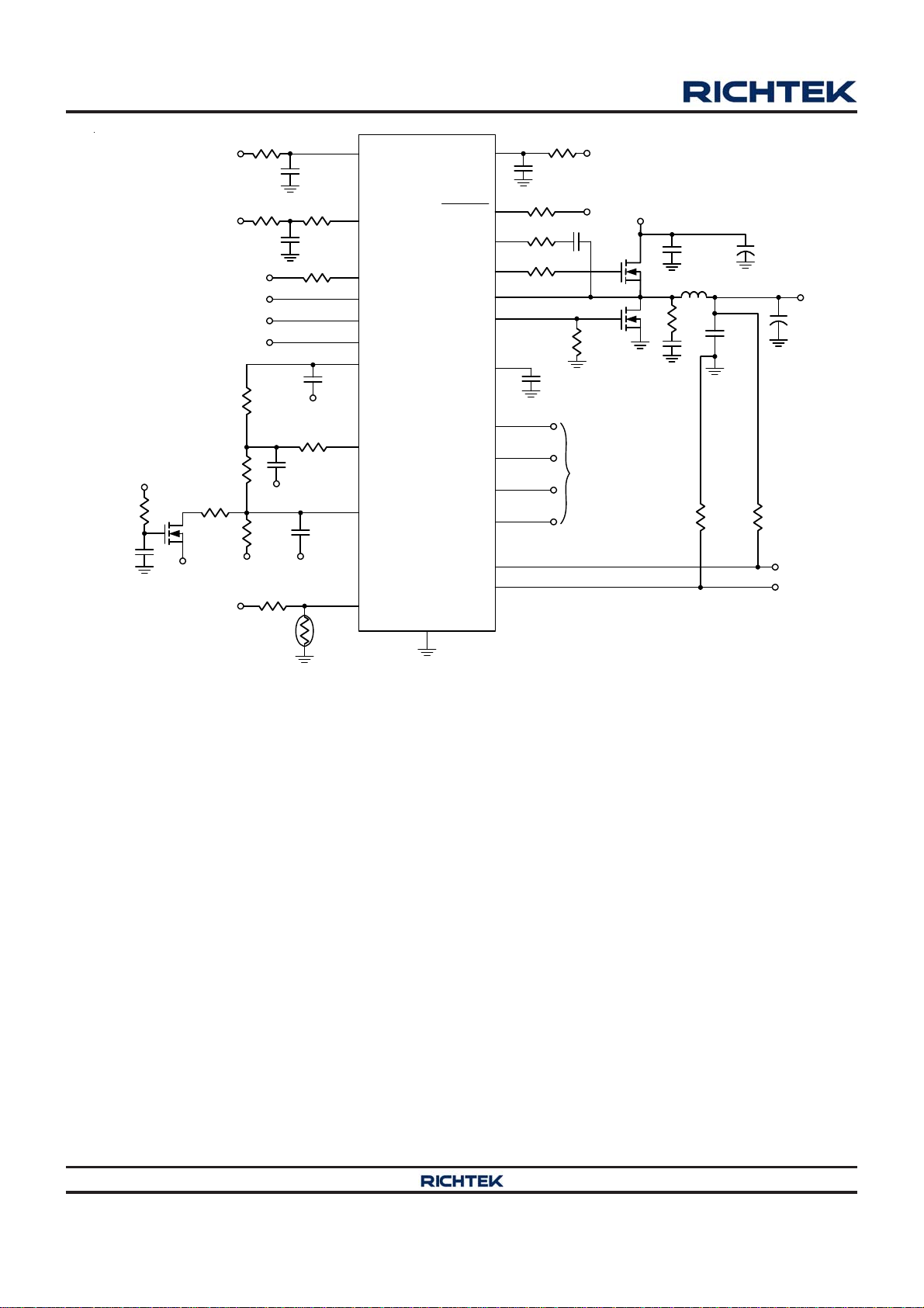
Typical Application Circuit
RT8811A
V_STANDBY
0
NC
RGND
V
PVCC
R
4.75k
R
R
STANDBY
1.07k
Q1
VREF
V
PGOOD
REF1
BOOT
1
2.2
IN
PSI
VID
Enable
0.1µF
RGND
R
C
REFADJ
0
0.01µF
RGND
R
REF2
4.22k
RGND RGND
R
OTSET
10k
2.2µF
R
TON
500k
1µF
100k
REFADJ
6.34k
C
REFIN
NC
R
NTC
10k
21
9
16
4
5
3
8
6
7
13
PVCC
RT8811A
TON
PGOOD
PSI
VID
EN
VREF
REFADJ
REFIN
TSNS
1
VCC
SS
VSNS
RGND
14
1
2
24
23
12
1
17
19
2
11
10
TALERT
BOOT1
UGATE1
PHASE1
LGATE1
BOOT2
UGATE2
PHASE2
LGATE2
GND
22, 25 (Exposed pad)
5
1
4.7µF
30k
0.1µF
0
0
R
10k
C
SS
47pF
0.1µF
0
8
OCSET
V
IN
V
IN
10µF x 6
0.36µH/1.05m
NC
NC
470µF
50V x 2
22µF
x 15
V
OUT
820µF
2.5V x 4
0
0.36µH/1.05m
0
NC
NC
1010
V
OUT_SNS
V
GND_SNS
Figure 1. 2 Active Phase Configuration
Copyright 2014 Richtek Technology Corporation. All rights reserved. is a registered trademark of Richtek Technology Corporation.
DS8811A-02 March 2014 www.richtek.com
©
9
RT8811A
V_STANDBY
0
NC
RGND
V
PVCC
R
R
R
STANDBY
1.07k
Q1
VREF
V
PGOOD
REF1
4.75k
BOOT
1
2.2
IN
PSI
VID
Enable
RGND
R
REFADJ
6.34k
C
REFADJ
0
0.01µF
RGND
R
REF2
4.22k
RGND RGND
R
OTSET
10k
2.2µF
R
TON
500k
1µF
100k
C
NC
R
10k
REFIN
NTC
21
9
16
4
5
3
8
6
7
13
PVCC
RT8811A
TON
PGOOD
PSI
VID
EN
VREF
REFADJ
REFIN
TSNS
1
VCC
SS
BOOT2
VSNS
RGND
14
1
2
24
23
12
1
17
19
2
11
10
TALERT
BOOT1
UGATE1
PHASE1
LGATE1
UGATE2
PHASE2
LGATE2
GND
22, 25 (Exposed pad)
5
1
4.7µF
30k
0
0
C
SS
47pF
0.1µF
R
10k
OCSET
V
IN
0.36µH/1.05m
10µF x 6
NC
NC
22µF
x 15
470µF
50V x 2
V
OUT
820µF
2.5V x 4
8
Floating
0
10 10
V
OUT_SNS
V
GND_SNS
Figure 2. 1 Active Phase Configuration
Copyright 2014 Richtek Technology Corporation. All rights reserved. is a registered trademark of Richtek Technology Corporation.
©
DS8811A-02 March 2014www.richtek.com
10

Typical Operating Characteristics
RT8811A
285.0
282.5
280.0
277.5
(ns)
275.0
ON
T
272.5
Efficiency vs. Load Current
1.0
100
0.9
90
0.8
80
0.7
70
0.6
60
0.5
50
0.4
40
Efficiency (%)
0.3
30
0.2
20
0.1
10
0.0
0
0 102030405060
V
= 0.94V, 2 Phases Operation
OUT
VIN = V
PVCC
= 12V,
Load Current (A)
TON vs. Temperature
Efficiency vs. Load Current
1.0
100
0.9
90
0.8
80
0.7
70
0.6
60
0.5
50
0.4
40
Efficiency (%)
0.3
30
0.2
20
0.1
10
0
0.0
0.01 0.1 1 10
V
= 0.94V, 1 Phase with DEM Operation
OUT
Load Current (A)
V
vs. Temperature
2.04
2.03
2.02
2.01
(V)
2.00
REF
V
1.99
REF
VIN = V
PVCC
= 12V,
270.0
267.5
265.0
-50-250 255075100125
VIN = V
= 12V, No Load
PVCC
Temperature (° C)
Inductor Current vs. Output Current
35
30
25
20
15
10
Inductor Current (A)
5
0
0 102030405060
Phase 1
Phase 2
VIN = V
Output Current (A)
PVCC
= 12V
1.98
1.97
1.96
EN
(5V/Div)
V
OUT
(1V/Div)
UGATE1
(40V/Div)
UGATE2
(40V/Div)
VIN = V
-50-250 255075100125
= 12V, No Load
PVCC
Temperature (° C)
Power On from EN
VIN = V
Time (1ms/Div)
PVCC
= 12V, I
OUT
= 50A
Copyright 2014 Richtek Technology Corporation. All rights reserved. is a registered trademark of Richtek Technology Corporation.
©
DS8811A-02 March 2014 www.richtek.com
11
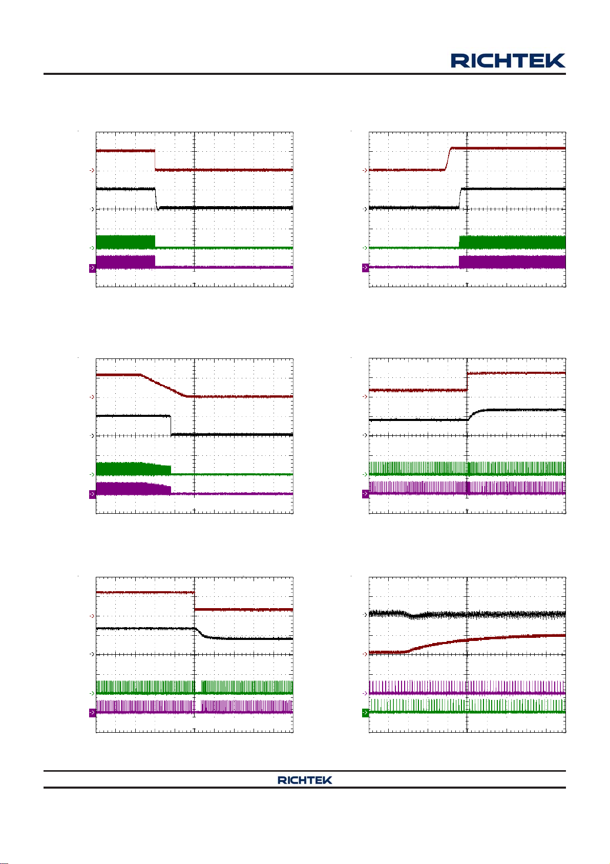
RT8811A
EN
(5V/Div)
V
OUT
(1V/Div)
UGATE1
(40V/Div)
UGATE2
(40V/Div)
PVCC
(10V/Div)
Power Off from EN
VIN = V
Time (1ms/Div)
PVCC
= 12V, I
Power Off from PVCC
OUT
= 50A
PVCC
(10V/Div)
V
OUT
(1V/Div)
UGATE1
(40V/Div)
UGATE2
(40V/Div)
DVID
(2V/Div)
Power On from PVCC
VIN = V
Time (5ms/Div)
PVCC
= 12V, I
OUT
Dynamic Output Voltage Control
VIN = V
PVCC
= 12V
= 50A
V
OUT
(1V/Div)
UGATE1
(40V/Div)
UGATE2
(40V/Div)
DVID
(2V/Div)
V
OUT
(1V/Div)
UGATE1
(40V/Div)
UGATE2
(40V/Div)
VIN = V
PVCC
= 12V, I
OUT
= 50A
Time (5ms/Div)
Dynamic Output Voltage Control
I
OUT
= 50A, V
VIN = V
= 1.22V to 0.7V
REFIN
PVCC
= 12V
V
OUT
(1V/Div)
UGATE1
(40V/Div)
UGATE2
(40V/Div)
V
OUT
(50mV/Div)
I
OUT
(50A/Div)
UGATE1
(40V/Div)
UGATE2
(40V/Div)
I
= 50A, V
OUT
= 0.7V to 1.22V
REFIN
Time (50μs/Div)
Load Transient Response
VIN = V
PVCC
= 12V
Time (50μs/Div)
Copyright 2014 Richtek Technology Corporation. All rights reserved. is a registered trademark of Richtek Technology Corporation.
©
Time (20μs/Div)
DS8811A-02 March 2014www.richtek.com
12
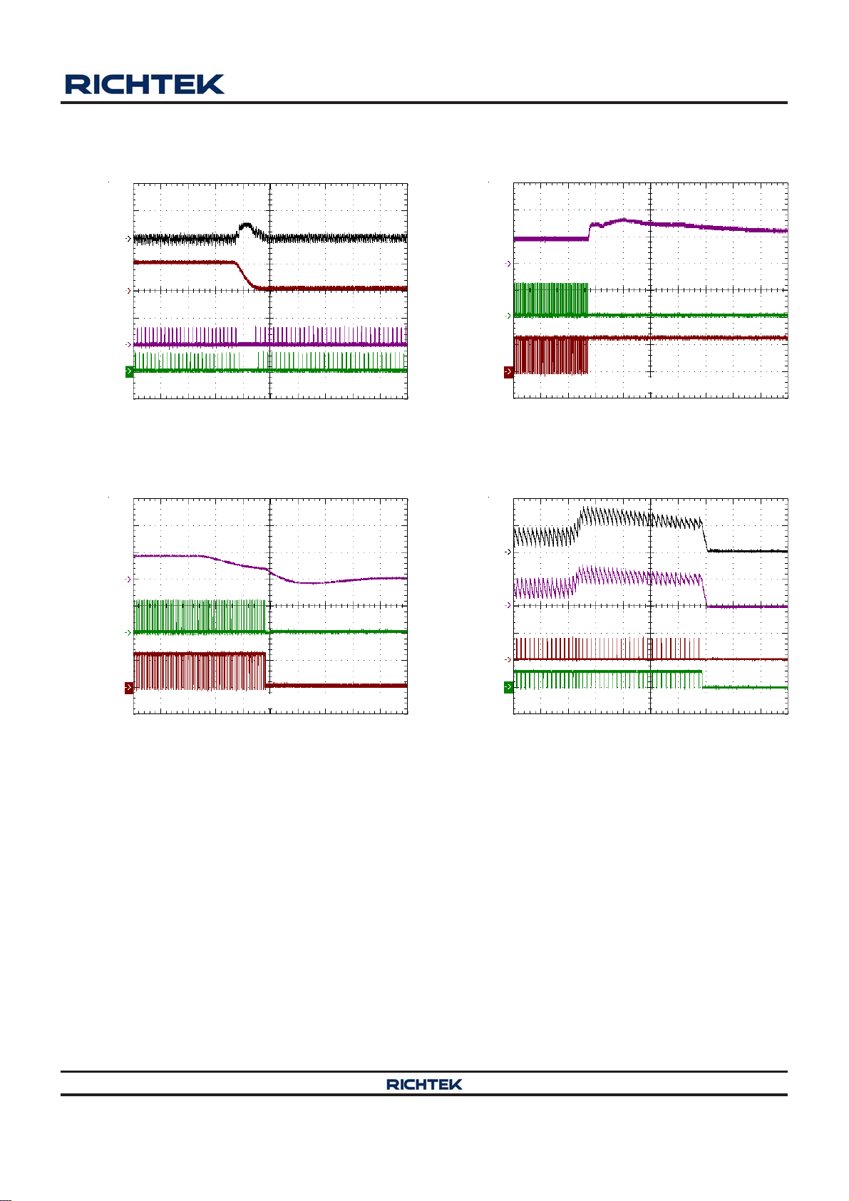
RT8811A
V
OUT
(50mV/Div)
I
OUT
(50A/Div)
UGATE1
(40V/Div)
UGATE2
(40V/Div)
V
VSNS
(1V/Div)
UGATE1
(20V/Div)
LGATE1
(10V/Div)
Load Transient Response
VIN = V
PVCC
Time (20μs/Div)
UVP
VIN = V
PVCC
= 12V, I
OUT
= 12V
= 40A
V
VSNS
(1V/Div)
UGATE1
(20V/Div)
LGATE1
(10V/Div)
I
L2
(10A/Div)
I
L1
(10A/Div)
UGATE1
(30V/Div)
LGATE1
(20V/Div)
OVP
VIN = V
PVCC
Time (100μs/Div)
OCP
VIN = V
= 12V, No Load
= 12V
PVCC
Time (50μs/Div)
Copyright 2014 Richtek Technology Corporation. All rights reserved. is a registered trademark of Richtek Technology Corporation.
©
Time (20μs/Div)
DS8811A-02 March 2014 www.richtek.com
13

RT8811A
Application Information
The RT8811A is a dual-phase synchronous Buck PWM
controller with integrated drivers which is optimized for
high performance graphic microprocessor and computer
applications. A COT (Constant-On-Time) PWM controller
and two MOSFET drivers with internal bootstrap diodes
are integrated so that the external circuit can be easily
designed and the number of component is reduced.
The topology solves the poor load transient response timing
problems of fixed frequency current mode PWM and avoids
the problems caused by widely varying switching
frequencies in conventional constant on-time and constant
off-time PWM schemes.
The RT8811A supports dynamic mode transition function
with various operating states, which include dual-phase
with CCM operation, single phase with diode emulation
mode. These different operating states make the system
efficiency as high as possible.
The RT8811A provides a PWM-VID dynamic control
operation in which the feedback voltage is regulated and
tracks external input reference voltage. It also features
complete fault protection functions including over-voltage,
under-voltage and current limit.
PWM Operation
The RT8811A integrates a Constant-On-Time (COT) PWM
controller, and the controller provides the PWM signal
which relies on the output ripple voltage comparing with
internal reference voltage as shown in Figure 3. Referring
to the function block diagram of TON Genx, the
synchronous UGATE driver is turned on at the beginning
of each cycle. After the internal one-shot timer expires,
the UGATE driver will be turned off. The pulse width of
this one-shot is determined by the converter's input voltage
and the output voltage to keep the frequency fairly constant
over the input voltage and output voltage range. Another
one-shot sets a minimum off-time.
V
OUT
V
PEAK
V
OUT
V
VALLEY
V
REF
0
t
ON
t
Figure 3. Constant On-Time PWM Control
Remote Sense
The RT8811A uses the remote sense path (VSNS and
RGND) to overcome voltage drops in the power lines by
sensing the voltage directly at the end of GPU to make
sure the voltage drops on PCB has no impact on the load
transient response. Normally, to protect remote sense path
disconnecting, there are two resistors (R
) connecting
Local
between local sense path and remote sense path. That
is, in application with remote sense, the R
Local
is
recommended to be 10Ω to 100Ω. If no need of remote
sense, the R
BOOT
UGATE
PHASE
LGATE
RGND
VSNS
is recommended to be 0Ω.
Local
V
IN
R
Local Sense Path
V
OUT
R
Local
Local
GPU
GPU
Remote Sense Path
Figure 4. Output Voltage Sensing
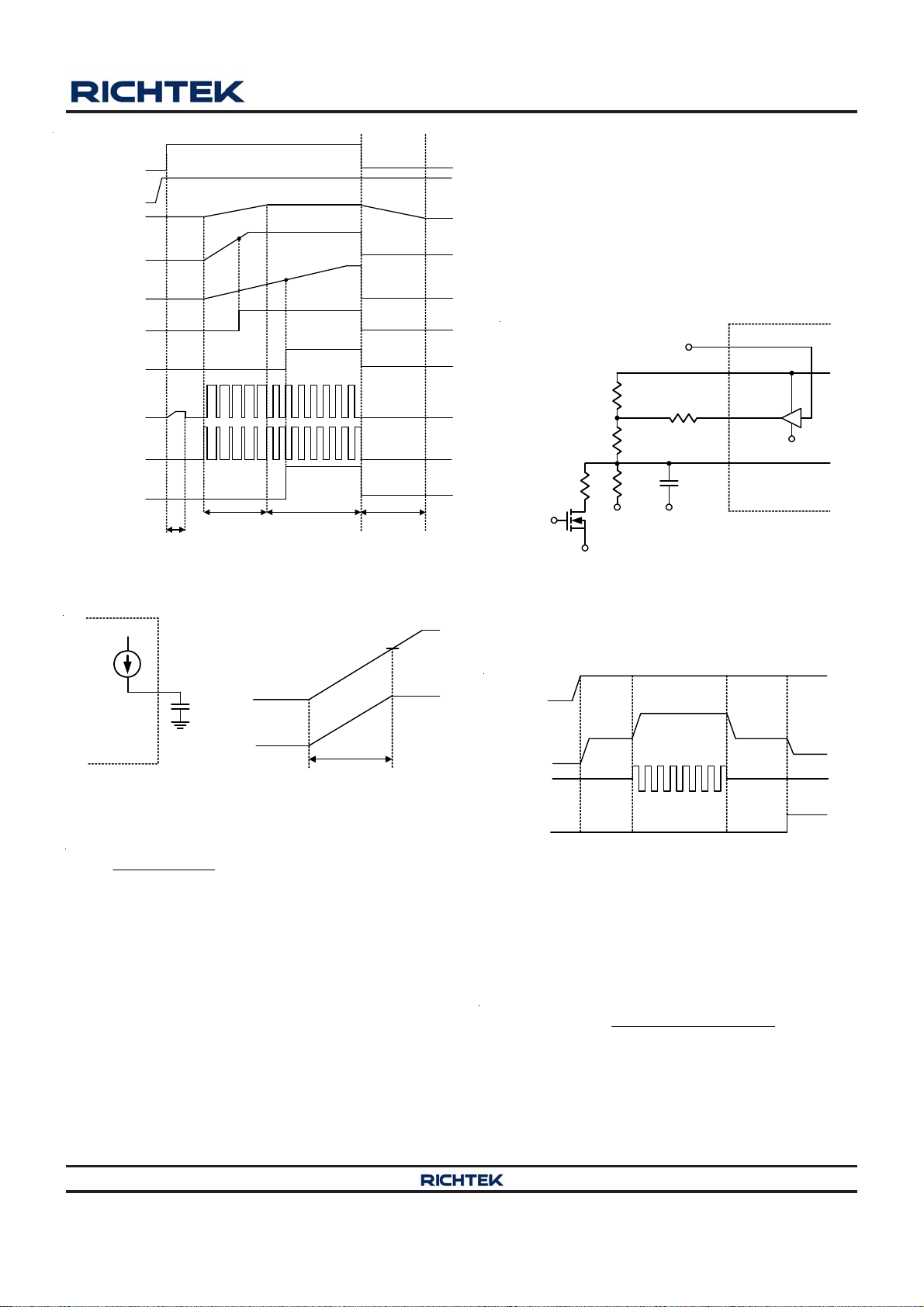
On-Time Control
The on-time one-shot comparator has two inputs. One
input monitors the output voltage, the other input samples
the input voltage and converts it to a current. This input
voltage proportional current is used to charge an internal
on-time capacitor. The on-time is the time required for
the voltage on this capacitor to charge from zero volts to
V
, thereby making the on-time of the high-side switch
OUT
directly proportional to output voltage and inversely
proportional to input voltage. The implementation results
in a nearly constant switching frequency without the need
for a clock generator.
Copyright 2014 Richtek Technology Corporation. All rights reserved. is a registered trademark of Richtek Technology Corporation.
14
©
DS8811A-02 March 2014www.richtek.com

RT8811A
)
2 V 3.2p
T = R
ON TON
OUT
V0.5
IN
and then the switching frequency FS is :
F= V V T
SOUT INON
R
TON
The value of R
/
is the resistor connected from the VIN to TON pin.
can be selected according to Figure 5.
TON
The recommended operation frequency range is 150kHz
to 600kHz.
Frequency vs. R
900
800
700
600
500
400
Frequency (kHz
300
200
150 250 350 450 550 650 750
(kΩ)
R
(kohm)
TON
Figure 5. Frequency vs. R
TON
TON
Active Phase Circuit Setting
The RT8811A can operate in 2/1 phase. For one phase
operation, leave the UGATE2, BOOT2, PHASE2, and
LGATE 2 as floating, and keep the voltage on the PSI pin
under 2.4V before POR.
Diode-Emulation Mode
In diode-emulation mode, the RT8811A automatically
reduces switching frequency at light-load conditions to
maintain high efficiency. As the output current decreases
from heavy-load condition, the inductor current is also
reduced, and eventually comes to the point that its valley
touches zero current, which is the boundary between
continuous conduction and discontinuous conduction
modes. By emulating the behavior of diodes, the low-side
MOSFET allows only partial of negative current when the
inductor freewheeling current reaches negative level. As
the load current is further decreased, it takes longer and
longer to discharge the output capacitor to the level that
requires the next “ON” cycle. In reverse, when the output
current increases from light load to heavy load, the
switching frequency increases to the preset value as the
inductor current reaches the continuous condition.
The switching waveforms may appear noisy and
asynchronous when light loading causes diode-emulation
operation, but this is a normal operating condition that
results in high light load efficiency. Trade-off in DEM noise
vs. light load efficiency is made by varying the inductor
value. Generally, low inductor values produce a broader
efficiency vs. load curve, while higher values result in higher
full-load efficiency (assuming that the coil resistance
remains fixed) and less output voltage ripple. The
disadvantages for using higher inductor values include
larger physical size and degrade load-transient response
(especially at low input voltage levels).
Mode Selection
The RT8811A can operate in 2 phases with force CCM
and 1 phase with DEM according to PSI voltage setting. If
PSI voltage is pulled below 0.8V, the controller will operate
into 1 phase with DEM. In DEM operation, the RT8811A
automatically reduces the operation frequency at light load
conditions for saving power loss. If PSI voltage is pulled
between 2.4V to 5.5V, the controller will switch operation
into 2 phases with force CCM. Moreover, the PSI pin is
Forced-CCM Mode
The low noise, forced-CCM mode disables the zero-
crossing comparator, which controls the low-side switch
on-time. This causes the low-side gate drive waveform to
become the complement of the high-side gate drive
waveform. This in turn causes the inductor current to
reverse at light loads as the PWM loop to maintain a duty
ratio V
/ VIN. The benefit of forced-CCM mode is to
OUT
keep the switching frequency fairly constant.
valid after POR of VR.
Copyright 2014 Richtek Technology Corporation. All rights reserved. is a registered trademark of Richtek Technology Corporation.
DS8811A-02 March 2014 www.richtek.com
©
15

RT8811A
Enable and Disable
The EN pin allows power sequencing between the
controller bias voltage and another voltage rail. The RT8811A
remains in shutdown if the EN pin is lower than 0.8V.
When the EN pin rises above 1.6V, the RT8811A will begin
a new initialization and soft-start cycle. If the EN pin is
open it will be pulled to high by internal circuit.
EN
PVCC
V
OUT
Internal SS
External SS
4V
2V
Power On Reset (POR), UVLO
Power On Reset (POR) occurs when VCC rises above to
approximately 4V (typ.), the RT8811A will reset the fault
latch and preparing the PWM for operation. Below 3.7V
(typ.), the VCC Under-Voltage Lockout (UVLO) circuitry
inhibits switching by keeping UGATE and LGATE low.
Soft-Start
The RT8811A provides an internal soft-start function and
an external soft-start function. The soft-start function is
used to prevent large inrush current and output voltage
overshoot while the converter is being powered up. The
soft-start function automatically begins once the chip is
enabled.
If external capacitor from SS to GND is removed, the
internal soft-start function will be chosen. An internal
current source charges the internal soft-start capacitor
such that the internal soft-start voltage ramps up uniformly.
The output voltage will track the internal soft-start voltage
during the soft-start interval. After the internal soft-start
voltage exceeds the REFIN voltage, the output voltage no
longer tracks the internal soft-start voltage but follows the
REFIN voltage. Therefore, the duty cycle of the UGATE
signal as well as the input current at power up are limited.
The soft-start process is finished until both the single
internal SSOK and external SSOK go high and protection
is not triggered. Figure 6 shows the internal soft-start
sequence.
Internal SSOK
External SSOK
LGATE
UGATE
PGOOD
Soft
Discharged
Current Limit
Programming
Soft-Start
Normal
Figure 6. Internal Soft-Start Sequence
The RT8811A also provides a proximate external soft-start
function, and the external soft-start sequence is shown in
Figure 7, an additional capacitor can be connected from
SS to GND. The external capacitor will be charged by
5μA current source to build soft-start voltage ramp. If
external soft-start function is chosen, the external soft-
start time should be set longer than internal soft-start time
to avoid output voltage tracking the internal soft-start ramp,
the external soft-start time setting is shown in Figure 8,
the recommend external soft-start slew rate is 0.1V/ms
to 0.4V/ms.
Copyright 2014 Richtek Technology Corporation. All rights reserved. is a registered trademark of Richtek Technology Corporation.
16
©
DS8811A-02 March 2014www.richtek.com
RT8811A
PWM VID and Dynamic Output Voltage Control
EN
PVCC
V
OUT
Internal SS
External SS
Internal SSOK
External SSOK
LGATE
UGATE
PGOOD
Current Limit
Programming
4V
Soft-Start
2V
Normal
Soft
Discharged
Figure 7. External Soft-Start Sequence
VCC
V
I
SS
SS
SS
C
SS
V
OUT
t
SS
REFIN
Figure 8. External Soft-Start Time Setting
The soft-start time can be calculated as :
(C V )
t =
SS
where ISS = 5μA (typ.), V
SS REFIN
I
SS
is the voltage of REFIN pin,
REFIN
and CSS is the external capacitor placed from SS to GND.
Power Good Output (PGOOD)
The power good output is an open-drain architecture, and
it requires a pull-up resistor. During soft-start, PGOOD is
actively held low and is allowed to be pulled high after
V
achieved over UVP threshold, under OVP threshold,
OUT
and soft start is completed. In addition if any protection is
triggered during operation, PGOOD will be pulled low
immediately.
The RT8811A features a PWM VID control as shown in
Figure 9, which reduces the number of device pin and
enables a wide dynamic voltage range. The output voltage
is determined by the applied voltage on the REFIN pin.
After VCC POR, the buffer output is available, the VID
PWM duty cycle determines the variable output voltage
at REFIN.
R
STANDBY
Standby
Control
Q1
RGND
R
R
R
RGND
PWM IN
REF1
R
BOOT
REF2
RGND
REFADJ
C
REFIN
VID
VREF
REFADJ
REFIN
Buffer
RGND
Figure 9. PWM VID Analog Circuit Diagram
According to the PWM VID and external circuit control,
the controller can be set three modes which is shown in
Figure 10.
VREF
REFIN
PWM VID
STANDBY
CONTROL
BOOT
MODE
NORMAL
MODE
BOOT
MODE
STANDBY
MODE
Figure 10. PWM VID Time Diagram
Boot Mode
When VID is not driven, and the buffer output is tri-state.
At this time, turn off the switch Q1 and connect a resistor
divider as shown in Figure 9 that can set the REFIN voltage
into V
V = V
BOOT VREF
where V
Choose R
and R
according to below calculation :
BOOT
RRR
REF1 REF2 BOOT
= 2V (typ.)
VREF
to be approximately 10kΩ, and the R
REF2
can be calculated by the following equations :
BOOT
R
REF2
REF1
Copyright 2014 Richtek Technology Corporation. All rights reserved. is a registered trademark of Richtek Technology Corporation.
©
DS8811A-02 March 2014 www.richtek.com
17

RT8811A
RR =
REF1 BOOT
RVV
R = R
REF1 BOOT
R = R
BOOT REF1
REF2 VREF BOOT
RVV
RVV
REF2 VREF BOOT
REF2 VREF BOOT
V
BOOT
V
BOOT
V
BOOT
Standby mode. An external control can provide a very low
voltage to meet V
going to standby mode, If the VID
OUT
pin is not driven and switch Q1 is enabled, the REFIN pin
can be set for standby voltage according to the calculation
below :
V = V
STANDBY VREF
R// R
By choosing R
R R (R // R )
REF1 BOOT REF2 STANDBY
, R
REF1
REF2 STANDBY
REF2
, and R
BOOT
, the R
STANDBY
can
be calculated by the following equation :
R =
STANDBY
RRR V
REF2 REF1 BOOT STANDBY
RVV RRR
REF2 REF STANDBY REF1 REF2 BOOT
R
REF1
Normal Mode
V = V NV
OUT min STEP
where V
V =
STEP
N
is total available voltage step numbers and N is the
max
number of steps at a specific V
VID period (T
is the resolution of each voltage step :
STEP
(V V )
max min
N
max
. The dynamic voltage
OUT
= Tu x N
vid
) is determined by the unit
max
pulse width (Tu) and the available step number (N
The recommend Tu is 27ns.
V
V
min
N = 1
N = 2
REFIN
N = 1
0
T
N = 2
0.5
u
T
= N
max
x T
u
vid
N = N
max
V
max
VID Duty
1
VID Input
VID Input
Figure 11. PWM VID Analog Output
max
).
If the VID pin is driven and switch Q1 is disabled, the
V
can be adjusted from V
REFIN
the zero percent duty cycle voltage value and V
one hundred percent duty cycle voltage value. V
V
can be set according to below calculation :
max
R
V = V
min VREF
V = V
R R // (R R )
REF1 REFADJ BOOT REF2
max VREF
By choosing R
R // (R R )
REF1
REF2
RR
REFADJ BOOT REF2
REF2 BOOT
(R // R ) R R
REF1 REFADJ BOOT REF2
, R
, and R
REF2
to V
min
max
R
REF2
, the R
BOOT
, where V
max
min
can be
REFADJ
is
min
is the
and
calculated by the following equation :
RV
R =
REFADJ
The relationship between VID duty and V
Figure 11, and V
REF1 min
VV
max min
REFIN
can be set according to the calculation
OUT
is shown in
below :
VID Slew Rate Control
In RT8811A, the V
slew rate is proportional to PWM
REFIN
VID duty. The rising time and falling time are the same
because the voltage of REFIN pin traveling is the same. In
normal mode, the V
by C
When choose C
SR =
R = (R // R ) // (R +R )
SR REF1 REFADJ BOOT REF2
When choose C
SR =
R = R // R R // R
SR REF1 REFADJ BOOT REF2
or C
REFADJ
(V V ) 80%
REFIN_Final REFIN_initial
REFIN
REFADJ
2.2R C
REFIN
(V V ) 80%
REFIN_Final REFIN_initial
2.2R C
The recommend SR is estimated by C
slew rate SR can be estimated
REFIN
as the following equation :
:
SR REFADJ
:
SR REFIN
.
REFADJ
Copyright 2014 Richtek Technology Corporation. All rights reserved. is a registered trademark of Richtek Technology Corporation.
18
©
DS8811A-02 March 2014www.richtek.com

RT8811A
Current Balance
The RT8811A implements internal current balance
mechanism in the current loop. The RT8811A senses per
phase current signal and compares it with the average
current. If the sensed current of any particular phase is
higher than average current, the on-time of this phase will
be adjusted to be shorter.
Current Limit
The RT8811A provides cycle-by-cycle current limit control
by detecting the PHASE voltage drop across the low-side
MOSFET when it is turned on. The current limit circuit
employs a unique “valley” current sensing algorithm. If
the magnitude of the current sense signal at PHASE is
above the current limit threshold, the PWM is not allowed
to initiate a new cycle.
In order to provide both good accuracy and a cost effective
solution, the RT8811A supports temperature compensated
MOSFET R
DS(ON)
sensing.
In an over-current condition, the current to the load exceeds
the average output inductor current. Thus, the output
voltage falls and eventually crosses the under-voltage
protection threshold, inducing IC shutdown.
Current Limit Setting
Current limit threshold can be set by a resistor (R
OCSET
between LGATE1 and GND. Once PVCC exceeds the
POR threshold and chip is enabled, an internal current
source I
R
OCSET
V
OCSET
R
OCSET
R =
OCSET
where I
(valley inductor current) and I
flows through R
OCSET
. The voltage across
OCSET
is stored as the current limit protection threshold
. After that, the current source is switched off.
can be determined using the following equation :
IR 40mV
VALLEY LGDS(ON)
represents the desired inductor limit current
VALLEY
I
OCSET
is current limit setting
OCSET
current which has a temperature coefficient to compensate
the temperature dependency of the R
If R
is not present, there is no current path for I
OCSET
DS(ON)
.
OCSET
to build the current limit threshold. In this situation, the
current limit threshold is internally preset to 300mV (typ.).
Negative Current Limit
The RT8811A supports cycle-by-cycle negative current
limit. The value of negative current limit is set as the
positive current limit. If negative inductor current is rising
to trigger negative current limit, the low-side MOSFET
will be turned off and the current will flow to input side
through the body diode of the high-side MOSFET. At this
time, output voltage tends to rise because this protection
limits current to discharge the output capacitor. In order
to prevent shutdown because of over-voltage protection,
the low-side MOSFET is turned on again 400ns after it is
turned off. If the device hits the negative current limit
threshold again before output voltage is discharged to the
target level, the low-side MOSFET is turned off and process
repeats. It ensures maximum allowable discharge
capability when output voltage continues to rise. On the
other hand, if the output is discharged to the target level
before negative current limit threshold is reached, the low-
side MOSFET is turned off, the high-side MOSFET is
then turned on, and the device resumes normal operation.
Output Over-V oltage Prote ction (OVP)
The output voltage can be continuously monitored for over-
voltage protection. If REFIN voltage is lower than 1.33V,
the output voltage threshold follows to absolute over-voltage
2V. If REFIN voltage is higher than 1.33V, the output voltage
)
threshold follows relative over-voltage 1.5 x V
OVP is triggered, UGATE goes low and LGATE is forced
high. The RT8811A is latched once OVP is triggered and
can only be released by PVCC or EN power on reset. A
5μs delay is used in OVP detection circuit to prevent false
trigger.
Output Under-Voltage Protection (UVP)
The output voltage can be continuously monitored for under-
voltage protection. When the output voltage is less than
40% of its set voltage, under-voltage protection is triggered
and then all UGATE and LGATE gate drivers are forced
low. There is a 3μs delay built into the UVP circuit to
prevent false transitions. During soft-start, the UVP blanking
time is equal to PGOOD blanking time.
REFIN
. When
Copyright 2014 Richtek Technology Corporation. All rights reserved. is a registered trademark of Richtek Technology Corporation.
DS8811A-02 March 2014 www.richtek.com
©
19

RT8811A
Thermal Monitoring and Temperature Reporting
The RT8811A provides thermal monitoring function via
sensing the TSNS pin voltage, and which can indicate
ambient temperature through the voltage divider R
and R
shown in Figure 12. The voltage of V
NTC
OTSET
TSNS
is
typically set to be higher than 1V, when ambient
temperature rises, V
will fall, the TALERT signal will
TSNS
be pulled to low level if TSNS voltage drops below 1V or
internal die temperature high than 95°C (typ.).
V
TSNS
V
X
R
OTSET
TSNS
R
NTC
Die Temperature
1V
Internal
Sense
+
CMP
-
V
H
TALERT
Figure 12. External OTP Setting
R
where R
can be determined using the following equation :
OTSET
R = R V1
OTSET NTC,T C X
is the thermistor's resistance at OTP trigger
NTC,T°C
temperature.
The standard formula for the resistance of the NTC
thermistor as a function of temperature is given by :
11
β
R=Re
where R
NTC,T C 25 C
is the thermistor's nominal resistance at room
25°C
T 273 298
temperature 25°C, β (beta) is the thermistor's material
constant in Kelvins, and T is the thermistor's actual
temperature in Celsius.
MOSFET Gate Driver
The RT8811A integrates high current gate drivers for the
MOSFETs to obtain high efficiency power conversion in
synchronous Buck topology. A dead-time is used to prevent
the crossover conduction for high-side and low-side
MOSFETs. Because both the two gate signals are off
during the dead-time, the inductor current freewheels
through the body diode of the low-side MOSFET. The
freewheeling current and the forward voltage of the body
diode contribute to the power loss. The RT8811A employs
adaptive dead-time control scheme to ensure safe operation
without sacrificing efficiency. Furthermore, elaborate logic
circuit is implemented to prevent cross conduction. For
high output current applications, two power MOSFETs are
usually paralleled to reduce R
. The gate driver needs
DS(ON)
to provide more current to switch on/off these paralleled
MOSFETs. Gate driver with lower source/sink current
capability result in longer rising/falling time in gate signals,
and therefore higher switching loss. The RT8811A embeds
high current gate drivers to obtain high efficiency power
conversion.
Inductor Selection
Inductor plays an importance role in step-down converters
because the energy from the input power rail is stored in
it and then released to the load. From the viewpoint of
efficiency, the DC Resistance (DCR) of inductor should
be as small as possible to minimize the copper loss. In
addition, because inductor occupies most of the board
space, the size of it is also important. Low profile inductors
can save board space especially when the height has
limitation. However, low DCR and low profile inductors are
usually not cost effective.
Additionally, larger inductance results in lower ripple
current, which means the lower power loss. However, the
inductor current rising time increases with inductance value.
This means the transient response will be slower. Therefore,
the inductor design is a trade-off between performance,
size and cost.
In general, inductance is designed to let the ripple current
ranges between 20% to 40% of full load current. The
inductance can be calculated using the following equation :
VV V
L =
min
IN OUT OUT
FkI V
SW OUT_rated IN
where k is the ratio between inductor ripple current and
rated output current.
Input Capacitor Selection
Voltage rating and current rating are the key parameters
in selecting input capacitor. Generally, input capacitor has
a voltage rating 1.5 times greater than the maximum input
voltage is a conservatively safe design.
The input capacitor is used to supply the input RMS
current, which can be approximately calculated using the
following equation :
Copyright 2014 Richtek Technology Corporation. All rights reserved. is a registered trademark of Richtek Technology Corporation.
20
©
DS8811A-02 March 2014www.richtek.com

RT8811A
I = I 1
RMS OUT
VV
OUT OUT
VV
IN IN
The next step is to select proper capacitor for RMS current
rating. Use more than one capacitor with low Equivalent
Series Resistance (ESR) in parallel to form a capacitor
bank is a good design. Besides, placing ceramic capacitor
close to the Drain of the high-side MOSFET is helpful in
reducing the input voltage ripple at heavy load.
Output Capacitor Selection
The output filter capacitor must have ESR low enough to
meet output ripple and load transient requirement, yet have
high enough ESR to satisfy stability requirements. Also,
the capacitance must be high enough to absorb the inductor
energy going from a full load to no load condition without
tripping the OVP circuit. Organic semiconductor
capacitor(s) or special polymer capacitor(s) are
recommended.
MOSFET Selection
The majority of power loss in the step-down power
conversion is due to the loss in the power MOSFETs. For
low voltage high current applications, the duty cycle of
the high-side MOSFET is small. Therefore, the switching
loss of the high-side MOSFET is of concern. Power
MOSFETs with lower total gate charge are preferred in
such kind of application.
However, the small duty cycle means the low-side
MOSFET is on for most of the switching cycle. Therefore,
the conduction loss tends to dominate the total power
loss of the converter. To improve the overall efficiency, the
MOSFETs with low R
are preferred in the circuit
DS(ON)
design. In some cases, more than one MOSFET are
connected in parallel to further decrease the on-state
resistance. However, this depends on the low-side
MOSFET driver capability and the budget.
Thermal Considerations
For continuous operation, do not exceed absolute
maximum junction temperature. The maximum power
dissipation depends on the thermal resistance of the IC
package, PCB layout, rate of surrounding airflow, and
difference between junction and ambient temperature. The
maximum power dissipation can be calculated by the
following formula :
P
where T
the ambient temperature, and θ
D(MAX)
= (T
J(MAX)
− TA) / θ
J(MAX)
JA
is the maximum junction temperature, TA is
is the junction to ambient
JA
thermal resistance.
For recommended operating condition specifications, the
maximum junction temperature is 125°C. The junction to
ambient thermal resistance, θJA, is layout dependent. For
WQFN-24L 4x4 package, the thermal resistance, θJA, is
28°C/W on a standard JEDEC 51-7 four-layer thermal test
board. The maximum power dissipation at TA = 25°C can
be calculated by the following formula :
P
= (125°C − 25°C) / (28°C/W) = 3.57W for
D(MAX)
WQFN-24L 4x4 package
The maximum power dissipation depends on the operating
ambient temperature for fixed T
and thermal
J(MAX)
resistance, θJA. The derating curve in Figure 13 allows
the designer to see the effect of rising ambient temperature
on the maximum power dissipation.
4.0
3.5
3.0
2.5
2.0
1.5
1.0
Four-Layer PCB
0.5
Maximum Power Dissipation (W) 1
0.0
0 25 50 75 100 125
Ambient Temperature (°C)
Figure 13. Derating Curve of Maximum Power
Dissipation
Copyright 2014 Richtek Technology Corporation. All rights reserved. is a registered trademark of Richtek Technology Corporation.
DS8811A-02 March 2014 www.richtek.com
©
21

RT8811A
Layout Considerations
Layout is very important in high frequency switching
converter design. If designed improperly, the PCB could
radiate excessive noise and contribute to the converter
instability. Certain points must be considered before
starting a layout for the RT8811A.
Place the RC filter as close as possible to the PVCC
pin.
Keep current limit setting network as close as possible
to the IC. Routing of the network should avoid coupling
to high voltage switching node.
Connections from the drivers to the respective gate of
the high-side or the low-side MOSFET should be as
short as possible to reduce stray inductance.
All sensitive analog traces and components such as
VSNS, RGND, EN, PSI, VID, PGOOD, VREF,
VREFADJ, VREFIN and TSNS should be placed away
from high voltage switching nodes such as PHASE,
LGATE, UGATE, or BOOT nodes to avoid coupling. Use
internal layer(s) as ground plane(s) and shield the
feedback trace from power traces and components.
Power sections should connect directly to ground
plane(s) using multiple vias as required for current
handling (including the chip power ground connections).
Power components should be placed to minimize loops
and reduce losses.
Copyright 2014 Richtek Technology Corporation. All rights reserved. is a registered trademark of Richtek Technology Corporation.
22
©
DS8811A-02 March 2014www.richtek.com

Outline Dimension
RT8811A
D
E
A
A3
A1
D2
SEE DETAIL A
L
1
E2
1
2
be
DETAIL A
Pin #1 ID and Tie Bar Mark Options
Note : The configuration of the Pin #1 identifier is optional,
1
2
but must be located within the zone indicated.
Dimensions In Millimeters Dimensions In Inches
Symbol
Min Max Min Max
A 0.700 0.800 0.028 0.031
A1 0.000 0.050 0.000 0.002
A3 0.175 0.250 0.007 0.010
b 0.180 0.300 0.007 0.012
D 3.950 4.050 0.156 0.159
Option 1 2.400 2.500 0.094 0.098
D2
Option 2 2.650 2.750 0.104 0.108
E 3.950 4.050 0.156 0.159
Option 1 2.400 2.500 0.094 0.098
E2
Option 2 2.650 2.750 0.104 0.108
e 0.500 0.020
L 0.350 0.450 0.014 0.018
Richtek Technology Corporation
14F, No. 8, Tai Yuen 1st Street, Chupei City
Hsinchu, Taiwan, R.O.C.
Tel: (8863)5526789
W-Type 24L QFN 4x4 Package
Richtek products are sold by description only. Richtek reserves the right to change the circuitry and/or specifications without notice at any time. Customers should
obtain the latest relevant information and data sheets before placing orders and should verify that such information is current and complete. Richtek cannot
assume responsibility for use of any circuitry other than circuitry entirely embodied in a Richtek product. Information furnished by Richtek is believed to be
accurate and reliable. However, no responsibility is assumed by Richtek or its subsidiaries for its use; nor for any infringements of patents or other rights of third
parties which may result from its use. No license is granted by implication or otherwise under any patent or patent rights of Richtek or its subsidiaries.
DS8811A-02 March 2014 www.richtek.com
23

 Loading...