

3A, 4MHz, Synchronous Step-Down Regulator
RT8004
General Description
The RT8004 is a high efficiency synchronous, step-down
DC/DC converter. Its input voltage range is from 2.65V to
5.5V and provides an adjustable regulated output voltage
from 0.8V to 5V while delivering up to 3A of output current.
The internal power switch with 75mΩ on-resistance
increases efficiency and eliminates the need for an external
Schottky diode. Switching frequency is set by an external
resistor or can be synchronized to an external clock. 100%
duty cycle provides low dropout operation extending
battery life in portable systems. External compensation
allows the transient response to be optimized over a wide
range of loads and output capacitors.
The RT8004 operates in Forced Continuous Mode which
reduces noise and RF interference. 100% duty cycle in
Low Dropout Operation further maximize battery life.
Ordering Information
RT8004
Package Type
CP : TSSOP-16 (Exposed Pad)
QV : VQFN-16L 4x4 (V-Type)
Features
zz
High Efficiency : Up to 95%
z
zz
zz
z Low Quiescent Current : 100
zz
zz
z Low R
zz
zz
z Programmable Frequency : 300kHz to 4MHz
zz
zz
z No Schottky Diode Required
zz
zz
z 0.8V Reference Allows Low Output Voltage
zz
zz
z Low Dropout Operation : 100% Duty Cycle
zz
zz
z Synchronizable Switching Frequency
zz
zz
z Power Good Output Voltage Monitor
zz
zz
z Over Temperature Protection
zz
zz
z Thermally Enhanced TSSOP-16 (Exposed Pad) and
zz
Internal Switches : 75m
DS(ON)
μμ
μA
μμ
ΩΩ
Ω
ΩΩ
16-Lead VQFN 4x4 Packages
zz
z RoHS Compliant and 100% Lead (Pb)-Free
zz
Applications
z Portable Instruments
z Battery-Powered Equipment
z Notebook Computers
z Distributed Power Systems
z IP Phones
z Digital Cameras
Lead Plating System
P : Pb Free
G : Green (Halogen Free and Pb Free)
Note :
Richtek products are :
` RoHS compliant and compatible with the current require-
ments of IPC/JEDEC J-STD-020.
` Suitable for use in SnPb or Pb-free soldering processes.
Marking Information
For marking information, contact our sales representative
directly or through a Richtek distributor located in your
area.
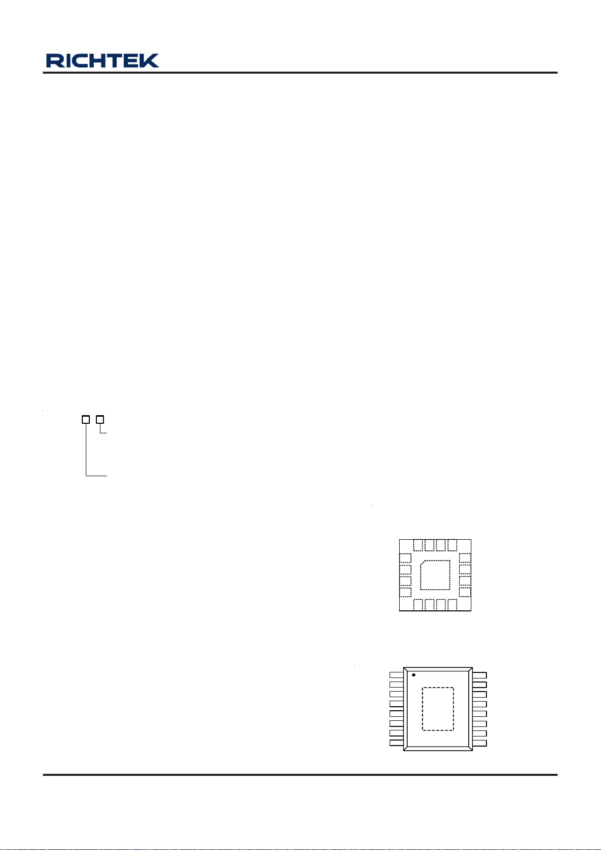
Pin Configurations
(TOP VIEW)
PGOOD
VDD
1516
COMP
1
FB
2
RT
SYNC
VDD
PGOOD
COMP
FB
RT
SYNC
EN/SS
GND
TSSOP-16 (Exposed Pad)
GND
3
4
GND
EN/SS
VQFN-16L 4x4
2
3
4
GND
5
6
7
8
14
17
PVDD
PVDD
17
13
LX
LX
12
PGND
11
PGND
10
LX
9
8765
LX
16
15
14
13
12
11
10
9
PVDD
LX
LX
PGND
PGND
LX
LX
PVDD
DS8004-07 March 2011 www.richtek.com
1
RT8004
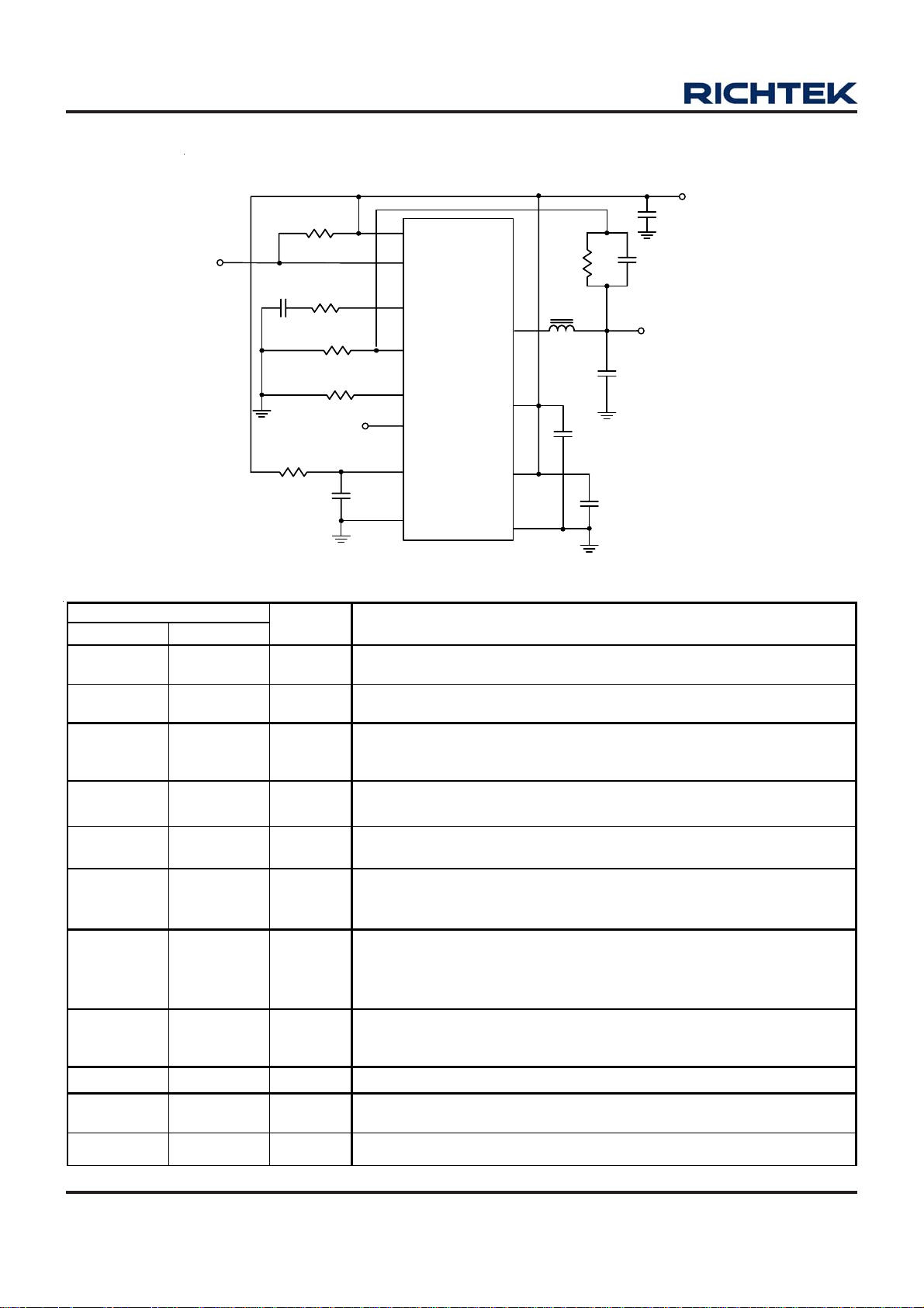
Typical Application Circuit
V
IN
2.65V to 5.5V
PGOOD
RPG
100k
CTH
1000pF
RTH
10k
External Clock
R
SS
4.7M
R2
240k
R
OCS
309k
C
SS
470pF
VDD
RT8004
PGOOD
COMP
FB
RT
SYNC
EN/SS
GND
LX
PVDD
PVDD
PGND
510k
L1
1uH
R1
C
IN1
10uF
C
IN2
10uF
C
OUT
47uF
47uF
C1
22pF
V
OUT
2.5V/3A
Functional Pin Description
Pin No.
RT8004PCP RT8004PQP
1 15 VDD
2 16 PGO OD
3 1 COMP
4 2 FB
5 3 RT
6 4 SYNC
7 5 EN/ SS
8,
Exposed Pad
(17)
6,
Exposed Pad
(17)
9, 16 7, 14 PVDD Power Input Supply. Decouple this pin to PGND with a capacitor.
10,11,
14, 15
8, 9, 12, 13 LX
Pin Name Pin Function
Signal Input Supply. Decouple this pin to GND with a capacitor.
Norm al ly VDD is equal to P VDD.
Power Good Indicator. Open-drain logic output that is pulled to ground
when the output voltage is not within ±12.5% of regulation point.
Error Amplifier Compensation Pin. The current comparator threshold
increases with this control voltage. Connect external compensation
elements to this pin to stabilize the control loop.
Feedback Pin. Receives the feedback voltage from a resistive divider
connected across the output.
Oscillator Resistor Input. Connecting a resistor to ground from this pin
sets the switching frequency.
External Clock Synchronization Input. The internal oscillator can be
synchronized to an external clock applied to this pin. If not use, please
connect this pin to VDD or GND.
Enable Control and Soft-Start Input. Forcing this pin below 0.5V shuts
down the RT8004. In shutdown all functions are disabled drawing < 1μA
of supply current. A capacitor to ground from this pin sets the ramp time
to full output current.
Signal Ground. All small-signal components, compensation components
GND
and the exposed pad on the bottom side of the IC should connect to this
ground, which in turn connects to PGND at one point.
Internal Power MOSFET Switches Output. Connect this pin to the
inductor.
12, 13 10, 11 PGND Power Ground. Connect this pin close to the terminal of CIN and C
DS8004-07 March 2011www.richtek.com
2
OUT
.
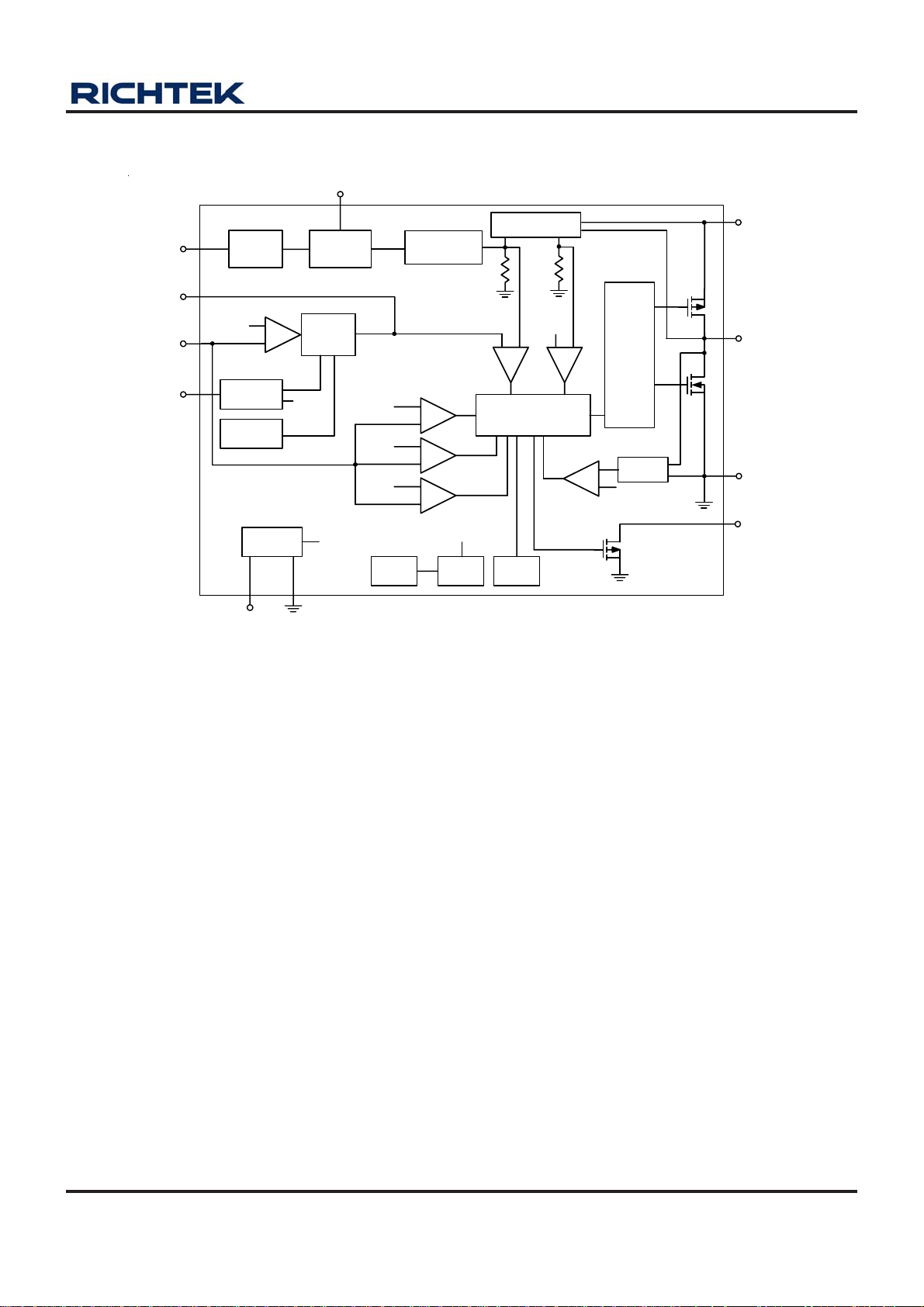
Function Block Diagram
RT8004
RT
SYNC
COMP
FB
EN/SS
ExtSyn
0.8V
Ext_SS
Int_SS
VDD
EA
POR
GND
SD
Oscillator
Output
Clamp
POR
0.9V
0.7V
0.4V
BG
Slope Com
0.8V
V
REF
Control
Logic
OTP
ISEN
OC
Limit
Driver
NISEN
NMOS I Limit
PVDD
LX
PGND
PGOOD
Operation
Main Control Loop
The RT8004 is a monolithic, constant-frequency, current mode step-down DC/DC converter. During normal operation,
the internal top power switch (P-MOSFET) is turned on at the beginning of each clock cycle. Current in the inductor
increases until the peak inductor current reach the value defined by the voltage on the COMP pin. The error amplifier
adjusts the voltage on the COMP pin by comparing the feedback signal from a resistor divider on the FB pin with an
internal 0.8V reference. When the load current increases, it causes a reduction in the feedback voltage relative to the
reference. The error amplifier raises the COMP voltage until the average inductor current matches the new load current.
When the top power MOSFET shuts off, the synchronous power switch (N-MOSFET) turns on until either the bottom
current limit is reached or the beginning of the next clock cycle. The bottom current limit is set at −2A.
The operating frequency is set by an external resistor connected between the RT pin and ground. The practical switching
frequency can range from 300kHz to 4MHz.
Power Good comparators will pull the PGOOD output low if the output voltage comes out of regulation by 12.5%. In an
over voltage condition, the top power MOSFET is turned off and the bottom power MOSFET is switched on until either
the overvoltage condition clears or the bottom MOSFET’ s current limit is reached.
Frequency Synchronization
The internal oscillator of the RT8004 can be synchronized to an external clock connected to the SYNC pin. The
frequency of the external clock can be in the range of 300kHz to 4MHz. For this application, the oscillator timing resistor
should be chosen to correspond to a frequency that is about 20% lower than the synchronization frequency.
DS8004-07 March 2011 www.richtek.com
3

RT8004
Dropout Operation
When the input supply voltage decreases toward the output voltage, the duty cycle increases toward the maximum on-
time. Further reduction of the supply voltage forces the main switch to remain on for more than one cycle eventually
reaching 100% duty cycle. The output voltage will then be determined by the input voltage minus the voltage drop across
the internal P-MOSFET and the inductor.
Low Supply Operation
The RT8004 is designed to operate down to an input supply voltage of 2.65V. One important consideration at low input
supply voltages is that the R
calculate the power dissipation when the RT8004 is used at 100% duty cycle with low input voltages to ensure that
thermal limits are not exceeded.
Slope Compensation and Inductor Peak Current
Slope compensation provides stability in constant frequency architectures by preventing subharmonic oscillations at
duty cycles greater than 50%. It is accomplished internally by adding a compensating ramp to the inductor current
signal. Normally, the maximum inductor peak current is reduced when slope compensation is added. In the RT8004,
however, separated inductor current signals are used to monitor over current condition and minimum peak current. This
keeps the maximum output current and minimum peak current relatively constant regardless of duty cycle.
of the P-MOSFET and N-MOSFET power switches increases. The user should
DS(ON)
Short Circuit Protection
When the output is shorted to ground, the inductor current decays very slowly during a single switching cycle. A current
runaway detector is used to monitor inductor current. As current increasing beyond the control of current loop, switching
cycles will be skipped to prevent current runaway from occurring.
DS8004-07 March 2011www.richtek.com
4
RT8004
Absolute Maximum Ratings (Note 1)
z Supply Input Voltage ---------------------------------------------------------------------------------------------- −0.3V to 6V
z LX Pin Switch Voltage -------------------------------------------------------------------------------------------- −0.3V to (PV
z Other I/O Pin Voltages ------------------------------------------------------------------------------------------- −0.3V to (V
z Power Dissipation, P
@ T
D
= 25°C
A
TSSOP-16 ----------------------------------------------------------------------------------------------------------- 2.66W
VQFN-16L 4x4 ----------------------------------------------------------------------------------------------------- 2.315W
z Package Thermal Resistance (Note 2)
TSSOP-16, θJA----------------------------------------------------------------------------------------------------- 47°C/W
VQFN-16L 4x4, θJA------------------------------------------------------------------------------------------------ 54°C/W
VQFN-16L 4x4, θJC----------------------------------------------------------------------------------------------- 7°C/W
z Lead Temperature (Soldering, 10 sec.)----------------------------------------------------------------------- 260°C
z Junction Temperature --------------------------------------------------------------------------------------------- 150°C
z Storage Temperature Range ------------------------------------------------------------------------------------ −65°C to +150°C
z ESD Susceptibility (Note 3)
HBM (Human Body Mode) -------------------------------------------------------------------------------------- 2kV
MM (Machine Mode) ---------------------------------------------------------------------------------------------- 200V
+ 0.3V)
DD
+ 0.3V)
DD
Recommended Operating Conditions (Note 4)
z Supply Input Voltage ---------------------------------------------------------------------------------------------- 2.65V to 5.5V
z Ambient Temperature Range ------------------------------------------------------------------------------------ −40°C to 85°C
z Junction Temperature Range ------------------------------------------------------------------------------------ −40°C to 125°C
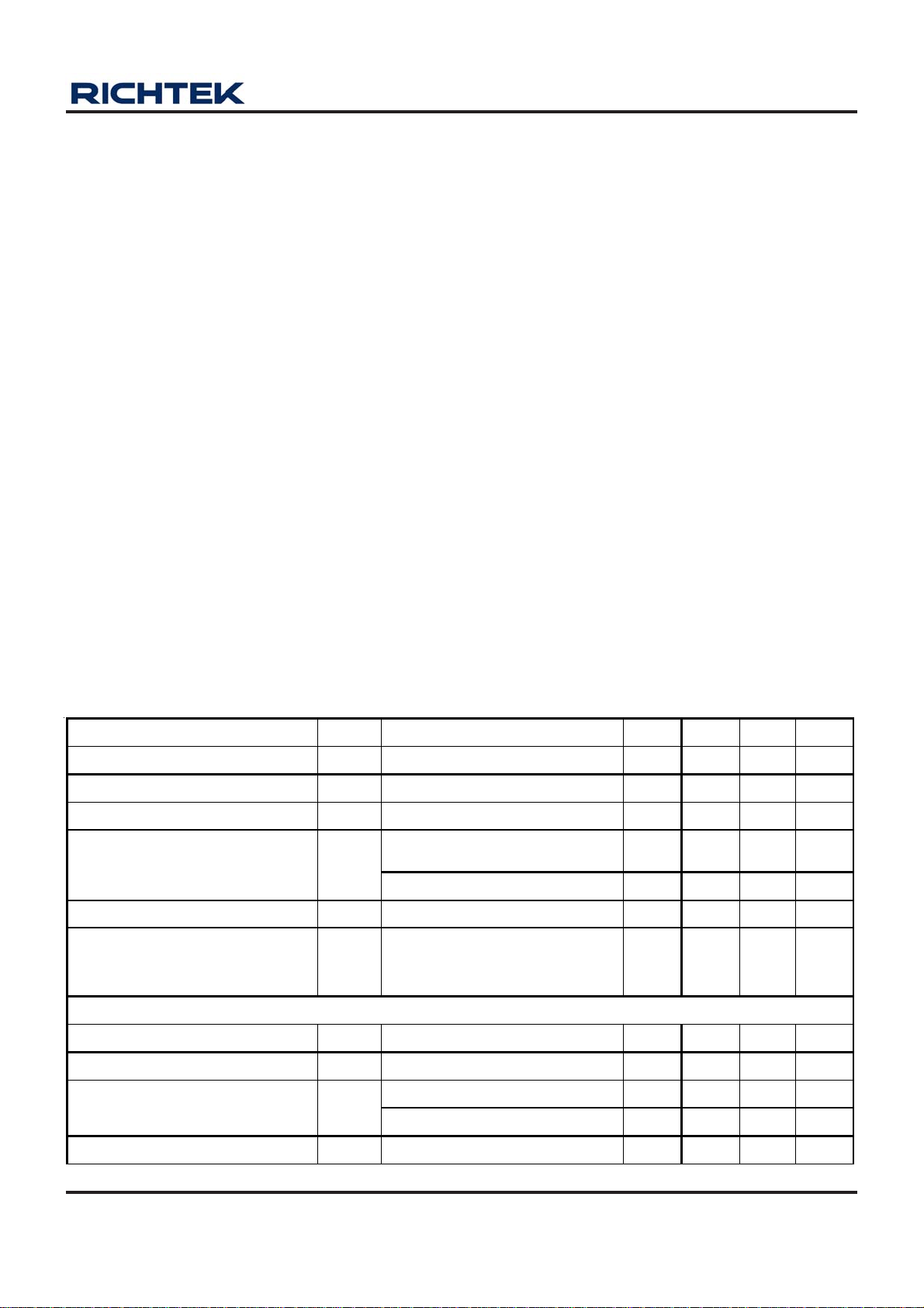
Electrical Characteristics
(V
= 3.3V, TA = 25°C, unless otherwise specified)
DD
Parameter Symbol Test Conditions Min Typ Max Unit
Input Voltage Range VDD 2.65 -- 5.5 V
Feedback Voltage VFB (Note 5) 0.784 0.8 0.816 V
Feedback Leakage Current IFB -- -- 0.4 μA
Input DC Bias Current
Reference Voltage Line Regulation V
Output Voltage Load Regulation
Power Good
Active, V
Not switching
Shutdown, V
= 2.7V to 5.5V (Note 5) -- 0.04 0.5 %/V
IN
Measured in Servo Loop,
V
COMP
(Note 5)
= 0.78V,
FB
< 0.1V (Note 5) -- -- 1 μA
EN
= 1.2V to 1.6V
180 400 520 μA
-- 0.05 +/-0.2 %
Power Good Range -- ±12.5 ±15 %
Power Good Pull-Down Resistance -- -- 120 Ω
R
= 309k 0.8 1 1.2 MHz
Switching Frequency f
OSC
OSC
Switching Frequency Range 0.3 -- 4 MHz
Sync Frequency Range (Note 6) 0.3 -- 4 MHz
To be continued
DS8004-07 March 2011 www.richtek.com
5

RT8004
Parameter Symbol Test Conditions Min Typ Max Unit
Switch On Resistance, High R
Switch On Resistance, Low R
Peak Curr en t L im it I
Under Voltage Lockout Threshold
PFET
NFET
LIM
I
= 1A
SW
I
= 1A
SW
45 75 110
mΩ
45 69 100 mΩ
4 5.2 -- A
VDD Rising 2.25 2.52 2.7 V
Hysteresis -- 0.15 -- V
SW Leakage Current
V
= 0V, VIN = 5.5V
EN
EN/SS Leakage Current -- -- 1
Enable Threshold
Note 1. Stresses listed as the above “Absolute Maximum Ratings” may cause permanent damage to the device. These are for
stress ratings. Functional operation of the device at these or any other conditions beyond those indicated in the
operational sections of the specifications is not implied. Exposure to absolute maximum rating conditions for extended
periods may remain possibility to affect device reliability.
Note 2. θ
Note 3. Devices are ESD sensitive. Handling precaution recommended.
Note 4. The device is not guaranteed to function outside its operating conditions.
Note 5. The specifications over the -40°C to 85°C operation ambient temperature range are assured by design, characterization
Note 6. The external synchronous frequency must be equal to 1 to 1.3 times of the internal setting frequency. The switching
is measured in the natural convection at TA = 25°C on 4-layers high effective thermal conductivity test board of
JA
JEDEC 51-7 thermal measurement standard. The measurement case position of θ
package.
and correlation with statistical process controls.
frequency range is guaranteed by design but not production tested.
V
EN
0.65 -- 0.95 V
-- - - 1 μA
μA
is on the exposed pad of the
JC
DS8004-07 March 2011www.richtek.com
6

Typical Operating Characteristics
RT8004
100%
100
90
90%
80
80%
70%
70
60%
60
50
50%
40
40%
Efficiency (%)
30
30%
20%
20
10
10%
0%
V
OUT
(1V/Div)
Efficiency vs. Output Current
VIN = 5V
VIN = 3.3V
V
= 2.5V, 1M Continuous Mode Operation
0
0 500 1000 1500 2000 2500 3000
OUT
Output Current (mA)
Soft-Start Power On
VIN = 3.3V, V
R
= 0.83Ω
LOAD
OUT
= 2.5V
0.30%
0.30
0.20%
0.20
0.10%
0.10
0.00%
Deviation (%)
OUT
V
-0.10%
-0.10
-0.20%
-0.20
I
L
(2A/Div)
Load Regulation
VIN = 3.3V, V
0
50 550 1050 1550 2050 2550 3050
= 2.5V
OUT
Output Current (mA)
Power Off
VIN = 3.3V, V
OUT
= 2.5V, I
OUT
= 0A
V
SS
(1V/Div)
I
L
(1A/Div)
V
OUT
(10mV/Div)
V
LX
(2V/Div)
I
L
(2A/Div)
VIN = 3.3V, V
Time (2.5ms/Div)
Ripple Voltage
= 2.5V, I
OUT
OUT
= 3A
V
OUT
(2V/Div)
V
LX
(5V/Div)
V
IN
(2V/Div)
V
OUT
(50mV/Div)
I
L
(1A/Div)
Time (25ms/Div)
Load Transient Response
VIN = 3.3V, V
I
= No Load to 3A
LOAD
OUT
= 2.5V
Time (500ns/Div)
Time (25μs/Div)
DS8004-07 March 2011 www.richtek.com
7

RT8004
)
Deviation (%)
-0.50%
REF
V
-1.00%
-1.50%
Frequency (MHz)
V
Deviation vs. Temperature
1.50%
1.00%
0.50%
0.00%
-50 -25 0 25 50 75 100 125
REF
VIN = 3.3V
Temperature (°C)
Frequency vs. Input Voltage
1.04
R = 309k
1.032
1.024
1.016
1.008
1
0.992
3 3.5 4 4.5 5 5.5
Input Voltage (V)
Frequency vs. R
4500
4000
3500
3000
2500
2000
1500
RT
Frequency (kHz)
1000
500
0
0 200 400 600 800 1000 1200 1400
RRT (kٛ)
(kΩ)
Frequency vs. Temperature
5
5
VIN = 3.3V
4
4
3
3
2
2
1
1
0
0
-1
-1
-2
-2
-3
-3
Frequency Deviation (%) 1
-4
-4
-5
-5
-50 -25 0 25 50 75 100 125
Temperature (°C)
VIN = 3.3V
Quiescent Current vs . Input Voltage
500
450
400
350
300
250
200
150
Quiescent Current (μA
100
50
0
3 3.5 4 4.5 5 5.5
Input Voltage (V)
Peak Current Limited vs. Input Voltage
5.5
V
= 2.5V
OUT
5.3
5.1
4.9
4.7
Peak Current Limited (A)
4.5
33.544.555.5
Input Voltage (V)
DS8004-07 March 2011www.richtek.com
8
Application Information
RT8004
The basic RT8004 application circuit is shown in Typical
Application Circuit. External component selection is
determined by the maximum load current and begins with
the selection of the inductor value and operating frequency
followed by CIN and C
OUT
.
Operating Frequency
Selection of the operating frequency is a tradeoff between
efficiency and component size. High frequency operation
allows the use of smaller inductor and capacitor values.
Operation at lower frequencies improves efficiency by
reducing internal gate charge and switching losses but
requires larger inductance values and/or capacitance to
maintain low output ripple voltage.
The operating frequency of the RT8004 is determined by
an external resistor that is connected between the RT pin
and ground. The value of the resistor sets the ramp current
that is used to charge and discharge an internal timing
capacitor within the oscillator. The RT resistor value can
be determined by examining the frequency vs. R
RT
curve.
Although frequencies as high as 4MHz are possible, the
minimum on-time of the RT8004 imposes a minimum limit
on the operating duty cycle. The minimum on-time is
typically 110ns. Therefore, the minimum duty cycle is
equal to 100 x 110ns x f(Hz).
Inductor Selection
For a given input and output voltage, the inductor value
and operating frequency determine the ripple current. The
ripple current ΔIL increases with higher VIN and decreases
with higher inductance.
ΔI
V
⎡
=
L
⎢
⎣
⎡
⎤
−
1
⎢
⎥
×
Lf
⎦
⎣
⎤
V
OUTOUT
⎥
V
IN
⎦
Having a lower ripple current reduces the ESR losses in
the output capacitors and the output voltage ripple. Highest
efficiency operation is achieved at low frequency with small
ripple current. This, however, requires a large inductor.
A reasonable starting point for selecting the ripple current
is ΔIL = 0.4(I
). The largest ripple current occurs at the
MAX
highest VIN. To guarantee that the ripple current stays
below a specified maximum, the inductor value should be
chosen according to the following equation :
⎡
V
⎡
L
=
OUT
⎢
L(MAX)
If
Δ×
⎣
V
⎤
1
−
⎢
⎥
V
⎦
⎢
IN(MAX)
⎣
OUT
⎤
⎥
⎥
⎦
Inductor Core Selection
Once the value for L is known, the type of inductor must
be selected. High efficiency converters generally cannot
afford the core loss found in low cost powdered iron cores,
forcing the use of more expensive ferrite or mollypermalloy
cores. Actual core loss is independent of core size for a
fixed inductor value but it is very dependent on the
inductance selected. As the inductance increases, core
losses decrease. Unfortunately, increased inductance
requires more turns of wire and therefore copper losses
will increase.
Ferrite designs have very low core losses and are preferred
at high switching frequencies, so design goals can
concentrate on copper loss and preventing saturation.
Ferrite core material saturates “hard”, which means that
inductance collapses abruptly when the peak design
current is exceeded. This results in an abrupt increase in
inductor ripple current and consequent output voltage ripple.
Do not allow the core to saturate!
Different core materials and shapes will change the size/
current and price/current relationship of an inductor.
Toroid or shielded pot cores in ferrite or permalloy materials
are small and don’t radiate energy but generally cost
more than powdered iron core inductors with similar
characteristics. The choice of which style inductor to use
mainly depends on the price vs size requirements and
any radiated field/EMI requirements.
CIN and C
Selection
OUT
The input capacitance, CIN, is needed to filter the
trapezoidal current at the source of the top MOSFET. To
prevent large ripple voltage, a low ESR input capacitor
sized for the maximum RMS current should be used. RMS
current is given by :
V
II
OUT(MAX)RMS
OUT
V
V
IN
1
−=
V
OUT
IN
DS8004-07 March 2011 www.richtek.com
9

RT8004
This formula has a maximum at VIN = 2V
IRMS = I
/2. This simple worst-case condition is
OUT
OUT
, where
commonly used for design because even significant
deviations do not offer much relief. Note that ripple current
ratings from capacitor manufacturers are often based on
only 2000 hours of life which makes it advisable to further
derate the capacitor, or choose a capacitor rated at a higher
temperature than required. Several capacitors may also
be paralleled to meet size or height requirements in the
design.
The selection of C
is determined by the effective series
OUT
resistance (ESR) that is required to minimize voltage ripple
and load step transients, as well as the amount of bulk
capacitance that is necessary to ensure that the control
loop is stable. Loop stability can be checked by viewing
the load transient response as described in a later section.
The output ripple, ΔV
⎡
ESR ΔIΔV
LOUT
⎢
⎣
, is determined by :
OUT
1
OUT
⎤
⎥
⎦
+≤
8fC
The output ripple is highest at maximum input voltage
since ΔIL increases with input voltage. Multiple capacitors
placed in parallel may be needed to meet the ESR and
RMS current handling requirements. Dry tantalum, special
polymer, aluminum electrolytic and ceramic capacitors are
all available in surface mount packages. Special polymer
capacitors offer very low ESR but have lower capacitance
density than other types. Tantalum capacitors have the
highest capacitance density but it is important to only
use types that have been surge tested for use in switching
power supplies. Aluminum electrolytic capacitors have
significantly higher ESR but can be used in cost-sensitive
applications provided that consideration is given to ripple
current ratings and long term reliability. Ceramic capacitors
have excellent low ESR characteristics but can have a
high voltage coefficient and audible piezoelectric effects.
The high Q of ceramic capacitors with trace inductance
can also lead to significant ringing.
be taken when these capacitors are used at the input and
output. When a ceramic capacitor is used at the input
and the power is supplied by a wall adapter through long
wires, a load step at the output can induce ringing at the
input, VIN. At best, this ringing can couple to the output
and be mistaken as loop instability. At worst, a sudden
inrush of current through the long wires can potentially
cause a voltage spike at VIN large enough to damage the
part.
Output Voltage Programming
The output voltage is set by an external resistive divider
according to the following equation :
R2
0.8V(1VOUT +=
)
R1
The resistive divider allows the VFB pin to sense a fraction
of the output voltage as shown in Figure 1.
V
OUT
R2
VFB
RT8004
GND
Figure 1. Setting the Output Voltage
Frequency Synchronization
The RT8004’ s internal oscillator can be synchronized to
an external clock signal. During synchronization, the top
MOSFET turn-on is locked to the falling edge of the
external frequency source. The synchronization frequency
range is 300kHz to 4MHz. Synchronization only occurs if
the external frequency is greater than the frequency set
by the external resistor. Because slope compensation is
generated by the oscillator’ s RC circuit, the external
frequency should be set 25% higher than the frequency
set by the external resistor to ensure that adequate slope
compensation is present.
R1
Using Ceramic In put and Output Capacitors
Higher values, lower cost ceramic capacitors are now
becoming available in smaller case sizes. Their high ripple
current, high voltage rating and low ESR make them ideal
for switching regulator applications. However, care must
10
Soft-Start
The EN/SS pin provides a means to shut down the RT8004
as well as a timer for soft-start. Pulling the EN/SS pin
below 0.5V places the RT8004 in a low quiescent current
shutdown state (IQ < 1μA).
DS8004-07 March 2011www.richtek.com

RT8004
The RT8004 contains an internal soft-start clamp that
gradually raises the clamp on COMP after the EN/SS pin
is pulled above 0.8V. The full current range becomes
available on COMP after 1024 switching cycles. If a longer
soft-start period is desired, the clamp on COMP can be
set externally with a resistor and capacitor on the EN/SS
pin as shown in Typical Application Circuit. The soft-start
duration can be calculated by using the following formula:
IN
=
SSSSSS
V
ln( x C x RT
IN
−
(s) )
1.8VV
Efficiency Considerations
The efficiency of a switching regulator is equal to the output
power divided by the input power times 100%. It is often
useful to analyze individual losses to determine what is
limiting the efficiency and which change would produce
the most improvement. Efficiency can be expressed as:
Efficiency = 100% − (L1+ L2+ L3+ ...)
where L1, L2, etc. are the individual losses as a percentage
of input power. Although all dissipative elements in the
circuit produce losses, two main sources usually account
for most of the losses: VDD quiescent current and I2R
losses. The VDD quiescent current loss dominates the
efficiency loss at very low load currents whereas the I2R
loss dominates the efficiency loss at medium to high load
currents. In a typical efficiency plot, the efficiency curve
at very low load currents can be misleading since the
actual power lost is of no consequence.
1. The VDD quiescent current is due to two components:
the DC bias current as given in the electrical characteristics
and the internal main switch and synchronous switch gate
charge currents. The gate charge current results from
switching the gate capacitance of the internal power
MOSFET switches. Each time the gate is switched from
high to low to high again, a packet of charge ΔQ moves
from VDD to ground. The resulting ΔQ/Δt is the current out
of VDD that is typically larger than the DC bias current. In
continuous mode,
I
GATECHG
= f(QT+QB)
losses are proportional to VDD and thus their effects will
be more pronounced at higher supply voltages.
2. I2R losses are calculated from the resistances of the
internal switches, RSW and external inductor RL. In
continuous mode the average output current flowing
through inductor L is “chopped” between the main switch
and the synchronous switch. Thus, the series resistance
looking into the LX pin is a function of both top and bottom
MOSFET R
RSW = R
The R
DS(ON)TOP
DS(ON)
and the duty cycle (DC) as follows :
DS(ON)
x DC + R
DS(ON)BOT
x (1−DC)
for both the top and bottom MOSFETs can be
obtained from the Typical Performance Characteristics
curves. Thus, to obtain I2R losses, simply add RSW to R
and multiply the result by the square of the average output
current.
Other losses including CIN and C
ESR dissipative
OUT
losses and inductor core losses generally account for less
than 2% of the total loss.
Thermal Considerations
In most applications, the RT8004 does not dissipate much
heat due to its high efficiency. But, in applications where
the RT8004 is running at high ambient temperature with
low supply voltage and high duty cycles, such as in
dropout, the heat dissipated may exceed the maximum
junction temperature of the part. If the junction temperature
reaches approximately 150°C, both power switches will
be turned off and the SW node will become high
impedance. To avoid the RT8004 from exceeding the
maximum junction temperature, the user will need to do
some thermal analysis. The goal of the thermal analysis
is to determine whether the power dissipated exceeds
the maximum junction temperature of the part. The
temperature rise is given by :
TR = PD x θ
JA
Where PD is the power dissipated by the regulator and
θJA is the thermal resistance from the junction of the die
to the ambient temperature. The junction temperature, TJ,
is given by :
L
where QT and QB are the gate charges of the internal top
and bottom switches. Both the DC bias and gate charge
DS8004-07 March 2011 www.richtek.com
TJ = TA + T
R
Where TA is the ambient temperature.
11

RT8004
As an example, consider the RT8004 in dropout at an
input voltage of 3.3V, a load current of 3A and an ambient
temperature of 70°C. From the typical performance graph
of switch resistance, the R
of the P-Channel switch
DS(ON)
at 70°C is approximately 97mΩ. Therefore, power
dissipated by the part is :
PD = (I
LOAD
)2 (R
) = (3A)2 (97mΩ) = 0.873W
DS(ON)
For the TSSOP package, the θJA is 47°C/W. Thus the
junction temperature of the regulator is :
TJ = 70°C+(0.873W) (47°C/W) = 111°C
Which is below the maximum junction temperature of
125°C. Note that at higher supply voltages, the junction
temperature is lower due to reduced switch resistance
(R
DS(ON)
).
Checking Tra n sient Re spon se
The regulator loop response can be checked by looking
at the load transient response. Switching regulators take
several cycles to respond to a step in load current. When
a load step occurs, V
equal to ΔI
resistance of C
discharge C
(ESR), where ESR is the effective series
LOAD
OUT
generating a feedback error signal used
OUT
by the regulator to return V
During this recovery time, V
immediately shifts by an amount
OUT
. ΔI
also begins to charge or
LOAD
to its steady-state value.
OUT
can be monitored for
OUT
overshoot or ringing that would indicate a stability problem.
The COMP pin external components and output capacitor
shown in Typical Application Circuit will provide adequate
compensation for most applications.
_ LX node is with high frequency voltage swing and should
be kept small area. Keep all sensitive small-signal nodes
away from LX node to prevent stray capacitive noise
pick-up.
_ Flood all unused areas on all layers with copper.
Flooding with copper will reduce the temperature rise
of power components. You can connect the copper areas
to any DC net (PVIN, SVIN, V
, PGND, SGND, or
OUT
any other DC rail in your system).
_ Connect the FB pin directly to the feedback resistors.
The resistor divider must be connected between V
OUT
and GND.
Layout Considerations
Follow the PCB layout guidelines for optimal performance
of RT8004.
_ A ground plane is recommended. If a ground plane layer
is not used, the signal and power grounds should be
segregated with all small-signal components returning
to the GND pin at one point that is then connected to
the PGND pin close to the IC. The exposed pad should
be connected to GND.
_ Connect the terminal of the input capacitor(s), C
IN
, as
close as possible to the PVDD pin. This capacitor
provides the AC current into the internal power
MOSFETs.
12
DS8004-07 March 2011www.richtek.com

Outline Dimension
RT8004
D
L
EXPOSED THERMAL PAD
(Bottom of Package)
E
A
b
U
E1
V
e
A2
A1
Dimensions In Millimeters Dimensions In Inches
Symbol
Min Max Min Max
A 1.000 1.200 0.039 0.047
A1 0.000 0.150 0.000 0.006
A2 0.800 1.050 0.031 0.041
b 0.190 0.300 0.007 0.012
D 4.900 5.100 0.193 0.201
e 0.65 0.026
E 6.300 6.500 0.248 0.256
E1 4.300 4.500 0.169 0.177
L 0.450 0.750 0.018 0.030
U 2.000 3.000 0.079 0.118
V 2.000 3.000 0.079 0.118
16-Lead TSSOP (Exposed Pad) Plastic Package
DS8004-07 March 2011 www.richtek.com
13

RT8004
D
D2
L
SEE DETAIL A
1
E
e
A
A3
A1
E2
1
2
b
DETAIL A
1
2
Pin #1 ID and Tie Bar Mark Options
Note : The configuration of the Pin #1 identifier is optional,
but must be located within the zone indicated.
Dimensions In Millimeters Dimensions In Inches
Symbol
Min Max Min Max
A 0.800 1.000 0.031 0.039
A1 0.000 0.050 0.000 0.002
A3 0.175 0.250 0.007 0.010
b 0.250 0.380 0.010 0.015
D 3.950 4.050 0.156 0.159
D2 2.000 2.450 0.079 0.096
E 3.950 4.050 0.156 0.159
E2 2.000 2.450 0.079 0.096
e 0.650 0.026
L 0.500 0.600
Richtek Technology Corporation
Headquarter
5F, No. 20, Taiyuen Street, Chupei City
Hsinchu, Taiwan, R.O.C.
Tel: (8863)5526789 Fax: (8863)5526611
0.020 0.024
V-Type 16L VQFN 4x4 Package
Richtek Technology Corporation
Taipei Office (Marketing)
5F, No. 95, Minchiuan Road, Hsintien City
Taipei County, Taiwan, R.O.C.
Tel: (8862)86672399 Fax: (8862)86672377
Email: marketing@richtek.com
Information that is provided by Richtek Technology Corporation is believed to be accurate and reliable. Richtek reserves the right to make any change in circuit
design, specification or other related things if necessary without notice at any time. No third party intellectual property infringement of the applications should be
guaranteed by users when integrating Richtek products into any application. No legal responsibility for any said applications is assumed by Richtek.
DS8004-07 March 2011www.richtek.com
14

 Loading...