

RT9163
500mA Low Dropout Positive Voltage Regulator
General Description
The RT9163 is a positive low dropout regulator
designed for applications requiring low dropout
performance at full rated current. The device is
available in fixed output voltage of 3.3V, 3.5V, and
5.0V. The RT9163 provides excellent regulation over
line, load, and temperature variations.
The other features include low dropout performance
at a maximum of 1.4V at 500mA, fast transient
response, internal current limiting, and thermal
shutdown protection of the output devices. The
RT9163 is a three-terminal regulator available in
surface mount SOT-89, SOT-223, and TO-252
packages.
Applications
5V to 3.3V Linear Regulator
z
Low Voltage Microcontroller, DSP… etc Power
z
Supply
Linear Regulator for LAN Card and CD-ROM
z
Ordering Information
RT9163-
Package type
ZL : TO-92
X : SOT-89
XL : SOT-89, L Type
L : TO-252
G : SOT-223 Type I
GL : SOT-223 Type II
GT : SOT-223 Type III
GF : SOT-223 Type IV
Operating temperature range
C: Commercial standard
Output voltage
33 : 3.3V
35 : 3.5V
50 : 5.0V
Features
z
Low Dropout, Maximum 1.4V at 500mA
z
Fast Transient Response
z ±
±2% Total Output Regulation
±±
z
0.4% Line Regulation
z
0.4% Load Regulation
z
TO-92, SOT-89, SOT-223, and TO-252 Packages
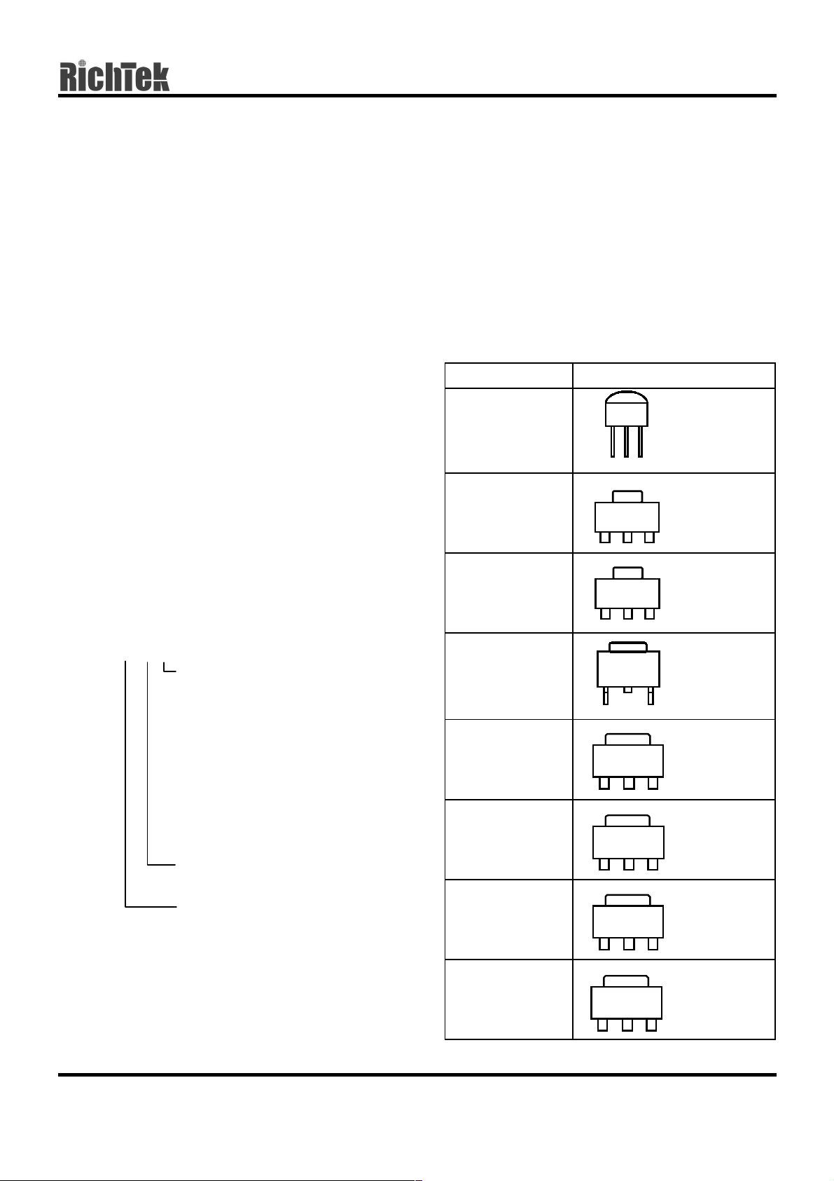
Pin Configurations
Part Number Pin Configurations
RT9163-CZL
(Plastic TO-92)
RT9163-CX
(Plastic SOT-89)
RT9163-CXL
(Plastic SOT-89)
RT9163-CL
(Plastic TO-252)
RT9163-CG
(Plastic SOT-223)
Type I
RT9163-CGL
(Plastic SOT-223)
Type II
RT9163-CGT
(Plastic SOT-223)
Type III
RT9163-CGF
(Plastic SOT-223)
Type IV
123
123
123
123
123
123
123
123
TOP VIEW
1. VIN
2. GND
3.
VOUT
TOP VIEW
1. VOUT
2. GND (TAB)
3.
VIN
TOP VIEW
1. GND
2. VIN (TAB)
3.
VOUT
TOP VIEW
1. VOUT
2. GND (TAB)
3.
VIN
TOP VIEW
1. VOUT
2. GND (TAB)
3.
VIN
TOP VIEW
1. VIN
2. GND (TAB)
3.
VOUT
TOP VIEW
1. GND
2. VOUT (TAB)
3.
VIN
TOP VIEW
1. GND
2. VIN (TAB)
3.
VOUT
DS9163-14 April 2002 www.richtek-ic.com.tw
1
RT9163
Marking Information
Part Number Marking
RT9163-33CZL RTAJ
RT9163-35CZL RTAK
RT9163-50CZL RTA1
RT9163-33CX A8
RT9163-35CX A9
RT9163-50CX AT
RT9163-33CXL CK
RT9163-35CXL CL
RT9163-50CXL CM
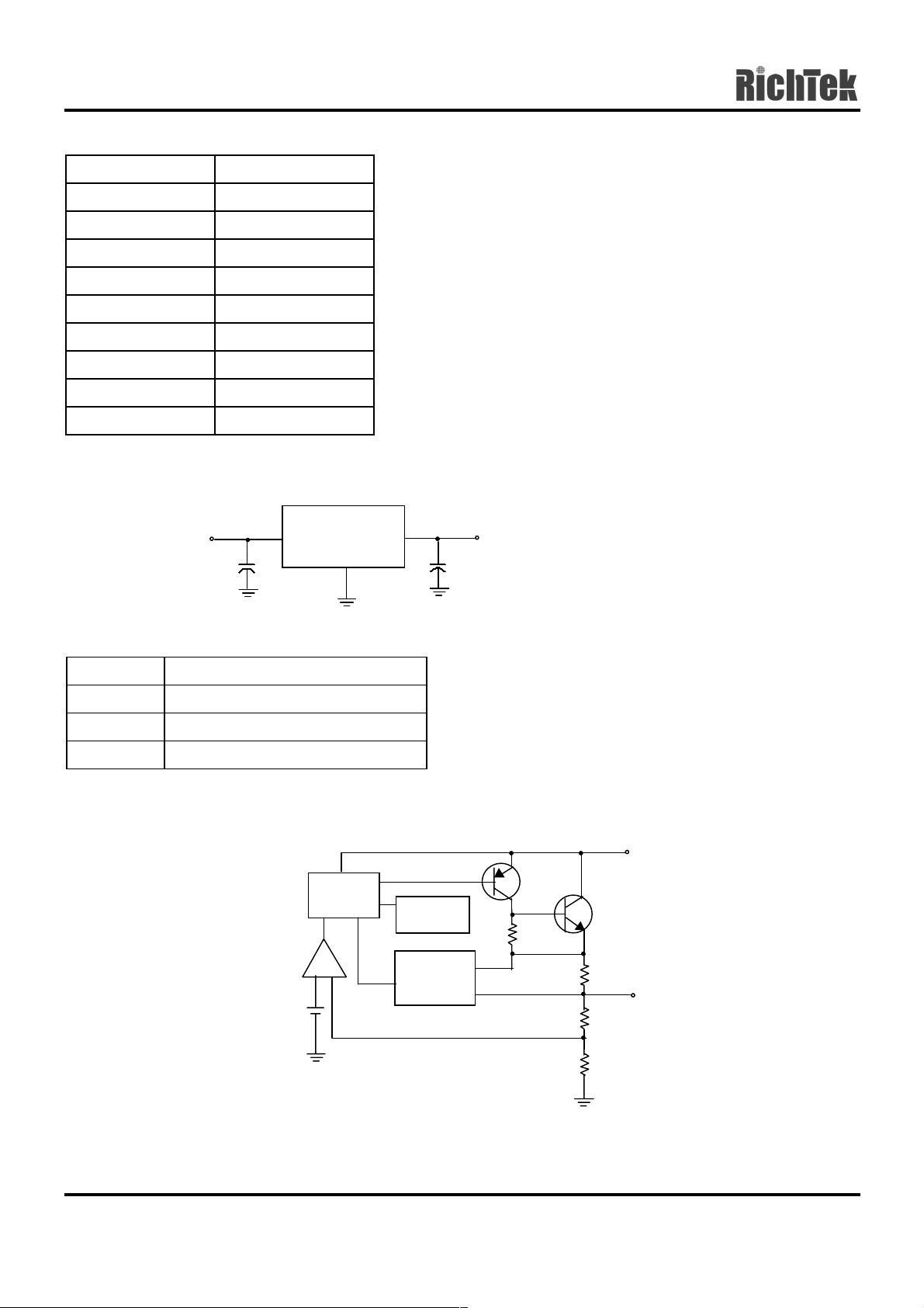
Typical Application Circuit
RT9163
V
IN
C1
10µF
VIN
+
_
GND
VOUT
+
_
C2
10µF
V
OU T
Pin Description
Pin Name Pin Function
VOUT Output Voltage
GND Ground
VIN Power Input
Function Block Diagram
Error
Amplifier
V
REF
Buffer
Amplifier
_
+
Thermal
Shutdown
Current
Limit ing
Sensor
Q2
R4
Q1
R3
R1
R2
V
IN
V
OU T
www.richtek-ic.com.tw DS9163-14 April 2002
2
RT9163
Absolute Maximum Ratings
Input Voltage 15V
z
Power Dissipation, PD @ TA = 25°C
z
TO-92 0.6W
SOT-89 0.5W
Package Thermal Resistance
z
TO-92, θ
SOT-89, θ
SOT-89, θ
SOT-223, θ
SOT-223, θ
TO-252, θ
TO-252, θ
Operating Junction Temperature Range −40°C to 125°C
z
Storage Temperature Range −65°C to 150°C
z
JA
JC
JA
JC
JA
15°C/W
JC
56°C/W
JA
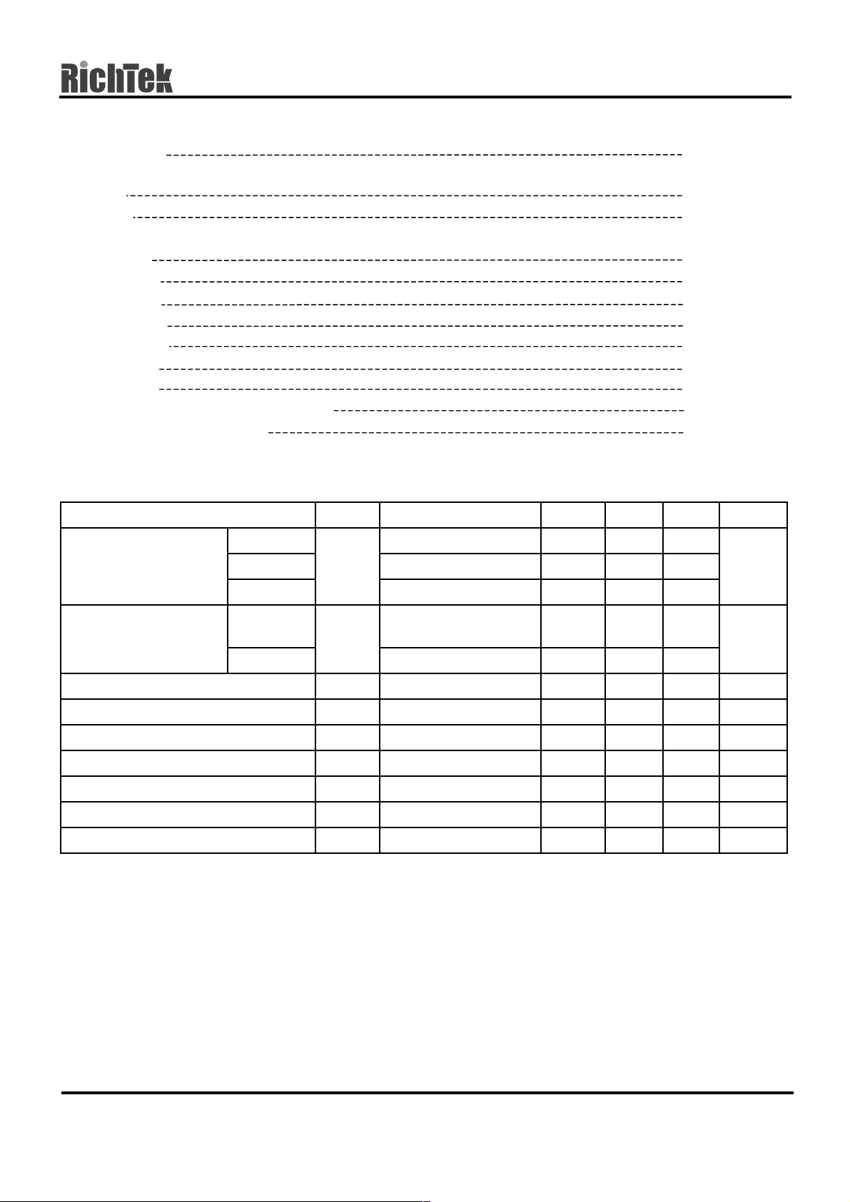
Electrical Characteristics
(V
= 5V, TA = 25°C, unless otherwise specified)
IN
Parameter Symbol Test Conditions Min Typ Max Units
160°C/W
100°C/W
300°C/W
15°C/W
60°C/W
RT9163-33 3.235 3.300 3.365
(1)
Line Regulation
Load Regulation
Dropout Voltage
(1)
(1)
(2)
Current Limit I
Quiescent Current I
Temperature Coefficient T
Temperature Stability T
RMS Output Noise
(3)
RT9163-35 3.430 3.500 3.570Output Voltage
RT9163-50
RT9163-33
RT9163-35
RT9163-50
V
OUT
∆V
LINE
∆V
LOADIL
V
DROP
LIMIT
Q
C
S
V
VIN = 7A 4.900 5.000 5.100
V
= 5V ~ 15V -- 0.1 0.4
IN
%
VIN = 7V ~ 15V -- 0.1 0.4
= 0 ~ 500mA -- 0.2 0.4 %
= 1% -- 1.3 1.4 V
∆V
OUT
Load = 1Ω 550 -- -- mA
-- 4.5 8 mA
-- 0.005 -- %/°C
-- 0.5 -- %
-- 0.003 -- %/V
OUT
Notes:
(1) Low duty cycle pulse tested with Kelvin connections.
(2) Dropout voltage is defined as the input to output differential at which the output voltage drops 100mV below the
value measured with a 1V differential.
(3) Bandwidth of 10 Hz to 10 kHz.
DS9163-14 April 2002 www.richtek-ic.com.tw
3

RT9163
Package Information
D
A
E
L
b
e
e
D1
A1
C
Dimensions In Millimeters Dimensions In Inches
Symbol
Min Max Min Max
A 3.175 4.191 0.125 0.165
A1 1.143 1.372 0.045 0.054
b 0.406 0.533 0.016 0.021
C 0.406 0.533 0.016 0.021
D 4.445 5.207 0.175 0.205
D1 3.429 -- 0.135 --
E 4.318 5.334 0.170 0.210
e 1.143 1.397 0.045 0.055
L 12.700 -- 0.500 --
3-Lead TO-92 Package
www.richtek-ic.com.tw DS9163-14 April 2002
4

RT9163
D
D1
C
C1
e e
b
b1 b
B
A
A
H
Symbol
Dimensions In Millimeters Dimensions In Inches
Min Max Min Max
A 1.397 1.600 0.055 0.063
b 0.356 0.483 0.014 0.019
B 2.388 2.591 0.094 0.102
b1 0.406 0.533 0.016 0.021
C -- 4.242 -- 0.167
C1 0.787 1.194 0.031 0.047
D 4.394 4.597 0.173 0.181
D1 1.397 1.753 0.055 0.069
e 1.448 1.549 0.057 0.061
H 0.355 0.432 0.014 0.017
3-Lead SOT-89 Surface Mount
DS9163-14 April 2002 www.richtek-ic.com.tw
5

RT9163
D
B
D1
E
L3
b1
b
e
U
V
A
C
L1
L2
b2
Symbol
Dimensions In Millimeters Dimensions In Inches
Min Max Min Max
A 2.184 2.388 0.086 0.094
B 0.889 2.032 0.035 0.080
b 0.508 0.889 0.020 0.035
b1 1.016 Ref. 0.040 Ref.
b2 0.457 0.584 0.018 0.023
C 0.457 0.584 0.018 0.023
D 6.350 6.731 0.250 0.265
D1 5.207 5.461 0.205 0.215
E 5.334 6.223 0.210 0.245
e 2.108 2.438 0.083 0.096
L1 9.398 10.414 0.370 0.410
L2 0.508 -- 0.020 --
L3 0.635 1.016 0.025 0.040
U 3.810 Ref. 0.150 Ref.
V 3.048 Ref. 0.120 Ref.
3-Lead TO-252 Plastic Surface Mount Package
www.richtek-ic.com.tw DS9163-14 April 2002
6

RT9163
D
D1
C
L
e
A A1
Dimensions In Millimeters Dimensions In Inches
Symbol
A -- 1.803 -- 0.071
A1 0.020 0.100
b 0.610 0.787 0.024 0.031
e
b
Min Max Min Max
B
0.0008
H
0.0047
B 3.302 3.708 0.130 0.146
C 6.706 7.290 0.264 0.287
D 6.299 6.706 0.248 0.264
D1 2.896 3.150 0.114 0.124
e 2.261 2.362 0.089 0.093
H 0.229 0.330 0.009 0.013
L 0.914 -- 0.036 --
3-Lead SOT-223 Plastic Surface Mount
DS9163-14 April 2002 www.richtek-ic.com.tw
7

RT9163
RICHTEK TECHNOLOGY CORP.
Headquarter
6F, No. 35, Hsintai Road, Chupei City
Hsinchu, Taiwan, R.O.C.
Tel: (8863)5510047 Fax: (8863)5537749
www.richtek-ic.com.tw DS9163-14 April 2002
RICHTEK TECHNOLOGY CORP.
Taipei Office (Marketing)
8F-1, No. 137, Lane 235, Paochiao Road, Hsintien City
Taipei County, Taiwan, R.O.C.
Tel: (8862)89191466 Fax: (8862)89191465
Email: marketing@richtek-ic.com.tw
8
 Loading...