


Richtek RT9293A-20GJ6, RT9293A-20GQWA, RT9293AGJ6, RT9293AGQW, RT9293AGQWA Schematic [ru]
...
RT9293
Small Package, High Performance, Asynchronies Boost
for 10 WLED Driver
General Description
The RT9293 is a high frequency, asynchronous boost
converter. The internal MOSFET can support up to 10
White LEDs for backlighting a nd OLED power application,
and the internal soft start function ca n reduce the inrush
current. The device operates with 1-MHz fixed switching
frequency to allow small external components and to
simplify possible EMI problems. For the protection, the
RT9293A provides 50V OVP a nd the RT9293B provides
50V/20V OVP to allow inexpensive and small-output
cap acitors with lower voltage ratings. The LED current is
initially set with the external sense resistor R
SET
. The
RT9293 is available in the tiny pa ckage type TSOT -23-6
and WDFN-8L 2x2 pa ckages to provide the best solution
for PCB space saving and total BOM cost.
Ordering Information
-
RT9293
Note :
Richtek products are :
` RoHS compliant and compatible with the current require-
ments of IPC/JEDEC J-STD-020.
` Suitable for use in SnPb or Pb-free soldering processes.
( )
Package Type
J6 : TSOT-23-6
QW : WDFN-8L 2x2 (W-Type)
Lead Plating System
G : Green (Halogen Free and Pb Free)
OVP Voltage
Default : 50V (RT9293A/B)
20 : 20V (RT9293B)
Feedback Voltage Reference
A : 104mV
B : 300mV
Features
zz
z VIN Operating Range : 2.5V to 5.5V
zz
zz
z Internal Power N-MOSFET Switch
zz
zz
z Wide Range for PWM Dimming (100Hz to200kHz)
zz
zz
z Minimize the External Component Counts
zz
zz
z Internal Soft Start
zz
zz
z Internal Compensation
zz
zz
z Under Voltage Protection
zz
zz
z Over Voltage Protection
zz
zz
z Over Temperature Protection
zz
zz
z Small TSOT-23-6 and 8-Lead WDFN Packages
zz
zz
z RoHS Compliant and Halogen Free
zz
Applications
z Cellular Phones
z Digital Camera s
z PDAs and Smart Phones a nd MP3 and OLED.
z Portable Instruments
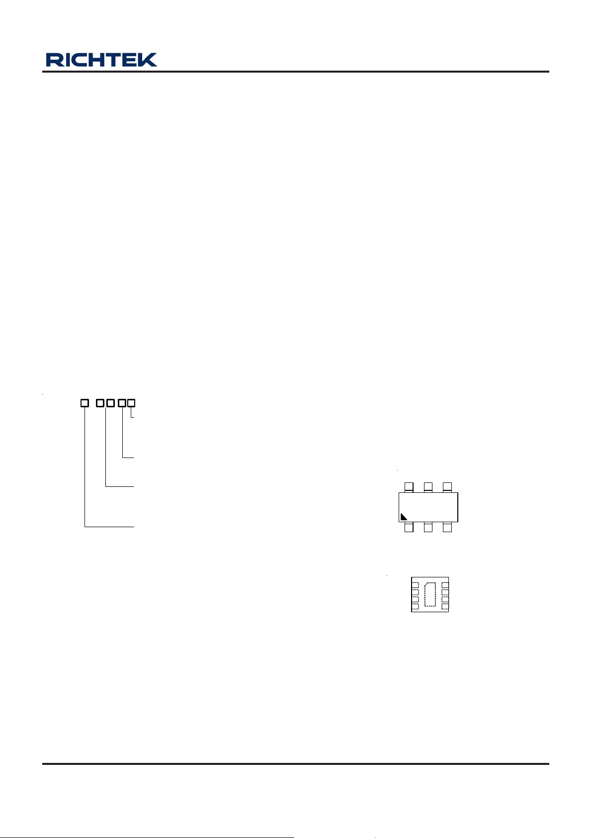
Pin Configurations
(TOP VIEW)
VINVOUT EN
4
56
23
LX GND FB
TSOT-23-6
1
GND
2
VIN
3
VOUT
4
EN
WDFN-8L 2x2
8
LX
7
NC
GND
6
FB
9
5
GND
Marking Information
For marking information, contact our sales re presentative
directly or through a Richtek distributor located in your
area.
DS9293-01 April 2011 www.richtek.com
1
RT9293
Typical Application Circuit
22µH to 47µH
L
D
V
OUT
V
IN
Chip Enable
C
2.2µF
Functional Pin Description
Pin No.
RT9293□GJ6 RT9293□GQW
1 8 LX Switching Pin.
2
1, 5,
9 (Exposed pad)
3 6 FB Feedback Pin, put a resistor to GND to setting the current.
4 4 EN Chip Enable (A ctive High).
5 3 VOUT Output Voltage Pin.
6 2 VIN Input Supply.
Pin Name Pin Function
GND
LX
VIN
IN
EN
GND
RT9293
VOUT
FB
C
OUT
1µF
10 WLEDs
R
SET
Ground Pin. The exposed pad must be soldered to a large
PCB and connected to GND for maximum power dis sipation.
-- 7 NC No Internal Connection.
Function Block Diagram
Internal
Compensation
Internal
Soft Start
EA
GM
-
VIN
UVLO
OTP
PWM
-
+
+
+
Compensation
LPF
V
REF
Slope
Enable
Logic
Logic Control,
Minimum On
Time
Shutdown
20ms
1µA
OVP
OCP
Current-
Sense
Driver
PWM
Oscillator
Reference
Voltage
Bias
Current
LX
VOUT
GND
FB
EN
DS9293-01 April 2011www.richtek.com
2
Absolute Maximum Ratings (Note 1)
RT9293
z Supply Input Voltage, V
z Switching Pin, LX---------------------------------------------------------------------------------------------------------- −0.3V to 50V
z VOUT------------------------------------------------------------------------------------------------------------------------- −0.3V to 46V
z Other Pins------------------------------------------------------------------------------------------------------------------- −0.3V to 6V
z Power Dissipation, P
------------------------------------------------------------------------------------------------ −0.3V to 6V
IN
@ T
D
= 25°C
A
TSOT-23-6------------------------------------------------------------------------------------------------------------------- 0.392W
WDFN−8L 2x2-------------------------------------------------------------------------------------------------------------- 0.606W
z Package Thermal Resistance (Note 2)
TSOT-23-6, θJA------------------------------------------------------------------------------------------------------------- 255°C/W
WDFN−8L 2x2, θJA-------------------------------------------------------------------------------------------------------- 165°C/W
WDFN−8L 2x2, θJC-------------------------------------------------------------------------------------------------------- 20°C/W
z Lead T e mperature (Soldering, 10 sec.)------------------------------------------------------------------------------- 26 0°C
z Junction T emperature----------------------------------------------------------------------------------------------------- 150°C
z Storage T emperature Range -------------------------------------------------------------------------------------------- −65°C to 150°C
Recommended Operating Conditions (Note 3)
z Junction T emperature Range-------------------------------------------------------------------------------------------- −40°C to 125°C
z Ambient T emperature Range--------------------------------------------------------------------------------------------
−40°C to 85°C
Electrical Characteristics
(V
= 3.7V, C
IN
Input Voltage VIN 2.5 -- 5.5 V
Under V oltage Lock Ou t V
UVLO Hyst er esis -- 0.1 -- V
Quiescent Current IQ FB = 1.5V, No Switching -- 400 600 μA
Supply Current IIN FB = 0V, Sw itc hi ng -- 1 2 mA
Shut down Current I
Line Re gulation VIN = 3 to 4.3V -- 1 -- %
Load Regulation 1mA to 20mA -- 1 -- %
Operation Frequency f
Maxi mu m Duty Cycle 90 9 2 -- %
Clo ck Rat e 0.1 -- 200 kHz
Feedback Reference
Voltage
= 2.2μF, C
IN
= 0.47μF, I
OUT
= 20mA, L = 22μH, TA = 25°C, unless otherwise specified)
OUT
Parameter Symbol Test Conditions Min Typ Max Unit
2 2.2 2.45 V
UVLO
VEN < 0.4V -- 1 4 μA
SHDN
0.75 1 1.25 MHz
OSC
RT9293A 94 104 114
RT9293B
V
REF
285 300 315
mV
On Res ist ance R
-- 0.7 1.2 Ω
DS(ON)
To be continued
DS9293-01 April 2011 www.richtek.com
3

RT9293
Parameter Symbol Test Conditions Min Typ Max Unit
EN Threshold
Voltage
E N S ink C u rre n t
Logic-High VIH 1.4 -- -Logic-Low V
-- -- 0.5
IL
I
IH
-- 1 --
μA
V
EN Hyster esi s -- 0.1 -- V
Over-V oltage
Threshold
Over-Current Threshold
OTP
OVP = 50V 42 46 50
V
RT9293B-20
OVP
I
OCP
T
OTP
16 17.5 20
1 1.2 -- A
-- 160 --
V
°C
OTP Hysteresis -- 30 -- °C
Shutdown Dela y
Note 1. Stresses listed as the above “Absolute Maximum Ratings” may cause permanent damage to the device. These are for
stress ratings. Functional operation of the device at these or any other conditions beyond those indicated in the
operational sections of the specifications is not implied. Exposure to absolute maximum rating conditions for extended
periods may remain possibility to affect device reliability.
Note 2. θ
Note 3. The device is not guaranteed to function outside its operating conditions.
is measured in the natural convection at TA = 25°C on a low effective single layer thermal conductivity test board of
JA
JEDEC 51-3 thermal measurement standard. The case point of θ
T
SHDN
-- 20 -- ms
is on the expose pad for the WDFN package.
JC
DS9293-01 April 2011www.richtek.com
4

Typical Operating Characteristics
)
)
RT9293
Efficiency vs. Output Current
100
90
80
70
60
50
40
Efficiency (%)
30
20
10
0
0 0.05 0.1 0.15 0.2 0.25 0.3
Output Current (A)
Output Voltage vs. Output Current
40
35
30
V
V
IN
V
OUT
= 4.5V
= 4V
IN
= 10V
Efficiency vs. Input Voltage
100
I
= 30mA
90
80
70
60
50
40
Efficiency (%)
30
20
10
0
2.533.544.555.5
I
LOAD
= 20mA
LOAD
I
LOAD
V
= 10mA
OUT
= 34V
Input Voltage ( V )
Quiescent Current vs. Input Voltage
500
450
400
25
20
Output Voltage (V)
15
V
= 3.7V, V
10
5 1525354555657585
IN
OUT
= 34V
Output Current (mA)
Frequency vs. Input Voltage
1100
1050
1000
950
900
Frequency ( kH z)
850
I
= 20mA
800
2.5 3 3.5 4 4.5 5 5.5
Input Voltage (V)
LED
350
300
Quiescent Curre nt (µA
250
200
2.5 3 3.5 4 4.5 5 5.5
Input Voltage (V )
Frequency vs. Temperature
1100
1050
1000
950
900
Frequency ( kHz
850
V
= 3.7V, I
800
-40 -25 -10 5 20 35 50 65 80 95 110 125
Temperature ( °C)
IN
V
LED
= 1.5V
FB
= 20mA
DS9293-01 April 2011 www.richtek.com
5
 Loading...