


Richtek R7735AGE, R7735AGN, R7735GGE, R7735GGN, R7735HGE Schematics
...
®
High Performance Enhanced Quadruple Mode PWM
Flyback Controller
R7735
General Description
R7735 series is the successor of R7732/3 and fully
compatible with most of SOT-23-6 / DIP-8 product so far
in the market. It has enhanced quadruple mode PWM
controller and owns excellent green power performance,
especially under light load and no load conditions. It
focuses on "easy to design" in different applications and
it will save both design effort and external components.
Besides the general features shown in the Features
section, R7735 covers wide protection options, such as
internal Over Load Protection (OLP) and Over Voltage
Protection (OVP) to eliminate the external protection
circuits. Moreover, it also features Secondary Rectifier
Short Protection (SRSP) and CS pin open protection. This
protection will make the PSU design for reliability and
safety easier.
R7735 is designed for power supply such as NB adaptor
which is a very cost effective and compact design. The
precise external OVP and Over Temperature Protection
(OTP) can be implemented by very simple circuit. The
start-up resistors can also be replaced by bleeding
resistors to save power loss and component count.
Features
zz
z No Load Input Power Under 100mW
zz
zz
z Accurate Over Load Protection
zz
zz
z UVLO 9V/14V
zz
zz
z Soft Start Function
zz
zz
z Current Mode Control
zz
zz
z Built-in Slope Compensation
zz
zz
z Internal Leading Edge Blanking
zz
zz
z PWM Quadruple Mode for Green-Mode
zz
zz
z Excellent Green Power Performance
zz
zz
z Cycle-by-Cycle Current Limit
zz
zz
z Internal Over Voltage Protection
zz
zz
z Secondary Rectifier Short Protection
zz
zz
z Opto-Coupler Short Protection
zz
zz
z Feedback Open-Loop Protection
zz
zz
z CS Pin Open Protection
zz
zz
z Built-in Jittering Frequency
zz
zz
z Built-in PRO Pin for External Arbitrary OVP/OTP
zz
zz
z Soft Driving for EMI Noise
zz
zz
z High Noise Immunity
zz
zz
z RoHS Compliant and Halogen Free
zz
Application
zz
z Switching AC/DC Adaptor
Ordering Information
R7735
(B)* (* : See Version Table)
Package Type
E : SOT-23-6
N : DIP-8 (R7735G Only)
Lead Plating System
zz
zz
z DVD Open Frame Power Supply
zz
zz
z Set-T op Box (STB)
zz
zz
z ATX Standby Power
zz
zz
z TV/Monitor Standby Power
zz
zz
z PC Peripherals
zz
zz
z NB Adaptor
zz
G : Green (Halogen Free and Pb Free)
R7735 Version (Refer to Version Table)
Note :
Richtek products are :
` RoHS compliant and compatible with the current
requirements of IPC/JEDEC J-STD-020.
` Suitable for use in SnPb or Pb-free soldering processes.
Copyright 2012 Richtek Technology Corporation. All rights reserved. is a registered trademark of Richtek Technology Corporation.
R7735-03 September 2012 www.richtek.com
©
Marking Information
For marking information, contact our sales representative
directly or through a Richtek distributor located in your
area.
1
R7735
Pin Configurations
(TOP VIEW)
GND
COMP
GATE
VDD CS
4
56
23
GND
SOT-23-6
COMP
PRO
GATE
23
DIP-8
R7735 Version Table
Version R7735G R7735R R7735L R7735A R7735H
Frequency 65kHz 65kHz 65kHz 65kHz 100kHz
OLP Delay Time 56ms 56ms 56ms 28ms 36ms
Internal OVP(27V) Auto Recovery Auto Recovery Latch Latch Auto Recovery
OLP & SRSP Auto Recovery Auto Recovery Auto Recovery Latc h Auto Recovery
PRO Pin High Latch Auto Recovery Latc h Latch Auto Recover y
PRO Pin Low Auto Recovery Latch Latch Latch Latch
* : V
R7735XGE : V
R7735HGE(B) : V
: Secondary Rectifier Short Protection (SRSP) triggered threshold.
SRSP_TH
= 1.7V, X = G/R/L/A
SRSP_TH
= 2.6V
SRSP_TH
NC
NCVDD
PRO
678
5
4
CS
Typical Application Circuit
AC Mains
(90V to 265V)
PRO
COMP
NTC
VDD
R7735
GND
GATE
CS
+
#
# : See Application Information
Vo+
+
Vo-
Copyright 2012 Richtek Technology Corporation. All rights reserved. is a registered trademark of Richtek Technology Corporation.
www.richtek.com
©
R7735-03 September 2012
2
Functional Pin Description
R7735
Pin No.
Pin Name Pin Function
SOT-23-6 DIP-8
1 8 GND Ground.
2 7 COMP
Voltage Feedback. By connecting an opto-coupler to close control loop
and achieve the regulation.
3 5 PRO For External Arbitrary OVP or OTP.
4 4 CS Primary Current Sense.
5 2 VDD Power Supply.
6 1 GATE Gate Drive Output to Drive the External MOSFET.
-- 3, 6 NC No Internal Connection.
Function Block Diagram
V
L_TH
PRO
I
BIAS
V
SRSP_TH
V
H_TH
+
-
+
-
Secondary Rectifier Short
& CS Open Protection
+
Brownout
Sensing
COMP Open
Sensing
OLP
Auto
Recovery
Latch
Auto
Recovery
Latch
POR
Shutdown
Logic
Counter
Oscillator
OVP
UVLO
+
-
+
-
Bias &
Bandgap
VDD
27V
9V/14V
-
+
PWM
Dmax
S
R
Quadruple Mode
Q
Soft Driver
V
COMP
V
BURL
V
BURH
V
DD
www.richtek.com
Constant
Power
COMP
CS
LEB
Copyright 2012 Richtek Technology Corporation. All rights reserved. is a registered trademark of Richtek Technology Corporation.
©
X3
SS
Slope
Ramp
Comparator
R7735-03 September 2012
GATE
GND
3
R7735
Absolute Maximum Ratings (Note 1)
z Supply Input Voltage, VDD ----------------------------------------------------------------------------------------------- −0.3V to 30V
z GATE Pin--------------------------------------------------------------------------------------------------------------------- −0.3V to 16.5V
z PRO, COMP, CS Pin ------------------------------------------------------------------------------------------------------ −0.3V to 6.5V
z I
------------------------------------------------------------------------------------------------------------------------------ 10mA
DD
z Power Dissipation, P
SOT-23-6 -------------------------------------------------------------------------------------------------------------------- 0.400W
DIP-8-------------------------------------------------------------------------------------------------------------------------- 0.714W
z Package Thermal Resistance (Note 2)
SOT-23-6, θJA--------------------------------------------------------------------------------------------------------------- 250°C/W
DIP-8, θJA-------------------------------------------------------------------------------------------------------------------- 140°C/W
z Junction Temperature ------------------------------------------------------------------------------------------------------ 150°C
z Lead Temperature (Soldering, 10 sec.) -------------------------------------------------------------------------------- 260°C
z Storage Temperature Range --------------------------------------------------------------------------------------------- −65°C to 150°C
z ESD Susceptibility (Note 3)
HBM (Human Body Model)----------------------------------------------------------------------------------------------- 3kV
MM (Machine Model) ------------------------------------------------------------------------------------------------------ 250V
@ TA = 25°C
D
Recommended Operating Conditions (Note 4)
z Supply Input Voltage, VDD ----------------------------------------------------------------------------------------------- 12V to 25V
z Junction Temperature Range --------------------------------------------------------------------------------------------- −40°C to 125°C
z Ambient Temperature Range --------------------------------------------------------------------------------------------- −40°C to 85°C
Electrical Characteristics
(V
= 15V, T
DD
VDD Section
VDD Over Voltage Protection Level V
VDD Zener Clamp VZ 29 -- -- V
On Threshold Voltage V
Off Threshold Voltage V
VDD Holdup Mode Entry Point V
VDD Holdup Mode Ending Point V
Latch-off Voltage VLH 4.5 5.5 6.5 V
Latched Reset Voltage V
Start-up Current I
Oper ating Supply Current I
= 25°C, unless otherwise specified)
A
Parameter Symbol Test Conditions Min Typ Max Unit
26 27 28 V
OVP
13 14 15 V
TH_ON
TH_OFF
DD_LOW
DD_HIGH
LH_RST
DD_ST
DD_OP
8.5 9 9.5 V
V
V
< 1.6V 9.5 10 10.5 V
COMP
< 1.6V 10 10.5 11 V
COMP
4 5 6 V
V
DD
= −40ºC to 100ºC (Note 5)
T
A
V
DD
GATE pin open
= V
TH_ON –
= 15V, V
COMP
0.2V,
= 2.5V,
1 5 10 μA
0.55 0.9 1.6 mA
Latch-off Operating Current I
TA= −40ºC to 100ºC (Note 5) 2 -- 8 μA
DD_LH
Copyright 2012 Richtek Technology Corporation. All rights reserved. is a registered trademark of Richtek Technology Corporation.
www.richtek.com
4
©
R7735-03 September 2012
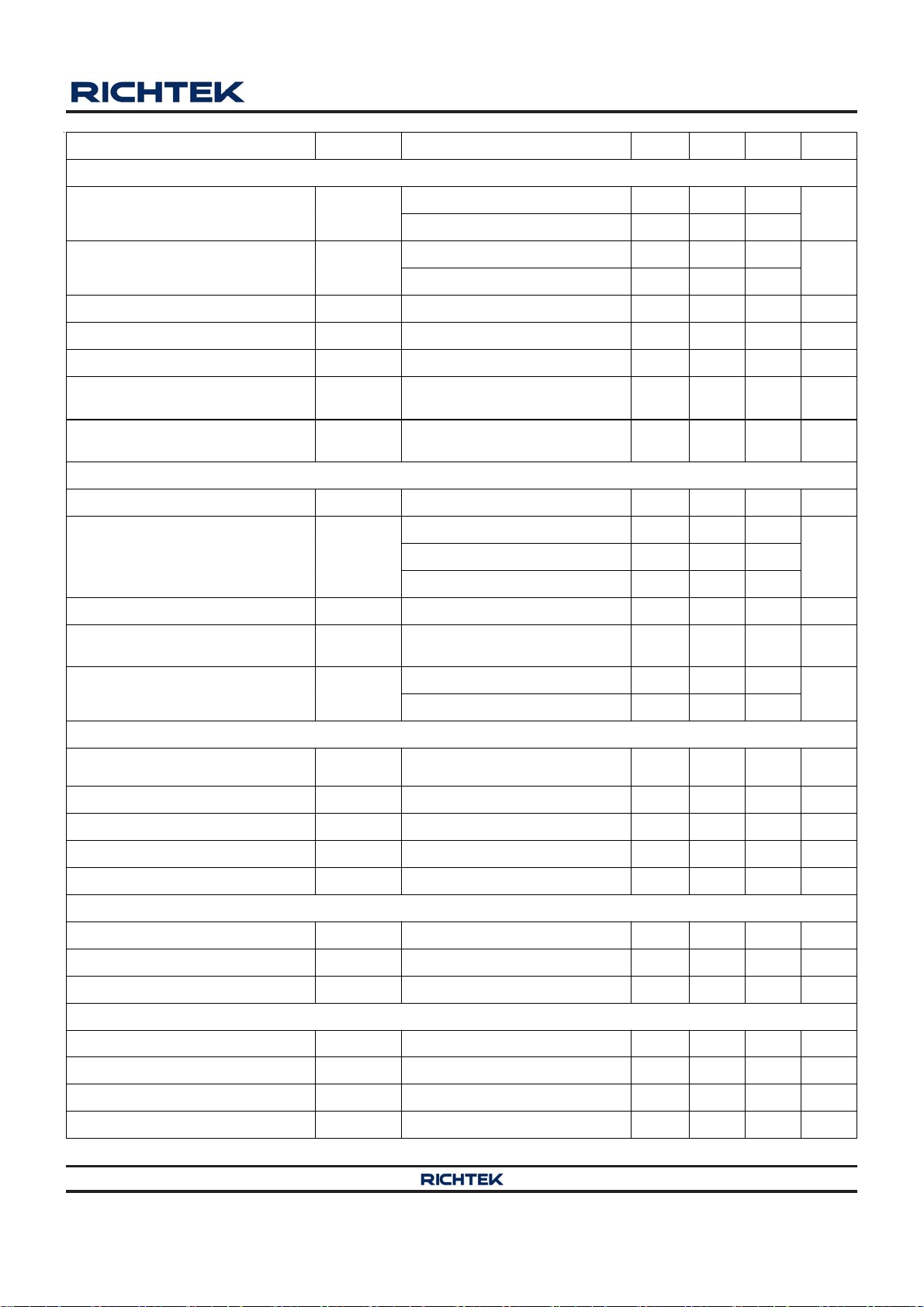
Parameter Symbol Test Conditions Min Typ Max Unit
Oscillator Section
R7735
Normal PWM Frequency f
Frequency Reduction Mode
Minimum Frequency
Maximum Duty Cycle DCY
OSC
f
FR_MIN
R7735H 92 100 108
R7735G/R/L/A 18 22 -R7735H -- 25 --
70 75 80 %
MAX
kHz
kHz
PWM Frequency Jitter Range Δf -- ±6 -- %
R7735G/R/L/A 60 65 70
PWM Frequency Jitter Period T
Frequency Variation Versus
V
Deviation
DD
Frequency Variation Versus
Temperature Deviation
For 65kHz -- 4 -- ms
JIT
V
f
DV
f
DT
= 12V to 25V -- -- 2 %
DD
= −30°C to 105°C
T
A
(Note 5)
-- -- 5 %
COMP In put Section
Open-Loop Voltage V
COMP_OP
COMP pin Open 5.5 5.75 6 V
R7735G/R/L 45 56 65
COMP Open-Loop Protection
Delay Time
T
OLP
R7735A 22 28 34
ms
R7735H 30 36 42
Short Circuit Current I
Frequency Reduction Mode Entry
Voltage
Frequency Reduction Mode
Ending Voltage
V
ZERO
V
V
2.85 3 3.15 V
FR_ET
FR_ED
= 0V 0.15 0.29 0.45 mA
COMP
R7735G/R/L/A 2.75 2.9 3.05
V
R7735H 2.65 2.8 2.95
Current Sense Section
Initial Peak Current Limitation
Offset
Maximum Clamping Current Limit V
Leading Edge Blanking Time t
V
0.68 0.7 0.72 V
CS_TH
CS(MAX)
LEB
1.05 1.1 1.15 V
(Note 6) 150 250 350 ns
Internal Propagation Delay Time tPD (Note 6) -- 100 -- ns
Minimum On Time t
ON(MIN)
250 350 450 ns
GATE Section
Rising Time tR V
Falling Time tF V
GATE Output Clamping Voltage V
VDD= 25V 12.1 14 15.9 V
CLAMP
= 15V, CL= 1nF 60 125 140 ns
DD
= 15V, CL= 1nF 25 40 65 ns
DD
PRO Interface Section
Pull Low Threshold V
Pull High Threshold V
Internal Bias Current I
Pull High Sinking Current I
Copyright 2012 Richtek Technology Corporation. All rights reserved. is a registered trademark of Richtek Technology Corporation.
R7735-03 September 2012
©
0.47 0.5 0.53 V
L_TH
3.5 3.8 4.1 V
H_TH
90 100 110 μA
BIAS
(Note 7) 0.7 -- 1.4 mA
SINK
www.richtek.com
5
R7735
Note 1. Stresses beyond those listed “Absolute Maximum Ratings” may cause permanent damage to the device. These are
stress ratings only, and functional operation of the device at these or any other conditions beyond those indicated in the
operational sections of the specifications is not implied. Exposure to absolute maximum rating conditions may affect
device reliability.
Note 2. θ
is measured at T
JA
Note 3. Devices are ESD sensitive. Handling precaution is recommended.
Note 4. The device is not guaranteed to function outside its operating conditions.
Note 5. Guaranteed by design.
Note 6. Leading edge blanking time and internal propagation delay time are guaranteed by design.
Note 7. The sourcing current of PRO pin must be limited below 5mA. Otherwise it may cause permanent damage to the
device.
= 25°C on a low effective thermal conductivity single-layer test board per JEDEC 51-3.
A
Copyright 2012 Richtek Technology Corporation. All rights reserved. is a registered trademark of Richtek Technology Corporation.
www.richtek.com
©
R7735-03 September 2012
6
 Loading...