

®
RT9724
100m
ΩΩ
Ω, 2A Slew Rate Controlled Load Switch
ΩΩ
General Description
The RT9724 is a cost-effective, low-voltage, single
N-MOSFET high-side Power Switch IC. Low switch-on
resistance (typ. 100mΩ) and low supply current (typ. 50uA)
are realized in this IC. The RT9724 integrates an over-
current protection circuit, a short fold back circuit, a
thermal shutdown circuit and an under-voltage lockout
circuit for overall protection. Besides, a slew rate
controlled function is embedded for turn-on rising time
control. The RT9724 is available in SOT-23-5 and WDFN-
8L 2x2 package.
Ordering Information
RT9724
Package Type
B : SOT-23-5
QW : WDFN-8L 2x2 (W-Type)
Lead Plating System
G : Green (Halogen Free and Pb Free)
Note :
Richtek products are :
` RoHS compliant and compatible with the current require-
ments of IPC/JEDEC J-STD-020.
` Suitable for use in SnPb or Pb-free soldering processes.
Features
zz
z
zz
zz
z Operating Range : 2.7V to 5.5V
zz
zz
z Reverse Blocking Current
zz
zz
z Under Voltage Lockout
zz
zz
z Thermal Protection with Foldback
zz
zz
z Over Current Protection
zz
zz
z Short Circuit Protection
zz
zz
z Slew Rate Limited Turn-On Time 3ms (5V)
zz
zz
z RoHS Compliant and Halogen Free
zz
ΩΩ
100m
Ω (typ.) N-MOSFET Switch
ΩΩ
Applications
z Cellular Phones
z Digital still Camera
z Hot swap Supplies
z Notebook Computers
z Personal Communication Devices
z Personal Digital Assistants
Pin Configurations
(TOP VIEW)
VIN
5
VIN
4
23
Marking Information
RT9724GB
1Y= : Product Code
1Y=DNN
DNN : Date Code
RT9724GQW
GV : Product Code
GVW
Copyright 2012 Richtek Technology Corporation. All rights reserved. is a registered trademark of Richtek Technology Corporation.
©
W : Date Code
DS9724-02 July 2012 www.richtek.com
EN GND VOUT
SOT-23-5
1
NC
2
VOUT
3
4
GND
WDFN-8L 2x2
GND
9
8
VIN
7
VIN
6
VINEN
5
VIN
1

RT9724
Typical Application Circuit
2.7V to 5.5V
Chip Enable
C
IN
1µF
EN
VOUTVIN
RT9724
GND
Functional Pin Description
Pin No.
SOT-23-5 WDFN-8L 2x2
1 3 EN Chip Enable (Active High).
2
9 (Exposed Pad)
4,
3 2 VOUT Power-Switch Output.
4, 5 5, 6, 7, 8 VIN Power Input Voltage.
-- 1 NC No Internal Connection.
Pi n Na me Pi n Functi o n
GND
Ground. The exposed pad must be soldered to a large PCB and
connected to GND for maximum power dissipation.
Function Block Diagram
C
OUT
0.1µF
Load
EN
Bias
Oscillator
UVLO
Charge
Pump
Thermal
Protection
Gate
Control
Current
Limiting
Output Voltage
Detection
Auto Discharge
VIN
VOUT
GND
Copyright 2012 Richtek Technology Corporation. All rights reserved. is a registered trademark of Richtek Technology Corporation.
©
DS9724-02 July 2012www.richtek.com
2
RT9724
Absolute Maximum Ratings (Note 1)
z Supply Voltage, VIN ------------------------------------------------------------------------------------------------------ 6V
z Enable Input Voltage, EN ------------------------------------------------------------------------------------------------ −0.3V to 6V
z Power Dissipation, P
D
SOT-23-5 -------------------------------------------------------------------------------------------------------------------- 0.458W
WDFN-8L 2x2 -------------------------------------------------------------------------------------------------------------- 0.833W
z Package Thermal Resistance (Note 2)
SOT-23-5, θJA-------------------------------------------------------------------------------------------------------------- 218.1°C/W
WDFN-8L 2x2, θJA-------------------------------------------------------------------------------------------------------- 120°C/W
z Junction Temperature ----------------------------------------------------------------------------------------------------- 150°C
z Lead Temperature (Soldering, 10 sec.) ------------------------------------------------------------------------------- 260°C
z ESD Susceptibility (Note 3)
HBM (Human Body Model)---------------------------------------------------------------------------------------------- 4kV
Recommended Operating Conditions (Note 4)
z Supply Voltage, VIN ------------------------------------------------------------------------------------------------------ 2.7V to 5.5V
z Enable Input Voltage, EN ------------------------------------------------------------------------------------------------ 0V to 5.5V
z Junction Temperature Range -------------------------------------------------------------------------------------------- −40°C to 100°C
z Ambient Temperature Range --------------------------------------------------------------------------------------------
@ T
= 25°C
A
−40°C to 85°C
Electrical Characteristics
(VIN = 5V, CIN = 1μF, C
Parameter Symbol Test Conditions Min Typ Max Unit
Operation Voltage VIN 2.7 -- 5 V
Under Voltage Lookout V
Under Voltage Lockout
Hysteresis
Quiescent Current IQ EN = High -- 50 70 μA
Off Supply Current I
Off Switch Current I
On-Resistance R
Curr ent Limiting I
Short Circuit Current I
Thermal shutdown Threshold TSD
Hysteresis -- 20 -- °C
EN Threshold
Voltage
Enable Input Leakage IEN V
= 0.1μF, T
OUT
Logic-Low VIL V
Logic-High V
= 25°C, unless otherwise specified)
A
VIN Falling 1.3 1.7 2.1 V
UVLO
ΔV
SHDN
LEAKA GE
LIM
SC_FB
-- 50 -- mV
UVLO
EN = Low, V
EN = Low, V
VIN = 3.3V, I
DS(ON)
V
V
IH
= 3.3V, V
IN
V
= 0V, Measured Prior to
OUT
Thermal Shutdown
V
> 1V -- 130 -- °C
OUT
V
= 0V -- 100 -- °C
OUT
= 2.7V to 5.5V -- -- 0.8 V
IN
= 2.7V to 5.5V 2 -- -- V
IN
= 5.5V -- -- 1 μA
EN
= Open -- -- 1 μA
OUT
= 0 -- -- 1 μA
OUT
= 1.3 A -- 100 120 mΩ
OUT
= 2.3V 1.5 2 2.5 A
OUT
0.4 0.8 1.5 A
Copyright 2012 Richtek Technology Corporation. All rights reserved. is a registered trademark of Richtek Technology Corporation.
DS9724-02 July 2012 www.richtek.com
©
3
RT9724
Parameter Symbol Test Conditions Min Typ Max Unit
Output Turn-On Delay Time T
Output Turn-On Rise Time TON V
Output Turn-Off Delay Time T
Output Pull-Down Resistance
During OFF
Note 1. Stresses beyond those listed “Absolute Maximum Ratings” may cause permanent damage to the device. These are
stress ratings only, and functional operation of the device at these or any other conditions beyond those indicated in
the operational sections of the specifications is not implied. Exposure to absolute maximum rating conditions may
affect device reliability.
Note 2. θ
Note 3. Devices are ESD sensitive. Handling precaution is recommended.
Note 4. The device is not guaranteed to function outside its operating conditions.
is measured at T
JA
= 25°C on a high effective thermal conductivity four-layer test board per JEDEC 51-7.
A
VIN = 5V, R
D_ON
VIN = 5V, R
D_OFF
R
DI SCHA RGE
= 10Ω -- 60 100 μs
LOAD
= 5V, R
IN
= 10Ω 1 3 -- ms
LOAD
= 10Ω -- 4 10 μs
LOAD
EN = Low -- 150 -- Ω
Copyright 2012 Richtek Technology Corporation. All rights reserved. is a registered trademark of Richtek Technology Corporation.
4
©
DS9724-02 July 2012www.richtek.com
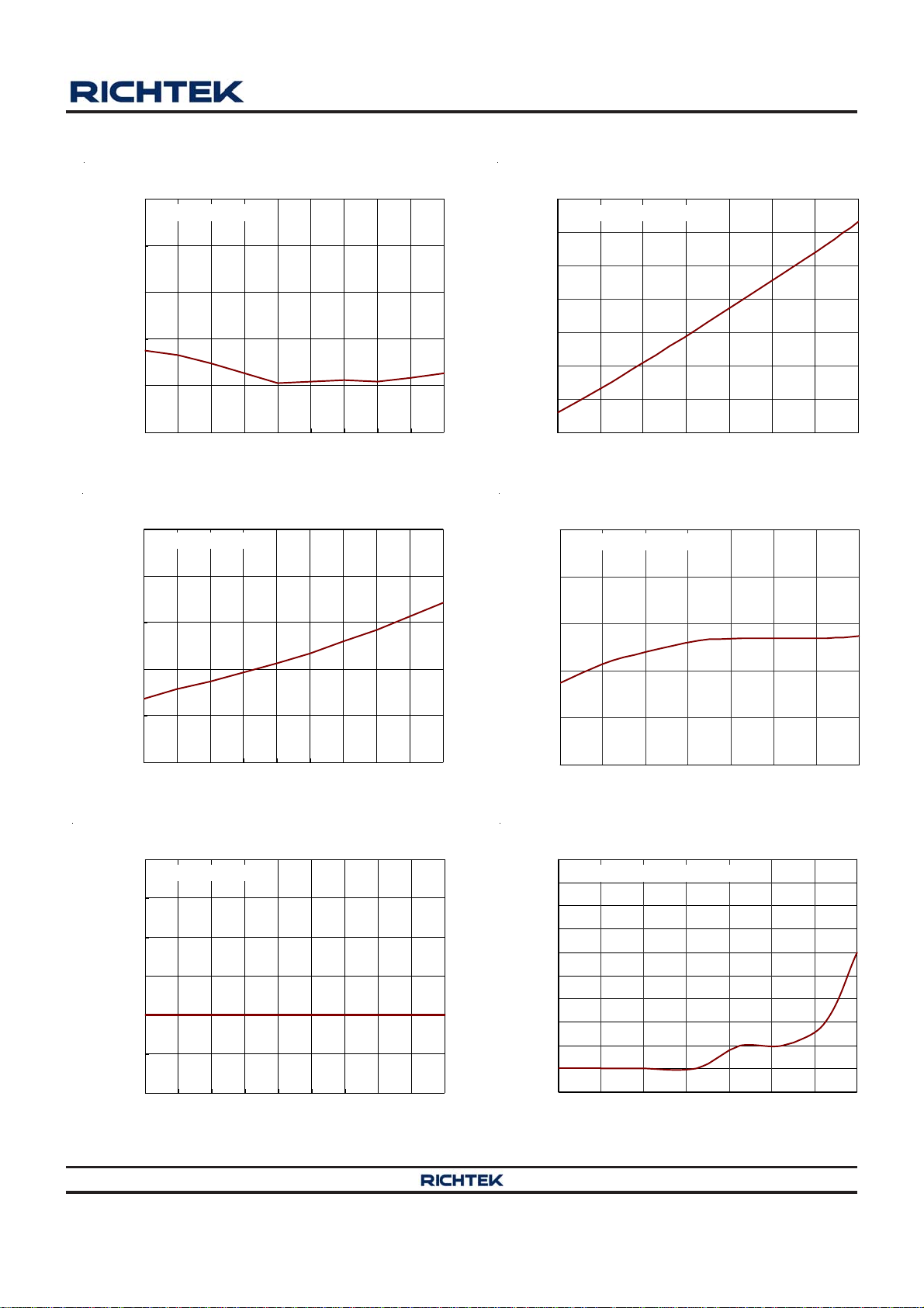
Typical Operating Characteristics
)
)
RT9724
On Resistance vs. Input Voltage
115
EN = 5V, I
114
113
112
On Resistance (mΩ)
111
110
2.7 3.1 3.4 3.7 4 4.3 4.6 4.9 5.2 5.5
OUT
= 1.5A
Input Voltage (V)
Quiescent Current vs. Input Voltage
30
VEN = 5V, No Load
27
24
On Resistance vs. Temperature
150
VIN = VEN = 5V, I
140
130
120
110
100
On Resistance (mΩ)
90
80
-40 -20 0 20 40 60 80 100
OUT
= 1.5A
Temperature (°C)
Quiescent Current vs. Temperature
30
VIN = VEN = 5.5V, No Load
28
26
21
Quiescent Current (µA
18
15
2.7 3.1 3.4 3.7 4 4.3 4.6 4.9 5.2 5.5
Input Voltage (V)
Shutdown Current vs. Input Voltage
0.30
VEN = 0V,No Load
0.25
0.20
0.15
0.10
Shutdown Current (µA) 1
0.05
0.00
2.7 3.1 3.4 3.7 4 4.3 4.6 4.9 5.2 5.5
Input Voltage (V)
Copyright 2012 Richtek Technology Corporation. All rights reserved. is a registered trademark of Richtek Technology Corporation.
©
24
Quiescent Current (µA
22
20
-40 -20 0 20 40 60 80 100
Temperature (°C)
Shutdown Current vs. Tem perature
1
VIN = 5.5V, VEN = 0V, No Load
0.9
0.8
0.7
0.6
0.5
0.4
0.3
0.2
Shutdown Current (µA) 1
0.1
0
-40-200 20406080100
Temperature (°C)
DS9724-02 July 2012 www.richtek.com
5

RT9724
Output Voltage vs. Output Current
6
VIN = 5.5V
5
4
VIN = 3.3V
3
2
Output Voltage (V)
1
0
0.2 0.4 0.6 0.8 1.0 1.2 1.4 1.6 1.8 2.0 2.2
Output Current (A)
Current Limit vs. Input Voltage
2
1.9
1.8
VEN = 5V
UVLO Threshold vs. Temperature
2.1
1.9
Rising
1.7
1.5
UVLO Threshold (V)
1.3
1.1
-40-20 0 20406080100
Falling
VEN = 5V
Temperature (°C)
Short Current vs. Input Voltage
1.2
1.1
1
1.7
Current Limit (A)
1.6
1.5
2.7 3.1 3.4 3.7 4 4.3 4.6 4.9 5.2 5.5
VEN = 5V
Input Voltage (V)
Current Limit vs. Temperature
2
1.9
1.8
1.7
Current Limit (A)
1.6
1.5
-40 -20 0 20 40 60 80 100
Temperature (°C)
VEN = 5V
0.9
Short Current (A)
0.8
0.7
2.7 3.1 3.4 3.7 4 4.3 4.6 4.9 5.2 5.5
VEN = 5V
Input Voltage (V)
Short Current vs . Te m p e rature
1.2
1.1
1
0.9
Short Current (A)
0.8
0.7
-40-20020406080100
Temperature (°C)
VIN = VEN = 5V
Copyright 2012 Richtek Technology Corporation. All rights reserved. is a registered trademark of Richtek Technology Corporation.
©
DS9724-02 July 2012www.richtek.com
6

RT9724
)
Turn-On Rising Time vs. Input Voltage
4
3.7
3.4
3.1
2.8
Turn-On Rising Time (ms
VEN = 5V, R
2.5
2.7 3.1 3.4 3.7 4 4.3 4.6 5 5.2 5.5
LOAD
= 10Ω
Input Voltage (V)
Turn-Off Delay Time v s . Input Voltage
1.2
1
0.8
0.6
Turn On Rising Time v s. Tem perature
5
4.6
4.2
3.8
3.4
Turn On Rising Time (ms)
VIN = VEN = 5V, R
3
-40 -20 0 20 40 60 80 100
LOAD
= 10Ω
Temperature (°C)
Turn Off Delay Tim e vs. Temperature
0.6
0.5
0.4
0.4
Turn-Off Delay Time (µs)
0.2
V
IN
(2V/Div)
VEN = 5V, R
2.7 3.1 3.4 3.7 4 4.3 4.6 5 5.2 5.5
LOAD
= 10Ω
Input Voltage (V)
Power On from V
IN
0.3
Turn Off Delay Time (µs)
0.2
V
OUT
(2V/Div)
V
EN
VEN = 5V, R
-40-200 20406080100
LOAD
= 10Ω
Temperature (°C)
Power On from EN
(5V/Div)
V
OUT
(2V/Div)
VIN = VEN = 5V, No Load
Time (5ms/Div)
I
OUT
(1V/Div)
VIN = VEN = 5.5V, R
Time (2.5ms/Div)
LOAD
= 3Ω
Copyright 2012 Richtek Technology Corporation. All rights reserved. is a registered trademark of Richtek Technology Corporation.
©
DS9724-02 July 2012 www.richtek.com
7

RT9724
Applications Information
The RT9724 is a single N-MOSFET high-side power
switches with enable input, optimized for self-powered and
bus-powered Universal Serial Bus (USB) applications. The
RT9724 is equipped with a charge pump circuitry to drive
the internal N-MOSFET switch; the switch's low R
DS(ON)
100mΩ, meets USB voltage drop requirements.
Input and Output
VIN (input) is the power source connection to the internal
circuitry and the drain of the MOSFET. V
(output) is
OUT
the source of the MOSFET. In a typical application, current
flows through the switch from VIN to V
If V
is greater than VIN, current will flow from V
OUT
V
since the MOSFET is bidirectional when on.
IN
toward the load.
OUT
OUT
to
Unlike a normal MOSFET, there is no parasitic body diode
between drain and source of the MOSFET, the RT9724
prevents reverse current flow if V
is externally forced
OUT
to a higher voltage than VIN when the chip is disabled
(V
< 0.8V).
EN
D
D
G
S
G
S
Normal MOSFET RT9724
Chip Enable Input
The switch will be disabled when the EN pin is in a logic
low condition. During this condition, the internal circuitry
and MOSFET will be turned off, reducing the supply current
to 0.1μA typical. Floating the EN may cause unpredictable
operation. EN should not be allowed to go negative with
respect to GND. The EN pin may be directly tied to VIN to
keep the part on.
Soft Start for Hot Plug-In Applications
In order to eliminate the upstream voltage droop caused
by the large inrush current during hot-plug events, the
“soft-start” feature effectively isolates the power source
from extremely large capacitive loads, satisfying the USB
voltage droop requirements.
Under Voltage Lockout
Under Voltage Lockout (UVLO) prevents the MOSFET
switch from turning on until the input voltage exceeds
approximately 1.75V. If input voltage drops below
approximately 1.7V, UVLO turns off the MOSFET switch.
,
Under-voltage detection functions only when the switch
is enabled.
Current Limiting and Short-Circuit Protection
The current limit circuitry prevents damage to the MOSFET
switch and the hub downstream port but can deliver load
current up to the current limit threshold of typically 2A.
When a heavy load or short circuit is applied to an enabled
switch, a large transient current may flow until the current
limit circuitry responds. Once this current limit threshold
is exceeded, the device enters constant current mode
until the thermal shutdown occurs or the fault is removed.
Universal Serial Bus (USB) & Power Distribution
The goal of USB is to enable device from different vendors
to interoperate in an open architecture. USB features
include ease of use for the end user, a wide range of
workloads and applications, robustness, synergy with the
PC industry, and low-cost implementation. Benefits
include self-identifying peripherals, dynamically attachable
and reconfigurable peripherals, multiple connections
(support for concurrent operation of many devices), support
for as many as 127 physical devices, and compatibility
with PC Plug-and-Play architecture.
The Universal Serial Bus connects USB devices with a
USB host: each USB system has one USB host. USB
devices are classified either as hubs, which provide
additional attachment points to the USB, or as functions,
which provide capabilities to the system (for example, a
digital joystick). Hub devices are then classified as either
Bus-Power Hubs or Self-Powered Hubs.
A Bus-Powered Hub draws all of the power to any internal
functions and downstream ports from the USB connector
power pins. The hub may draw up to 500mA from the
upstream device. External ports in a Bus-Powered Hub
can supply up to 100mA per port, with a maximum of four
external ports.
Copyright 2012 Richtek Technology Corporation. All rights reserved. is a registered trademark of Richtek Technology Corporation.
8
©
DS9724-02 July 2012www.richtek.com

RT9724
Self-Powered Hub power for the internal functions and
downstream ports does not come from the USB, although
the USB interface may draw up to 100mA from its
upstream connection, to allow the interface to function
when the remainder of the hub is powered down. The hub
must be able to supply up to 500mA on all of its external
downstream ports. Please refer to Universal Serial
Specification Revision 2.0 for more details on designing
compliant USB hub and host systems.
Over current protection devices such as fuses and PTC
resistors (also called polyfuse or polyswitch) have slow
trip times, high on-resistance, and lack the necessary
circuitry for USB-required fault reporting.
The faster trip time of the RT9724 power distribution allows
designers to design hubs that can operate through faults.
The RT9724 provides low on-resistance and internal fault-
reporting circuitry to meet voltage regulation and fault
notification requirements.
Because the devices are also power switches, the designer
of self-powered hubs has the flexibility to turn off power to
output ports. Unlike a normal MOSFET, the devices have
controlled rise and fall times to provide the needed inrush
current limiting required for the bus-powered hub power
switch.
Supply Filter/Bypass Ca pa citor
A 1uF low-ESR ceramic capacitor from V
to GND, located
IN
at the device is strongly recommended to prevent the input
voltage drooping during hot-plug events. However, higher
capacitor values will further reduce the voltage droop on
the input. Furthermore, without the bypass capacitor, an
output short may cause sufficient ringing on the input (from
source lead inductance) to destroy the internal control
circuitry. The input transient must not exceed 6V of the
absolute maximum supply voltage even for a short duration.
Output Filter Capacitor
A low-ESR 150uF aluminum electrolytic or tantalum
between V
the 330mV maximum droop requirement in the hub V
and GND is strongly recommended to meet
OUT
BUS
(Per USB 2.0, output ports must have a minimum 120μF
of low-ESR bulk capacitance per hub). Standard bypass
methods should be used to minimize inductance and
resistance between the bypass capacitor and the
downstream connector to reduce EMI and decouple voltage
droop caused when downstream cables are hot-insertion
transients. Ferrite beads in series with V
, the ground
BUS
line and the 0.1μF bypass capacitors at the power
connector pins are recommended for EMI and ESD
protection. The bypass capacitor itself should have a low
dissipation factor to allow decoupling at higher frequencies.
Voltage Drop
The USB specification states a minimum port-output
voltage in two locations on the bus, 4.75V out of a Self-
Powered Hub port and 4.4V out of a Bus-Powered Hub
port. As with the Self-Powered Hub, all resistive voltage
drops for the Bus-Powered Hub must be accounted for to
guarantee voltage regulation (see Figure 7-47 of Universal
Serial Specification Revision 2.0 ).
The following calculation determines V
ple ports (N
using one switch per port, N
V
OUT (MIN)
= 4.75V − [ II x ( 4 x R
(0.1A x N
) ganged together through one switch (if
PORTS
is equal to 1) :
PORTS
+ 2 x R
CONN
PORTS
x R
SWITCH
) − V
OUT (MIN)
CABLE
PCB
for multi-
) ] −
Where
R
= Resistance of connector contacts
CONN
(two contacts per connector)
R
= Resistance of upstream cable wires
CABLE
(one 5V and one GND)
R
= Resistance of power switch
SWITCH
(90mΩ typical for RT9715)
V
= PCB voltage drop
PCB
The USB specification defines the maximum resistance
per contact (R
) of the USB connector to be 30mΩ
CONN
and the drop across the PCB and switch to be 100mV.
This basically leaves two variables in the equation: the
resistance of the switch and the resistance of the cable.
If the hub consumes the maximum current (II) of 500mA,
the maximum resistance of the cable is 90mΩ.
Copyright 2012 Richtek Technology Corporation. All rights reserved. is a registered trademark of Richtek Technology Corporation.
DS9724-02 July 2012 www.richtek.com
©
9

RT9724
)
The resistance of the switch is defined as follows :
R
= (200mV − V
= { 4.75V − 4.4V − [ 0.5A x ( 4 x 30mΩ + 2 x
SWITCH
90mΩ) ] − V
}÷( 0.1A x N
PCB
)÷( 0.1A x N
PCB
PORTS
PORTS
)
)
If the voltage drop across the PCB is limited to 100mV,
the maximum resistance for the switch is 250mΩ for four
ports ganged together. The RT9724, with its maximum
100mΩ on-resistance over temperature, can fit the demand
of this requirement.
Thermal Shutdown
Thermal protection limits the power dissipation in the
RT9724. When the operation junction temperature
exceeds 130°C, the OTP circuit starts the thermal
shutdown function and turns the pass element off. The
pass element turn on again after the junction temperature
cools to 80°C. The RT9724 lowers its OTP trip level from
130°C to 100°C when output short circuit occurs (V
OUT
<
1V) as shown in Figure 1.
V
Short to GND
OUT
1V
V
OUT
Thermal Considerations
The maximum power dissipation depends on the thermal
resistance of IC package, PCB layout, the rate of
surroundings airflow and temperature difference between
junction to ambient. The maximum power dissipation can
be calculated by following formula :
P
where T
the ambient temperature, and θ
D(MAX)
= (T
J(MAX)
− TA) / θ
J(MAX)
JA
is the maximum junction temperature, T
is the junction to ambient
JA
A
thermal resistance.
For recommended operating conditions specification, the
maximum junction temperature is 125°C. The junction to
ambient thermal resistance θJA is layout dependent. For
SOT-23-5 package, the thermal resistance θJA is
218.1°C/W on the standard JEDEC 51-7 four layers
thermal test board. For WDFN-8L 2x2 package, the
thermal resistance θJA is 120°C/W on the standard JEDEC
51-7 four layers thermal test board. The maximum power
dissipation at TA = 25°C can be calculated by following
formula :
P
= (125°C − 25°C) / (218.1°C/W) = 0.458W for
D(MAX)
SOT-23-5 package
P
= (125°C − 25°C) / (120°C/W) = 0.833W for
D(MAX)
WDFN-8L 2x2 package
is
I
OUT
Thermal
Shutdown
°
130 C
110 C
OTP Trip Point
IC Temperature
°
100 C
80 C
°
°
Figure 1. Short Circuit Thermal Folded Back Protection
when Output Short Circuit Occurs (Patent)
The maximum power dissipation depends on operating
ambient temperature for fixed T
and thermal
J(MAX)
resistance θJA. The Figure 2 of derating curves allows the
designer to see the effect of rising ambient temperature
on the maximum power allowed.
1.0
0.9
0.8
0.7
0.6
SOT-23-5
0.5
0.4
0.3
0.2
0.1
Maximum Power Dissipation (W
0.0
0255075100125
WDFN-8L 2x2
Single Layer PCB
Ambient Temperature (°C)
Figure 2. Derating Curve of Maximum Power Dissipation
Copyright 2012 Richtek Technology Corporation. All rights reserved. is a registered trademark of Richtek Technology Corporation.
10
©
DS9724-02 July 2012www.richtek.com

Layout Consideration
For best performance of the RT9724.The following
guidelines must be followed :
` Input and Output capacitors should be placed close to
the IC and connected to ground plane to reduce noise
coupling.
` The GND shoule be connected to a strong ground plane
for heat sink.
` Keep the main current traces as possible as short and
wide.
The main current trace should be
as possible as short and wide.
VIN VIN
C
5
4
23
IN
RT9724
EN GND VOUT
C
OUT
The input and output capacitor should be
placed as close as possible to the IC.
Figure 3. PCB Layout Guide for SOT-23-5 Package
The input and output capacitor should be
placed as close as possible to the IC.
8
VIN
D
7
VIN
N
G
6
VIN
9
5
VIN
C
IN
C
OUT
NC
VOUT
EN
GND
1
2
3
4
The main current trace should be
as possible as short and wide.
Figure 4. PCB Layout for WDFN Package
Copyright 2012 Richtek Technology Corporation. All rights reserved. is a registered trademark of Richtek Technology Corporation.
©
DS9724-02 July 2012 www.richtek.com
11

RT9724
Outline Dimension
H
D
L
C
b
A
e
Dimensions In Millimeters Dimensions In Inches
Symbol
Min Max Min Max
A 0.889 1.295 0.035 0.051
A1 0.000 0.152 0.000 0.006
B 1.397 1.803 0.055 0.071
b 0.356 0.559 0.014 0.022
C 2.591 2.997 0.102 0.118
D 2.692 3.099 0.106 0.122
B
A1
e 0.838 1.041 0.033 0.041
H 0.080 0.254 0.003 0.010
L 0.300 0.610 0.012 0.024
SOT-23-5 Surface Mount Package
Copyright 2012 Richtek Technology Corporation. All rights reserved. is a registered trademark of Richtek Technology Corporation.
12
©
DS9724-02 July 2012www.richtek.com

RT9724
D
E
A
A3
A1
D2
L
E2
SEE DETAIL A
1
e
b
2
1
DETAIL A
1
2
Pin #1 ID and Tie Bar Mark Options
Note : The configuration of the Pin #1 identifier is optional,
but must be located within the zone indicated.
Dimensions In Millimeters Dimensions In Inches
Symbol
Min Max Min Max
A 0.700 0.800 0.028 0.031
A1 0.000 0.050 0.000 0.002
A3 0.175 0.250 0.007 0.010
b 0.200 0.300 0.008 0.012
D 1.950 2.050 0.077 0.081
D2 1.000 1.250 0.039 0.049
E 1.950 2.050 0.077 0.081
E2 0.400 0.650 0.016 0.026
e 0.500 0.020
L 0.300 0.400
Richtek Technology Corporation
5F, No. 20, Taiyuen Street, Chupei City
Hsinchu, Taiwan, R.O.C.
Tel: (8863)5526789
0.012 0.016
W-Type 8L DFN 2x2 Package
Richtek products are sold by description only. Richtek reserves the right to change the circuitry and/or specifications without notice at any time. Customers should
obtain the latest relevant information and data sheets before placing orders and should verify that such information is current and complete. Richtek cannot
assume responsibility for use of any circuitry other than circuitry entirely embodied in a Richtek product. Information furnished by Richtek is believed to be
accurate and reliable. However, no responsibility is assumed by Richtek or its subsidiaries for its use; nor for any infringements of patents or other rights of third
parties which may result from its use. No license is granted by implication or otherwise under any patent or patent rights of Richtek or its subsidiaries.
DS9724-02 July 2012 www.richtek.com
13

 Loading...