


PHILIPS SERVICE AND QUALITY/TRAINING
LCOS
LIQUID CRYSTAL ON SILICON
EM7U LCOS REAR PROJECTION TV
P H I L I P S
M A N U A L S |
TRAINING |
|
TECH |
|
|
VIDEOTAPE S |
|
|
|
|
|
PHILIPS SERVICE AND QUALITY/TRAINING ONE PHILIPS DRIVE
PO BOX 14810
KNOXVILLE, TN 37914-1810 PHONE: 865-521-4397
FAX: 865-521-4818
EMAIL: TECHNICAL.TRAINING@PHILIPS.COM
Table of Contents |
|
Introduction . . . . . . . . . . . . . . . . . . . . . . . . . . . . . . . . . . . . . . . . . . . . . . . . . . . . . . . . . |
.1 |
Set Operation . . . . . . . . . . . . . . . . . . . . . . . . . . . . . . . . . . . . . . . . . . . . . . . . . . . . . . . . |
2 |
Remote Control . . . . . . . . . . . . . . . . . . . . . . . . . . . . . . . . . . . . . . . . . . . . . . . . . . . . . . . |
3 |
Picture Formats . . . . . . . . . . . . . . . . . . . . . . . . . . . . . . . . . . . . . . . . . . . . . . . . . . . . . . . |
4 |
Reflective LCD Projection System . . . . . . . . . . . . . . . . . . . . . . . . . . . . . . . . . . . . . . . . . |
6 |
Power Supply Block . . . . . . . . . . . . . . . . . . . . . . . . . . . . . . . . . . . . . . . . . . . . . . . . . . . |
8 |
AC Input . . . . . . . . . . . . . . . . . . . . . . . . . . . . . . . . . . . . . . . . . . . . . . . . . . . . . . . . . . . . |
8 |
Standby Supply . . . . . . . . . . . . . . . . . . . . . . . . . . . . . . . . . . . . . . . . . . . . . . . . . . . . . . . |
12 |
Main Power Supply . . . . . . . . . . . . . . . . . . . . . . . . . . . . . . . . . . . . . . . . . . . . . . . . . . . . |
14 |
3.3 Volt Regulator . . . . . . . . . . . . . . . . . . . . . . . . . . . . . . . . . . . . . . . . . . . . . . . . . . . . . |
16 |
Audio Power Supply . . . . . . . . . . . . . . . . . . . . . . . . . . . . . . . . . . . . . . . . . . . . . . . . . . . |
18 |
Lamp Supply . . . . . . . . . . . . . . . . . . . . . . . . . . . . . . . . . . . . . . . . . . . . . . . . . . . . . . . . . |
20 |
Video Signal Flow Block . . . . . . . . . . . . . . . . . . . . . . . . . . . . . . . . . . . . . . . . . . . . . . . . |
22 |
Overall Block 1FH Section . . . . . . . . . . . . . . . . . . . . . . . . . . . . . . . . . . . . . . . . . . . . . . . |
23 |
Side Jack Panel . . . . . . . . . . . . . . . . . . . . . . . . . . . . . . . . . . . . . . . . . . . . . . . . . . . . . . |
25 |
AV1 Input . . . . . . . . . . . . . . . . . . . . . . . . . . . . . . . . . . . . . . . . . . . . . . . . . . . . . . . . . . . |
26 |
1H Component Input . . . . . . . . . . . . . . . . . . . . . . . . . . . . . . . . . . . . . . . . . . . . . . . . . . . |
27 |
1FH Jack Panel Switching . . . . . . . . . . . . . . . . . . . . . . . . . . . . . . . . . . . . . . . . . . . . . . . |
28 |
Main Tuner . . . . . . . . . . . . . . . . . . . . . . . . . . . . . . . . . . . . . . . . . . . . . . . . . . . . . . . . . . |
29 |
HIP (High-end Input Processor) Circuit . . . . . . . . . . . . . . . . . . . . . . . . . . . . . . . . . . . . . |
30 |
NTSC Comb Filter Circuit . . . . . . . . . . . . . . . . . . . . . . . . . . . . . . . . . . . . . . . . . . . . . . . |
32 |
PIP/Double Window Input . . . . . . . . . . . . . . . . . . . . . . . . . . . . . . . . . . . . . . . . . . . . . . . |
34 |
Double Window PIP Output . . . . . . . . . . . . . . . . . . . . . . . . . . . . . . . . . . . . . . . . . . . . . . |
34 |
Double Window Control and Power Supply . . . . . . . . . . . . . . . . . . . . . . . . . . . . . . . . . . |
34 |
Feature Box . . . . . . . . . . . . . . . . . . . . . . . . . . . . . . . . . . . . . . . . . . . . . . . . . . . . . . . . . |
38 |
Eagle . . . . . . . . . . . . . . . . . . . . . . . . . . . . . . . . . . . . . . . . . . . . . . . . . . . . . . . . . . . . . . |
40 |
LVDS Transmitter . . . . . . . . . . . . . . . . . . . . . . . . . . . . . . . . . . . . . . . . . . . . . . . . . . . . . |
42 |
2H Section Block . . . . . . . . . . . . . . . . . . . . . . . . . . . . . . . . . . . . . . . . . . . . . . . . . . . . . . |
43 |
AV3 and AV4 Inputs . . . . . . . . . . . . . . . . . . . . . . . . . . . . . . . . . . . . . . . . . . . . . . . . . . . |
47 |
Analog Input A/D Conversion . . . . . . . . . . . . . . . . . . . . . . . . . . . . . . . . . . . . . . . . . . . . . |
49 |
Reference Voltage and A/D Converters . . . . . . . . . . . . . . . . . . . . . . . . . . . . . . . . . . . . . |
59 |
Input Latch and PLD Sync . . . . . . . . . . . . . . . . . . . . . . . . . . . . . . . . . . . . . . . . . . . . . . . |
59 |
ADC Clock Circuit . . . . . . . . . . . . . . . . . . . . . . . . . . . . . . . . . . . . . . . . . . . . . . . . . . . . . |
59 |
Light Engine Block . . . . . . . . . . . . . . . . . . . . . . . . . . . . . . . . . . . . . . . . . . . . . . . . . . . . . |
63 |
Audio Signal Delay . . . . . . . . . . . . . . . . . . . . . . . . . . . . . . . . . . . . . . . . . . . . . . . . . . . . |
71 |
Audio Power Amplifier . . . . . . . . . . . . . . . . . . . . . . . . . . . . . . . . . . . . . . . . . . . . . . . . . . |
74 |
Audio Protection Circuit . . . . . . . . . . . . . . . . . . . . . . . . . . . . . . . . . . . . . . . . . . . . . . . . . |
76 |
Center Channel Switch . . . . . . . . . . . . . . . . . . . . . . . . . . . . . . . . . . . . . . . . . . . . . . . . . |
76 |
Headphone Switch and Amplifier . . . . . . . . . . . . . . . . . . . . . . . . . . . . . . . . . . . . . . . . . . |
78 |
OTC Communication . . . . . . . . . . . . . . . . . . . . . . . . . . . . . . . . . . . . . . . . . . . . . . . . . . . |
80 |
Light Sensor . . . . . . . . . . . . . . . . . . . . . . . . . . . . . . . . . . . . . . . . . . . . . . . . . . . . . . . . . |
82 |
Keyboard . . . . . . . . . . . . . . . . . . . . . . . . . . . . . . . . . . . . . . . . . . . . . . . . . . . . . . . . . . . |
82 |
I2C Interconnect - Part One . . . . . . . . . . . . . . . . . . . . . . . . . . . . . . . . . . . . . . . . . . . . . . |
83 |
LED Circuit . . . . . . . . . . . . . . . . . . . . . . . . . . . . . . . . . . . . . . . . . . . . . . . . . . . . . . . . . . |
83 |
I2C Interconnect - Part Two . . . . . . . . . . . . . . . . . . . . . . . . . . . . . . . . . . . . . . . . . . . . . . |
85 |
I2C Interconnect - Part Three . . . . . . . . . . . . . . . . . . . . . . . . . . . . . . . . . . . . . . . . . . . . . |
85 |
Fan Drive Circuit . . . . . . . . . . . . . . . . . . . . . . . . . . . . . . . . . . . . . . . . . . . . . . . . . . . . . . |
87 |
Wiring Interconnect . . . . . . . . . . . . . . . . . . . . . . . . . . . . . . . . . . . . . . . . . . . . . . . . . . . . |
91 |
Disassembly . . . . . . . . . . . . . . . . . . . . . . . . . . . . . . . . . . . . . . . . . . . . . . . . . . . . . . . . . |
94 |

INTRODUCTION
The EM7U chassis is designated for release in the 2003 model year. This is a rear projector based on LCOS (Liquid Crystal on Silicon) technology. LCOS is a reflective LCD technology. The light source is an ARC projection lamp that is replaceable by the customer. This projector is lighter and more compact that comparable size projection sets using tubes. They will be available in 44 and 55 inch screen sizes. All of the screen sizes will have a 16x9 aspect ratio. The following table shows the dimensions and weights.
Screen size |
Height |
Width |
Depth |
Weight |
44 inch |
31.7" |
46.7" |
14.6" |
68.8 lbs |
55 inch |
38.7" |
57" |
17.7" |
83.9lbs |
The EM7U will come in the Epic and Matchline formats. The Matchline version will have Pixel Plus for the 1H inputs. The EM7U is a High Definition Ready set with a screen resolution of 1280x720. It does not have a ATSC Tuner built in. A Set Top box will be required for viewing ATSC signals.
INPUTS
2 1FH INPUTS
1 COMPONENT
3 SVHS
3 COMPOSITE
4 2FH INPUTS
2 COMPONENT
1 RGB
1 DVI
44 INCH LCOS PROJECTOR
Page 1

SET OPERATION
The set has three 1H or NTSC only inputs. They are AV1 and AV2 located on the rear Jack Panel. The third input is the Side Jack panel. AV3 and AV4 can be either 1H NTSC, 480P, or 1080I signals. These signals must be in the Y Pb Pr format. AV5 is a DB15 RBG input. AV6 is a DVI 1080I input connector. The RF input on the Rear Jack panel is for NTSC only. The MON OUT is a monitor output for whichever 1H Tuner, AV1, AV2, or Side Jack panel signal has been selected.
REAR JACK PANEL
The indicator LEDs and the Remote Control Receiver are located on the front of the set. When the set is turned On, the Amber LED will turn On. After the Lamp in the set has switched On, the Green LED will turn On.
The Control Panel is located at the top of the set. The Power On button is lighted with a blue LED whenever power is applied to the set.
Page 2

Remote Control Figure 1
When the set is turned On via the Keyboard or Remote Control, the set will take approximately 30 seconds to display a picture. By using the Select button, the Remote can be used to control other devices. A list of setup codes for other devices is located in the customer's operator’s manual. The customer can select the Menu button on the Remote to make additional selections and adjustments as desired. Use the cursor right and cursor down buttons on the Remote to select the desired topic.
When Picture is selected, use the cursor down
button to select the desired subtopic. For example, press the cursor down button to select Contrast then use the cursor left and cursor right buttons to change the values. Additional dots on the lower part of the line indicate that additional selections are present. Continue to press the cursor down button to make these selections.
When Picture is selected, use the cursor down button to select the
desired subtopic. (Figure 2) For example, press the cursor down button to select Contrast then use the cursor left and cursor right buttons to change the values. Additional dots on the lower part of the line indicate that additional selections are present. Continue to press the cursor down button to make these selections.
Under Color Temperature, there are three selections: Normal, Warm,
and Cool. (Figure 3) With the Normal selection, the picture displays a normal Gray Scale. If the customer desires a reddish tint to the picture, Warm is selected. Cool shifts the picture's gray scale in the direction of Blue.
With sets with Pixel Plus, the C customer can select between Progressive Scan and Pixel Plus.
(Figure 4) Pixel Plus provides additional picture enhancement.
FIGURE 4 - PIXEL
PLUS SELECTION
Pictures with Pixel Plus Off (left) and On (right).
Page 3

Picture Formats
There are seven different Picture Formats: Super Zoom, Panoramic, 4:3, Movie Expand 14:9, Movie expand 16:9, 16:9 Subtitle, or Wide screen, which can be selected by the customer. (Figure 5) When portions of the picture are deleted, the cursor buttons on the Remote can shift the picture to select the area to be deleted.
FIGURE 5 - PICTURE
FORMATS
Super Zoom enlarges the picture vertically
without distortion. (Figure 6) Some of the top and bottom portions of the picture will be deleted.
The Panoramic format evenly stretches the edges while keeping the center of the picture
linear to display a 4:3 picture on a 16:9 screen. (Figure 7)
The 4x3 Format displays a 4:3 picture without change. Black or gray bars will show at the left
and right sides. (Figure 8) There is no loss of picture on the top and bottom.
Movie Expand 14:9 displays the picture in a 14:9 aspect ratio. Some of the top and bottom
portions of the picture will be deleted. Black or gray bars will show at the left and right sides. (Figure 9) This would be used by the viewer if the original material was in the 14x9 letterbox format.
FIGURE 9 - 14x9
EXPAND FORMAT
Movie Expand 16:9 format stretches the picture
horizontally and vertically to fill the 16:9 screen. Some of the top and bottom portions of the picture will be deleted. (Figure 10) This Format would be used by the viewer if the original material was in the 16x9 letterbox format.
The 16:9 Subtitle format zooms the picture for a full view of subtitles or other information dis-
played at the bottom of the screen. (Figure 11) The top portion of the picture will be deleted in this mode. This Format digitally stretches the picture vertically, then shifts it up.
FIGURE 11 - 16x9
SUBTITLE FORMAT
The Wide Screen format evenly stretches the width of a 4:3 picture to fill the screen. (Figure 12) The viewer would use this Format if the original material was in a 16x9 compressed Format.
FIGURE 12 - WIDE
SCREEN FORMAT
Page 4

Under the Channels title, is the channel guide lock selection. (Figure 13) The customer can lock out selected channels or channels that are transmitting a selected rating code. These channels can only be view when the code selected by the customer is entered. If the customer forgets the code, a code of 0711 entered twice can be used to unlock the set.
A dust filter is located under the Power Cord
to prevent dust buildup in the set. (Figure 14) This is an item that can be replaced by the customer. Under certain conditions, if this filter becomes dirty, the set could overheat and shut down.
FIGURE 14 - DUST FILTER REMOVAL
The projection lamp is replaceable by the customer. (Figure 15) A door near the Power Cord allows access to the Lamp. When this door is open, an interlock switch will prevent the set from being turned On. When the back cover is removed, the switched is in the closed position allowing the set to be serviced.
A timer in the set will inform the customer when the Lamp should be changed. Under the Settings/General title, the Bulb Replaced selection will reset the timer when the OK button on the Remote is pressed. (Figure 16)
The Timer is set for 6000 hours.
FIGURE 15 - PROJECTION
LAMP REPLACEMENT
REPLACEMENT PROJECTION LAMP
When the set is turned On, it takes approximately 30 seconds before the lamp will turn On. There is an approximate 30 second shutdown time before the set turns Off and can be turned On again.
Page 5
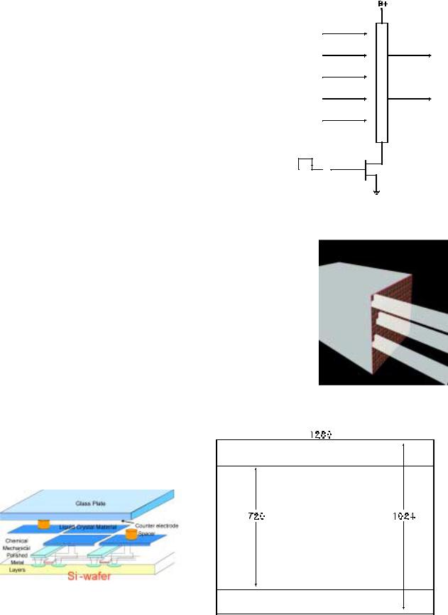
REFLECTIVE LCD PROJECTION SYSTEM |
|
The LCOS (Liquid Crystal on Silicon) uses a reflective LCD |
|
system. A single reflective LCD panel with multiple LCD |
|
cells is used. Since a single panel is used, it is necessary |
|
to scan the panel with the primary colors to obtain a color |
|
picture. A LCD is a light valve which allows more or less |
|
light through it, depending on the applied voltage. See |
|
Figure 17. |
|
The LCD used in most projectors and direct view LCD TVs |
|
uses a transmissive type of LCD. (Figure 18) Light is pro- |
|
jected to pass through the LCD panel. One of the disad- |
|
vantages of this type of system is that the electronics to |
|
control the LCD cells limit the surface area in which light |
|
can pass. This limits the resolution of the picture and |
FIGURE 17 - LCD CELL |
brightness. |
|
The Reflective type of LCD, like the one used in the LCOS, has the electronics beneath the LCD cells, allowing greater resolution. (Figure 19) The LCD cells are turned On, switching the individual cells. Beneath each cell is a reflective surface. The amount of light reflected from each cell depends on the applied voltage. Since the LCD may be illuminated by all three primary colors at one time, several cells are addressed at once.
The Reflective LCD used in the LCOS projector uses a 1280x1024 device with 20 micron pixels. Since the aspect ratio of the TV is 16x9, the actual area used is 1280x720. (Figure 20)
Regardless of the format of the input, the LCD displays the picture in a 1280x720 format.
FIGURE 18 -
TRANSMISSIVE LCD
FIGURE 20 - LCD SURFACE AREA
FIGURE 19 - REFLECTIVE LCD
Page 6

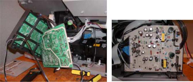
The Philips LCOS projector uses a single LCD device. To obtain a color picture, the LCD is scanned with strips of Red, Green, and Blue light. The strips of color are developed by splitting the light from the Lamp and directing it to three color filters which produce Red, Green, and Blue light. The output from the filters is directed to three rotating Prisms to produce the color strips and direct it to the correct part of the LCD. Data is directed to the LCD in such a way that the correct data for color illuminating that portion of the LCD will be displayed. The LCD is being scanned a rate of 180 Hz. The phase of each prism is offset by 30 degrees to provide color separation. The reflected light from the LCD is fed to a projection lens, the mirror, and finally the screen.
LIQUID
CRYSTAL
DISPLAY
LIGHT SENSOR
LAMP
SCANNING PRISM
DRIVER
PROJECTION LENS
LAMP
LIGHT ENGINE LIGHT PATH
PRISM
Page 7 LIGHT ENGINE WITHOUT LAMP AND PC BOARD
POWER SUPPLY BLOCK (Figure 21)
The Bridge Rectifiers, On/Off Relay, Audio Power supply, and Lamp supply are located on the Power Input board. The Standby and Main supplies are located on the Main Power board.
AC is applied to the Power Input Board via connector 1212. This voltage is rectified to produce the RAWDC-STBY and is fed to the Main Power Board. This feeds the Standby Supply that produces a +5V2 supply. This supply feeds the Power Relay on the Power Input board and the SSB to power the Microprocessor.
The AC input voltage is also fed to a Switch controlled by the Microprocessor on the SSB via the System Board. When the set is turned On, the Standby line goes Low, switching the Relay On. This is fed to a rectifier that supplies RAW_DC to the Audio Supply and Lamp Supply located on the Power Input Board. The rectifier is connected as a voltage doubler. It also supplies RAW_DC to the Main Supply located on the Main Power Board. The Audio Supply provides a positive and negative voltage to the Audio Amplifier Board. The Lamp Supply is a Boost regulator that supplies 330 volts to the Lamp Driver board.
The Main Supply produces a +36, a +12, a +22 and a +9 volt supply. The +9 volt supply is also fed to a 3.3 volt regulator.
AC INPUT (Figure 22)
AC power is connected to the Power Input board via connector 1212. Fuse 1211 provides protection against overcurrent. Spark gaps 1214 and 1216 provide protection against excessive voltage spikes on the AC line. Resistors 3207, 3210, 3213, and 3215 limit the current when power is first applied to the set. Bridge 6202 rectifies the AC voltage to produce the RAWDC_STBY for the Standby regulator.
Bridge 6201 provides power for the Lamp Supply and the Main Power supply. When the set is turned On, Relay 1210 switches On to provide power to 6201. Bridge 6201, Capacitors 2202 and 2209 constitute a voltage doubler circuit. When the set is turned On, the Standby line goes Low. Transistor 7212 turns On turning transistor 7211 On, switching the Relay 7210 On. The ground side of the Relay is connected to the Lamp Door Interlock switch and the Thermal switch which is located on the Lamp Housing. If the Projection Lamp Door is open or the Lamp Housing has overheated, the set cannot be turned On.
Page 8

POWER INPUT BOARD
MAIN POWER BOARD
POWER BOARD SERVICE
POSITION
Page 9

FIGURE 21 - POWER SUPPLY BLOCK |
Page 10 |

Page 11 |
FIGURE 22 - AC INPUT CIRCUIT |
STANDBY SUPPLY (Figure 23)
The Standby supply is located on the Main Power board. It provides the +5VSTBY supply to the set whenever power is applied.
When power is first applied, the RAWDC_STBY is applied to the primary winding of 5210 and to Pin 7 of 7202. Current through resistor Rs charges Capacitor 2244 connected to Pin 1 of 7202. When the charge on 2244 reaches 5.8 volts, the Internal Supply switch is switched to internal. The Oscillator and PWM turn On to drive the internal FET. The PWM will continue to drive the FET until the charge on Capacitor 2244 drops below 4.8 volts. Capacitor 2244 will again charge and the process will repeat. With each startup cycle, energy is transferred to the secondary windings of 5210. When the +5VSTBY supply reaches 5 volts, the input of 7206 will go to 2.5 volts. This will turn Shunt Regulator 7206 On, causing current to flow through optoisolator 6207. Voltage from Pins 1 and 2 of 5210 is rectified by 6205 to produce the operating voltage for 7202. When Optoisolator 6207 turns On, the operating voltage is applied to Pin 1 of 7202. The supply is in a normal operating mode.
Regulation of the secondary is accomplished by monitoring the reference voltage via Shunt Regulator 7206 and optoisolator 6207. The +5VSTBY is the reference voltage for the Standby supply. If the 5-volt standby supply should increase, Shunt Regulator 7206 will conduct harder, causing the LED in Optoisolator 6207 to get brighter. The internal resistance of the transistor inside 6207 will be reduced. The internal regulator inside 7202 connected to Pin 1 works to keep Pin 1 at 5.8 volts. If the current through 6207 increases, the current flow through the 5.8-volt regulator will increase. This increase in current will cause the voltage across the sensing resistor Re to increase. The PWM will then reduce the On time of the internal FET, reducing the secondary voltage. If the 5-volt standby voltage should decrease, the current through the sensing resistor Re will decrease, reducing the voltage across the resistor. This will cause the PWM to turn the internal FET On for a longer period of time, increasing the secondary voltage.
The +5.2 volt supply is switched by FET 7203 when the +12 volt supply from the Main Power supply is switched On. If the Standby Supply should fail or Power is removed from the set, the Standby Power Fail circuit will signal the Microprocessor in time to allow it to shut down. Voltage from Pin 8 of 5210 is rectified by 6209 to produce a negative voltage. This voltage and the +5 volt standby voltage is applied to the input of Shut Regulator 7209. The combined voltage keeps the input to 7209 below the turn On voltage of 2.5 volts. A small Capacitor, 2265, filters the negative voltage that is rectified by 6209. If power is removed from the set, 2265 will discharge quickly because of its small value. The input to 7209 will then go above 2.5 volts, turning it On. This will turn transistor 7210 On, switching the Standby Power Fail line High. Transistor 7210 will also turn On, turning the +5.2 volt supply Off.
Page 12

Page 13 |
FIGURE 23 - STANDBY SUPPLY |
MAIN POWER SUPPLY (Figure 24)
Power is applied to the Main Power supply when the set is turned On. The RAW-DC is switched to the Main Power supply located on the Main Power supply board. Voltage is applied to the Primary winding of 5310 via Pins 5 and 3. Voltage is then applied to Pin 7 of 7302. In the Startup mode, voltage from the internal current limiting resistor Rs is routed to Pin 1 where it charges Capacitor 2344. When the charge on Capacitor 2344 reaches 5.8 volts, Pin 1 is switched to the Internal Supply connection. The Oscillator and PWM drive are switched On to drive 5310. IC 7302 will continue to drive the Transformer, 5310, until the charge on 2344 drops below 4.8 volts. The Startup cycles will continue until the secondary reference voltage, the 9 volts supply, reaches the correct level. When the 9-volt supply reaches the correct level, 2.5 volts will be applied to the input of Shunt Regulator 7306. Shunt Regulator 7306 will then turn On causing current to flow through the LED in Optoisolator 6307. This will turn the transistor inside 6307 to turn On. Voltage from Pins 1 and 2 of the Hot secondary is rectified by 6305 and filtered by 2341. Optoisolator 6307 switches this voltage to Pin 1 of 7302 to provide the operating voltage for the IC.
The secondary produces +36, +12, +9, and +22 volt supplies. Shunt Regulator 7304 and FET 7303 regulate the +12 volt supply.
The PWR_FAIL Main Power Fail detection circuit signals the Microprocessor when power is about to be lost to the set while it is On. Voltage from Pin 9 of 5310 is rectified by 6309 to produce a negative voltage, which is filtered by Capacitor 2365. This voltage along with the +9 volt supply is applied to the input of Shunt regulator 7309 via resistor network of 3354, 3355, and 3353. As long as the negative voltage is present on 2365, the voltage on the input of 7309 will be less than the 2.5 volts necessary to turn it On. Transistor 7310 will be turned Off, keeping the PWR_FAIL line Low. When the switched mode supply ceases operation, Capacitor 2365 will discharge quickly, due to its low value, allowing the voltage on the input of 7309 to increase to 2.5 volts. Shunt Regulator 7309 will turn On, turning transistor 7310 On, causing the PWR_FAIL line to go High. This will signal the Microprocessor to shut everything down before the main supply voltage drops.
Regulation of the secondary is accomplished by monitoring the reference voltage, the +9 volt supply, to control the On time of the internal FET of 7302. If the +9 volt supply increases, Shunt Regulator 7306 will conduct harder increasing the amount of current through 6307. This will cause the LED to increase in brightness, reducing the internal resistance of the transistor inside the IC. The increase in current will cause the voltage across the internal sensing resistor Re inside 7302 to increase. The PWM will then reduce the On time of the internal FET, decreasing the secondary voltage. If the +9 volt supply should decrease, 7306 will conduct less, the transistor inside 6307 will conduct less, causing less current to flow through the sensing resistor Re. The PWM will sense the lower voltage across Re, increasing the On time of the internal FET to increase the secondary voltage.
Page 14

Page 15 |
FIGURE 24 - MAIN POWER SUPPLY |
3.3 VOLT REGULATOR (Figure 25)
IC 7307 and transistor 7308 make up the 3.3-volt regulator located on the Main Power Supply board. When the Oscillator in 7307 goes Low, the flip-flop is reset causing Q to go Low and the output to go High. When the Feedback voltage on Pin 5 is below 1.25 volts, the comparator outputs a High. When the Oscillator goes High, the flip-flop is Set, causing Q to go High. This causes Pin 1 to go Low, turning Transistor 7308 On. 7308 will stay on until the Oscillator goes Low, resetting the flip-flop. If the output voltage monitored on Pin 5 goes below 3.3 volts, the voltage on Pin 5 will drop below the 1.25 volt reference. The flip-flop will then Set when the Oscillator goes High. If the output voltage goes above 3.3 volts, the reference voltage on Pin 5 will be above the 1.25 volt internal reference. The flip-flop will not Set when the Oscillator goes High until the feedback reference voltage on Pin 5 drops below the 1.25 volt internal reference. This method controls the On time of 7308 to regulate the 3.3-volt supply. Pin 7 monitors the current by reading the voltage drop across resistors 3349 and 3351. If the output current is excessive, the Oscillator will go Low to shorten the On time of 7308.
POWER INPUT BOARD IN SERVICE POSITION |
MAIN POWER BOARD |
Page 16

Page 17 |
FIGURE 25 - 3.3-VOLT REGULATOR |
AUDIO POWER SUPPLY (Figure 26)
The Audio supply produces a plus and minus 23 volts. This supply is located on the Power Input board. The Audio supply also produces the CONTROL-VOLTAGE or operating voltage for the Lamp supply.
RAW-DC voltage is applied to the Audio Power supply circuit when the set is turned On. This voltage is applied to primary windings, Pins 5 and 3, of Transformer 5410. It is also applied to Pin 7 of the Switching Regulator, IC 7402. Startup occurs when the voltage applied to Pin 7 is fed to the current limiting resistor Rs and to Pin 1 of the IC. This voltage charges Capacitor 2444. When the voltage on this Capacitor reaches 5.8 volts, Pin 1 is switched to the Internal Supply. The Oscillator and PWM drive turns On to drive the internal FET. This drives 5410 to produce the secondary voltages. The IC will continue to operate until the charge on 2444 drops below 4.8 volts. The Startup cycle will then repeat. When the secondary voltages have reached the correct level, the input to Shunt Regulator 6404 will increase to 2.5 volts. Shut Regulator 7406 will then turn On, switching Optoisolator 6404 On. The voltage on Pin 1 and 2 of 5410 is rectified by 6405 and filtered by Capacitor 2441. This voltage is then switched by Optoisolator 6404 to Pin 1 of 7402 to provide the operating voltage. The supply is then operating in a normal mode. The operating voltage from 6405 is also used to supply the CONTROL-VOLTAGE supply to the Lamp supply.
Regulation is accomplished by monitoring the Positive Audio supply. This voltage is fed to resistor network, 3444, 3445, and 3438. It is then fed to the input of Shunt Regulator 7406. If the secondary voltage should increase, Shut Regulator 7406 will conduct harder, increasing the current through the LED in Optoisolator 6404. This will decrease the internal resistance of the Transistor inside 6404. The 5.8-volt regulator inside 7402 keeps Pin 1 at 5.8 volts. To maintain this Pin at the correct voltage, the Regulator will increase the current through the sensing resistor Re. The voltage across Re is fed to the PWM which reduces the On time of the Internal FET, which reduces the output voltage. If the secondary voltage should decrease, the voltage across Re would decrease via the same path. The PWM would then increase the On time of the internal FET to increase the secondary voltage. In some cases, the secondary load could become excessive on the positive supply causing the voltage on the other windings of 5410 to increase. If the voltage from Pin 1 of 5410 should exceed 23.8 volts, Zener diode 6404 will conduct, increasing the current through the sensing resistor Re to reduce the On time of the internal FET to prevent damage to the supply.
The Audio supply can also be shut down if a DC-FAULT is detected in the Audio Output circuit or if the positive and negative supplies become unbalanced. In normal operation, the DCFAULT line is Low, turning Transistor 7412 On. This turns Transistor 7411 On, which turns on Optoisolator 6410. This connects resistor 3403 and Pin 3 of 7402 to ground. This enables the Switching Regulator IC 7402. If Pin 3 is open, 7402 will shut down. If the DC_FAULT line should go High, 7412 will turn Off, turning 7411 and the Optoisolator 6410 Off. This will shut the supply down. The positive supply is connected to diodes 6407 and 6409 via resistor 3460. The negative supply is also connected to the same point. When the supplies are equal, the voltage at this point is zero. If the voltage becomes unbalanced in the negative direction by - 2.5 volts, Transistor 7410 will turn On, turning Transistor 7409 On. This will turn Transistor 7411 Off, shutting the supply Off. If the voltage becomes unbalanced in the positive direction by 1.2 volts, Diode 6409 will conduct, turning Transistor 7409 On, turning 7411 Off, shutting
the supply down.
Page 18

19 Page
SUPPLY POWER AUDIO - 26 FIGURE
OPERATING VOLTAGE FOR THE LAMP SUPPLY REGULATOR
LAMP SUPPLY (Figure 27)
The Projection requires a minimum of 330 volts to operate. To ensure that sufficient voltage is present, a Boost Regulator is used. A Boost Regulator has a higher output voltage than the input voltage. The Lamp supply is located on the Power Input board.
RAW-DC-LAMP is applied to the Boost circuit via Fuse 1511. Voltage is applied to Pin 1 and Capacitor 2544 via the current limiting resistor Rs in 7502. When the charge on 2544 reaches 5.8 volts, the PWM circuit drives the internal FET. When the FET is On, a field builds up in Coil 5510. 5509 is a Ferrite bead to reduce RFI. When the FET turns Off, the field in 5510 reverses. This voltage is rectified by Diode 6501, which charges Capacitor 2534. This will continue until the charge on 2544 drops below 4.8 volts. The Startup cycle will then repeat. When the voltage across 2534 reaches 330 volts, Shunt Regulator 7506 turns On, turning Transistor 7500 On. The Control Voltage from the Audio Power supply now becomes the operating voltage for Pin 1 of 7502.
Regulation is accomplished by the monitoring of the 330 Lamp voltage by Shunt Regulator 7506. If the 330-volt supply increases, 7506 will turn On harder, turning Transistor 7500 On harder. The increase in current will increase the voltage across the sensing resistor Re inside 7502. The Regulator connected to Pin 1 will keep Pin 1 at a constant 5.8 volts. The voltage across Re will be fed to the PWM, reducing the On time of the internal FET to reduce the output voltage.
If the Switch mode circuit for the Lamp supply failed to operate, the voltage to the Lamp would be equal to the RAW-DC-LAMP voltage. The symptom is this case would be that the lamp would not ignite. Another possibility would be that 7502 might short. There would not be Lamp voltage in this case. A Low output voltage might be caused by the feedback circuit, 7506 and 7500, failing to operate. A Scope reading on Pin 1 of 7502 would indicate that the voltage would be changing between 4.8 and 5.8 volts. Pin 7 of 7502 would be pulsing On and Off.
Page 20

Page 21 |
FIGURE 27 - LAMP SUPPLY |

VIDEO SIGNAL FLOW BLOCK (Figure 28)
The LCOS projector has three sections:the 1FH NTSC processing, Scaler HD Processing, and the Light Engine.
The 1FH NTSC section has three video inputs, AV1, AV2, and Side, which are for NTSC composite video only. This section has Line Doubling, Pixel Plus, and Picture in Picture functions. The 2FH signal from this section is fed to the Scaler HD Processing section.
The Scaler HD Processing section has two Y Pb Pr inputs, AV3 and AV4. AV5 is a RGB input while AV6 is a DVI input. AV3 and AV4 can accept either a 1H NTSC signal, a 480P signal, or a 1080I HD signal. For best results, the 1FH signals should be connected to AV1, AV2, or the Side input. It also processes the 2FH signal from the 1FH NTSC section. The Signal is processed to output a 1280x720 pixel to the Light Engine. The Light Engine contains all of the display circuits used to project the picture to the screen.
1FH PROCESSING IS FOR NTSC ONLY
PIXEL PLUS PROCESSING IN THE 1FH SECTION
EITHER 1FH OR 2FH SIGNAL CAN BE APPLIED TO THE SCALER
REGARDLESS OF THE SOURCE ALL SIGNALS ARE
DISPLAYED IN A 1280x720 FORMAT
FIGURE 28 - VIDEO SIGNAL FLOW BLOCK |
Page 22 |

FIGURE 29 - OVERALL BLOCK 1FH SECTION (Figure 29)
The inputs for the 1FH section are for NTSC signals only. The Side Jack panel can accept either composite video or SVHS video. The Composite video or YC from the Side Jack Panel is fed to the Jack Panel. Two Composite or SVHS inputs, AV1 and AV2 are located on the Jack Panel. These inputs, along with the input from the Side Jack panel, are fed to the 7100 switch. IC 7100 selects between the three composite or SVHS inputs for output to the SSB and PIP/DW boards via the System board. A Y Pb Pr 1FH input is also located on the Jack Panel. This signal is converted from Y Pb Pr to YUV on the System board before being fed to the SSB. This YUV signal is also fed to the PIP/DW panel. IF from the main Tuner, located on the System board, is also fed to the SSB.
The HIP IC on the SSB selects between the internal Tuner video or selected video from the Jack panel. If the signal is Composite video, it is fed to a 3D Comb filter panel for processing. YC from the 3D Comb filter is fed back to the HIP. The HIP then outputs YUV to the PIP/DW panel, which inserts the Picture in Picture or Split Screen when selected by the customer. The Picture in Picture or Split Screen video is selected from the YUV signal, the selected video from the Jack Panel switch, or the Tuner located on the PIP/DW panel. YUV from the PIP/DW is then fed to the Feature Box, which performs the line doubling and zooming features. YUV from the Feature Box is then fed to the Eagle circuit, which enhances the picture. The Pixel Plus feature is performed in the Eagle if the set is programmed for the Pixel Plus feature. The YUV output from the Eagle is then fed to the LVDS transmitter before being sent to the Scaler board. The video signal is digitized in the Feature Box and remains digitized from that point on.
SSB SMALL SIGNAL BOARD |
MSB MAIN SCALER BOARD |
JACK PANEL |
JACK PANEL BOARD |
Page 23
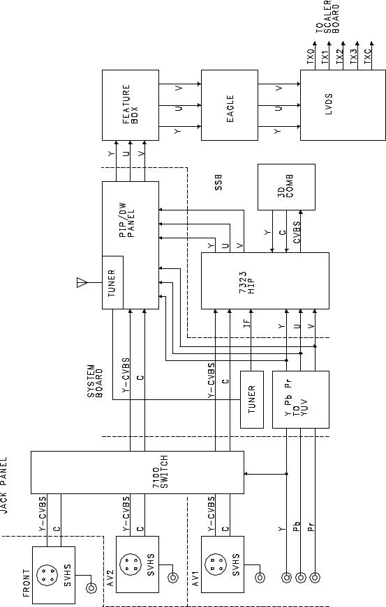
FIGURE 29 - OVER BLOCK - 1FH SECTION |
Page 24 |
SIDE JACK PANEL (Figure 30)
The Side Jack panel can have either a composite or SVHS input. When a connector is inserted into the SVHS input, the composite input is disconnected. Zener diodes are connected to both the Y/composite and the C lines to limit the applied voltage to 7.4 volts. A 75ohm resistor on both lines provides the correct impedance matching. The Y/composite and C signals are output to the Jack panel via the System board.
FIGURE 30 - SIDE JACK PANEL VIDEO
SIDE JACK PANEL
Page 25

AV1 INPUT (Figure 31)
The AV1 and AV2 inputs are located on the Jack panel. Composite video for AV1 is input to connector 1251 and then to an impedance matching network consisting of resistors 3248 and 3182. Diode array 6126 prevents the incoming signal from exceeding 9.6 volts in the positive direction and 0.6 volts in the negative direction. When a connector is placed in the SVHS jack, the Composite video input is disconnected. The Y signal is routed through an impedance matching network and clamp and back to Pin 11 of 1218. The C signal is also routed through an impedance matching network, clamped to Pin 6, and output on Pin 5. The clamping voltage +Vp is supplied by the +9 volt source. The AV2 input is identical except for the component input.
FIGURE 31 - AV1 INPUT CIRCUIT
Page 26

1H COMPONENT INPUT (Figure 32)
The 1FH Y Pb Pr inputs are located on the Jack panel. The 1H Y Pb Pr inputs all have an impedance matching resistor and clamping circuit. As with the composite and SVHS inputs, the input signal is clamped to be no more that 0.6 volts above the +Vp supply in the positive direction and no more than 0.6 volts in the negative direction. The clamping voltage +Vp is supplied by the +9 volt source. The Y signal is also fed to IC 7100 for Sync separation.
The Y Pb Pr signals are fed to the System board via connector 1220. The circuit on the System Board converts the signals from a Y Pb Pr format to a YUV format. To provide proper impedance matching, Transistors 7002 and 7006 buffer the Y signal. Transistors 7001 and 7005 phase invert the Pb signal to convert it to a U signal. Transistors 7003 and 7007 phase invert the Pr signal to convert it to a V signal. The converted YUV signals are fed to the SSB.
FIGURE 32 - 1FH COMPONENT INPUT CIRCUIT
Page 27
 Loading...