


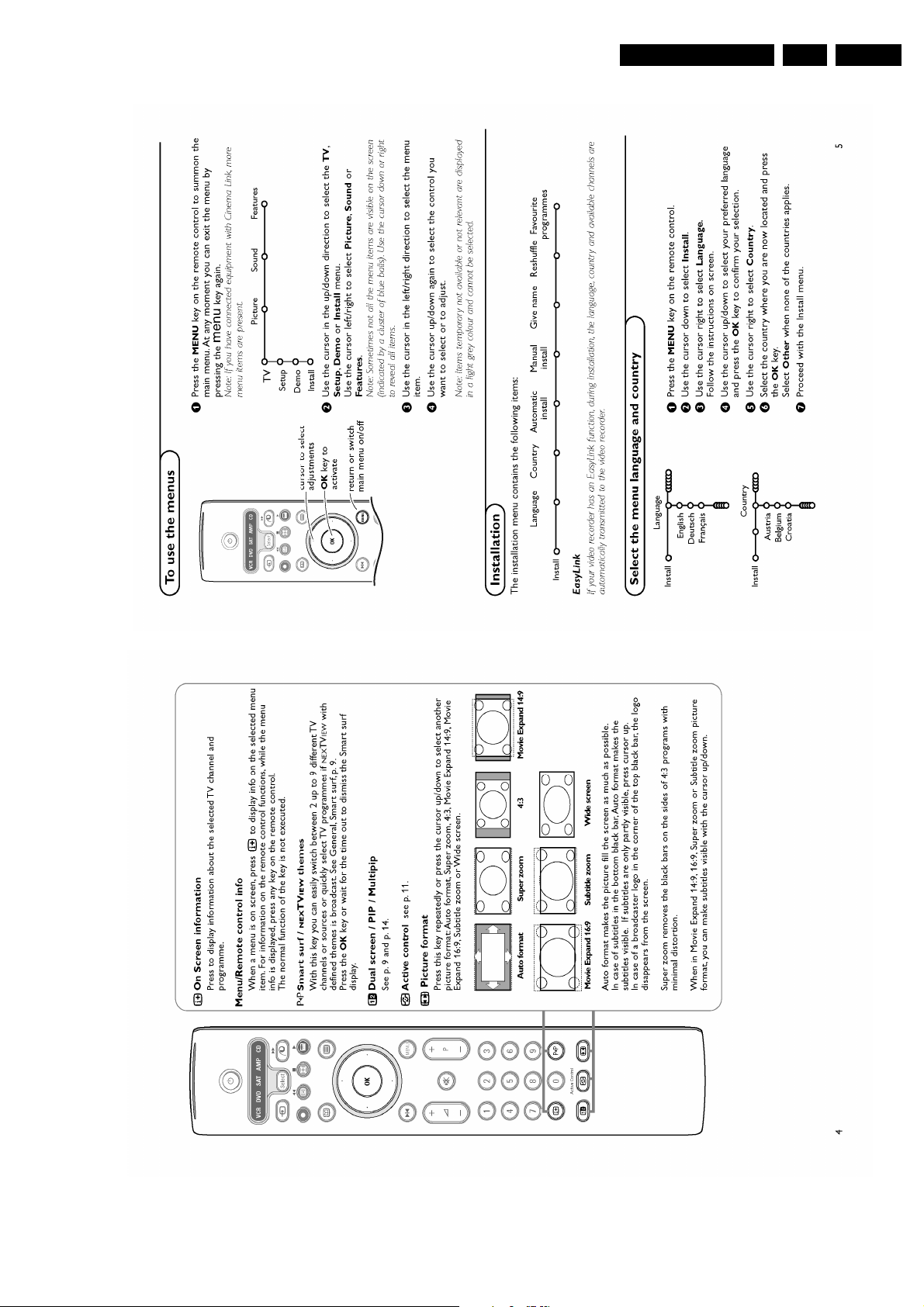
EM5.1E AA
Table of contents
 Loading...
Colour Television Chassis
EM5.1E
AA
CL 36532017_000.eps
240403
Contents Page Contents Page
1. Technical Specifications, Connections and
Chassis Overview 2
2. Safety & Maintenance Instructions, Warnings and
Notes 5
3. Directions for Use 6
4. Mechanical Instructions 17
5. Service Modes, Error Codes and Faultfinding 21
6. Block Diagram, Testpoints, and Overviews
Wiring Diagram 33
Block Diagram Supply and Deflection 34
Block Diagram Video 35
Block Diagram Audio 1 (Excl Wireless Audio) 36
2
I
C-IC Overview 37
Supply Lines Overview 38
Testpoint Overview LSP & CRT/Auto SCAVEM 39
Testpoint Overview SSB 40
7. Electrical Diagrams and PWB’s Diagram PWB
Main Supply (Diagram A1) 41 50-56
Stand-by Supply (Diagram A2) 42 50-56
Line Deflection (Diagram A3) 43 50-56
Frame Deflection & E/W Drive (Diagram A4) 44 50-56
Rotation Circuitry (Diagram A5) 45 50-56
Audio Amplifier (Diagram A6) 46 50-56
Tuner SIMM connector (Female) (Diagram A8) 47 50-56
Receiver (Diagram A9) 48 50-56
Front (Diagram A10)48 50-56
Inputs/Outputs (Diagram A11)49 50-56
SIMM connector (Male) (Diagram B1) 57 68-73
IF, I/O Videoprocessing (Diagram B2) 58 68-73
PICNIC (Diagram B3A)59 68-73
Diversity Tables SSB (Not Applicable Yet) 60 68-73
Falconic (Diagram B3B)61 68-73
Eagle (Diagram B3C)62 68-73
HOP (Diagram B4) 63 68-73
©
Copyright 2003 Philips Consumer Electronics B.V. Eindhoven, The Netherlands.
All rights reserved. No part of this publication may be reproduced, stored in a
retrieval system or transmitted, in any form or by any means, electronic,
mechanical, photocopying, or otherwise without the prior permission of Philips.
OTC (Diagram B5) 64 68-73
Audio Demodulator (Diagram B6) 65 68-73
Anti Moiré (Diagram B9) 66 68-73
Headphone Amplifier (Diagram B10)67 68-73
DW Panel: Multi PIP Controller (Diagram C1) 74 78
DW Panel: Tuner (Diagram C2) 75 78
DW Panel: I/O Processing (Diagram C3) 76 78
DW Panel: IF Video Sync (Diagram C4) 77 78
Mains Switch Panel (FL11 Styling)(Diagram E) 79 80
Mains Switch Panel (PV2 Styling)(Diagram E) 81 82
CRT (FL11 Styling) (Diagram F1) 83 85-86
CRT/Auto Scavem (FL11 Styling)(Diagram F2) 84 85-86
CRT (PV2 Styling) (Diagram F) 87 88-89
DC Shift Panel (Diagram G) 90 90
I/O 3rd SCART Panel (Diagram H) 91 92
VDAF + 2nd Orders Panel (Diagram I) 93 94
Side I/O Panel (FL11 Styling) (Diagram O) 95 96
Side I/O Panel (PV2 Styling) (Diagram O) 97 98
Top Control (FL11 Styling) (Diagram P) 99 99
Top Control (PV2 Styling) (Diagram P) 100 100
Auto SCAVEM (Diagram SC1)101 102
8. Alignments 103
9. Circuit Description 112
Abbreviation List 116
IC Data Sheets 119
10 Spare Parts List 120
11 Revision List 134
Published by WO 0364 Service PaCE Printed in the Netherlands Subject to modification EN 3122 785 13420
EN 2 EM5.1E1.
Technical Specifications, Connections and Chassis Overview
1. Technical Specifications, Connections and Chassis Overview
1.1 Technical Specifications
1.1.1 Vision
Display type : CRT, Real Flat WS
Screen size : 28” (70 cm)
: 32" (82 cm)
: 36” (92 cm)
Tuning system : PLL
Colour systems : PAL B/G, D/K, I
: SECAM B/G, D/K, L/L’
: NTSC playback only
Channel selections : 100 presets
: UVSH
Aerial input : 75 ohm, IEC-type
1.1.2 Sound
Sound systems : FM-mono
: AM-mono
: FM-stereo B/G,
Czech
: NICAM B/G, D/K, I, L
Maximum power : 4 x 15 W rms (int.)
1.1.3 Miscellaneous
Mains voltage : 220 - 240 V
Mains frequency : 50 / 60 Hz
Ambient temperature : +5 to +45 deg. C
Maximum humidity : 90 % R.H.
Power consumption : ?
- Normal operation : ≈ 130 W
- Standby : < 1 W
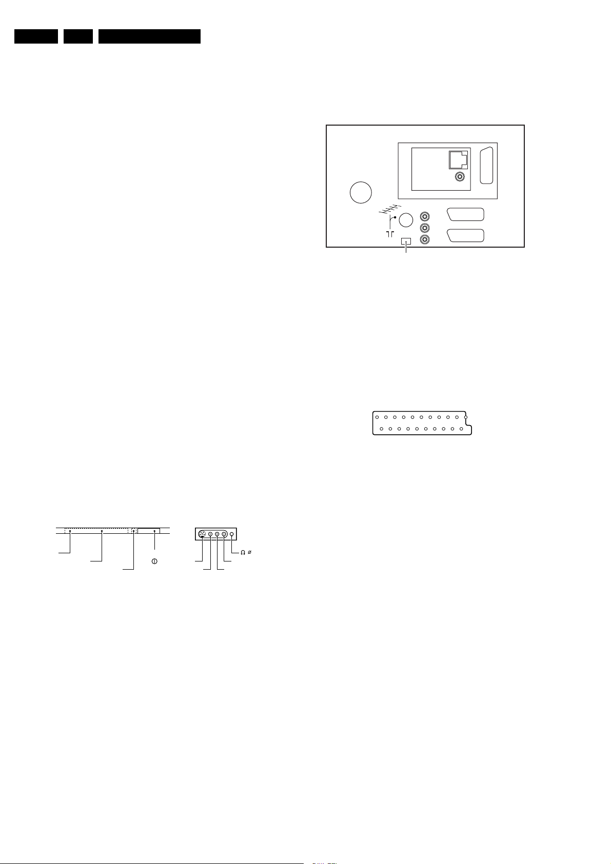
1.2.2 Rear Connections
AUDIO OUT
SERVICE
CONNECTOR
Figure 1-2 Rear View
Aerial - In
- IEC-type Coax, 75 ohm
Cinch: Audio - Out
- Audio - R 0.5 Vrms / 1 kohm
- Audio - L 0.5 Vrms / 1 kohm
External 1: RGB/YUV and CVBS - In/Out
121
CL96532137_056.eps
SURR.
SURR.
L
R
EXT3
EXT1
EXT2
CL 26532041_071.eps
202
171199
110402
1.2 Connections
1.2.1 Front View / Side Connections
IR-RECEIVER
STANDBY LED
SK 1LIGHT SENSOR
Figure 1-1 Front View and Side I/O
Hosiden: SVHS - In
1 - Y Ground
2 - C Ground
3 - Y 1 Vpp / 75 ohm
4 - C 0.3 Vpp / 75 ohm
Cinch: In
1 - CVBS 1 Vpp / 75 ohm
2 - Audio - L 0.5 Vrms / 10 kohm
3 - Audio - R 0.5 Vrms / 10 kohm
Mini Jack: Headphone - Out
- Headphone 32 - 600 ohm / 10 mW
SVHS
VIDEO
CL 26532041_070.eps
AUDIO R
AUDIO L
110402
Figure 1-3 SCART connector
1 - Audio - R 0.5 Vrms / 1 kohm
2 - Audio - R 0.5 Vrms / 10 kohm
3 - Audio - L 0.5 Vrms / 1 kohm
4 - Audio Ground
3.5
5 - Audio Ground
6 - Audio - L 0.5 Vrms / 10 kohm
7 - Blue / U 0.7 Vpp / 75 ohm
8 - CVBS-status 0 - 1.3 V: INT
4.5 - 7 V: EXT 16:9
9.5 - 12 V: EXT 4:3
9 - Video Ground
10 - n.c.
11 - Green / Y 0.7 Vpp / 75 ohm
12 - n.c.
13 - Video Ground
14 - Video Ground
15 - Red / V 0.7 Vpp / 75 ohm
16 - Status / FBL 0 - 0.4 V: INT
1 - 3 V: EXT / 75 ohm
17 - Video Ground
18 - Video Ground
19 - CVBS-out 1 Vpp / 75 ohm
20 - CVBS-in 1 Vpp / 75 ohm
21 - Shielding Ground
Technical Specifications, Connections and Chassis Overview
EN 3EM5.1E 1.
External 2: CVBS and SVHS - In (for VCR)
121
CL96532137_056.eps
202
171199
Figure 1-4 SCART connector
1 - Audio - R 0.5 Vrms / 1 kohm
2 - Audio - R 0.5 Vrms / 10 kohm
3 - Audio - L 0.5 Vrms / 1 kohm
4 - Audio Ground
5 - Audio Ground
6 - Audio - L 0.5 Vrms / 10 kohm
7 - C-out 0.7 Vpp / 75 ohm
8 - CVBS-status 0 - 1.3 V: INT
4.5 - 7 V: EXT 16:9
9.5 - 12 V: EXT 4:3
9 - Video Ground
10 - Easylink (P50)
11 - n.c.
12 - n.c.
13 - Video Ground
14 - Video Ground
15 - C-in 0.7 Vpp / 75 ohm
16 - n.c.
17 - Video Ground
18 - Video Ground
19 - CVBS-out 1 Vpp / 75 ohm
20 - Y / CVBS-in 1 Vpp / 75 ohm
21 - Shielding Ground
3 - GND Ground
4 - I2C_MUTE Signal
5 - 15V Supply
6 - AUDIO_
SL_S_TM Signal
7 - GND_AUD Ground
8 - PILOT_MUTE Signal
Jack: Surround - Out
1 - Audio 0.2 - 2 Vrms / 10 kohm
External 3: RGB and CVBS - In
121
CL96532137_056.eps
202
171199
Figure 1-5 SCART connector
1-n.c.
2 - Audio - R 0.5 Vrms / 10 kohm
3-n.c.
4 - Audio Ground
5 - Audio Ground
6 - Audio - L 0.5 Vrms / 10 kohm
7 - Blue-in 0.7 Vpp / 75 ohm
8 - CVBS-status 0 - 1.3 V: INT
4.5 - 7 V: EXT 16:9
9.5 - 12 V: EXT 4:3
9 - Video Ground
10 - n.c.
11 - Green-in 0.7 Vpp / 75 ohm
12 - n.c.
13 - Video Ground
14 - Video Ground
15 - Red-in 0.7 Vpp / 75 ohm
16 - Status / FBL 0 - 0.4 V: INT
1 - 3 V: EXT / 75 ohm
17 - Video Ground
18 - Video Ground
19 - n.c.
20 - CVBS-in 1 Vpp / 75 ohm
21 - Shielding Ground
RJ45: Wireless Surround Transmitter - Out
1 - SDA2_TM Signal
2 - SCL2_TM Signal

EN 4 EM5.1E1.
1.3 Chassis Overview
Technical Specifications, Connections and Chassis Overview
CRT PANEL
F
SIDE I/O PANEL
O
SMALL SIGNAL BOARD
B
C
PIP/DOUBLE
WINDOW PANEL
(optional)
AUTO-SCAVEM
SC
I/O 3rd SCART
H
TOP CONTROL PANEL
MAINSWITCH PANEL
LARGE SIGNAL PANEL
DC-SHIFT (optional)
DAF PANEL
P
P
E
A
G
I
Figure 1-6 PWB location
CL 36532017_054.eps
240403

Safety Instructions, Warnings, and Notes
2. Safety Instructions, Warnings, and Notes
EN 5EM5.1E 2.
2.1 Safety Instructions
Safety regulations require that during a repair:
• Connect the Receiver box to the Mains via an isolation
transformer.
• When you use the Receiver box in combination with a
plasma monitor, do not operate the monitor without the
front glass plate. One function of this glass plate is to
absorb IR radiation. Without this glass plate, the level of
radiation could damage your eyes.
• Safety components, indicated by the symbol , must be
replaced with original components.
Safety regulations require that after a repair, you must return
the set in its original condition. Pay particular attention to the
following points:
• Route the wire trees in their original positions and fix them
in place with the mounted cable clamps.
• Check the insulation of the Mains cord for external
damage.
• Check the electrical DC resistance between the Mains plug
and the secondary side (only for sets which have a Mains
isolated power supply):
– Unplug the Mains cord and connect a wire between the
two pins of the Mains plug;
– Set the Mains switch to the "on" position (keep the
Mains cord unplugged!).
– Measure the resistance value between the pins of the
Mains plug and the metal shielding of the tuner or the
aerial connection on the set. The reading should be
between 4.5 Mohm and 12 Mohm.
– Set the Mains switch to the "off" position, and remove
the wire between the two pins of the Mains plug.
• Check the cabinet for defects, to prevent the customer from
touching any inner parts of the television set.
2.2 Warnings
• All ICs and many other semiconductors are susceptible to
electrostatic discharges (ESD symbol ). Careless
handling during repair can reduce life drastically. Make
sure that, during repair, you are connected with the same
electrical potential as the set by a wristband with
resistance. Keep components and tools at this same
potential. Available ESD protection equipment:
– Complete ESD3 kit (small tablemat, wristband,
connection box, extension cable and earth cable):
4822 310 10671.
– Wristband tester: 4822 344 13999.
• Be careful while taking measurements in the live voltage
section.
• Never replace modules, or other components, with the
television set "'ON."
• Use plastic tools, instead of metal tools, when performing
alignments on the television set. This will help prevent
short circuits and reduce the danger of a circuit becoming
unstable.
stereo sound (L: 3 kHz, R: 1 kHz unless stated otherwise)
and picture carrier at 61.25 MHz (NTSC).
• Where necessary, measure the oscillograms and direct
voltages with (symbol ) and without (symbol ) aerial
signal. Measure the voltages in the power supply section
both in normal operation (symbol ) and in standby
(symbol ). These values are indicated by means of the
appropriate symbols.
• The semiconductors indicated in the circuit diagram and in
the parts lists, are interchangeable position with the
semiconductors in the unit, irrespective of the type
indication on these semiconductors.
2.3.2 Schematic Notes
• All resistor values are in ohms and the value multiplier is
often used to indicate the decimal point location (e.g. 2K2
indicates 2.2 kohm).
• Resistor values with no multiplier may be indicated with
either an 'E' or an 'R' (e.g. 220E or 220R indicates 220
ohm).
• All Capacitor values are expressed in Micro-Farads
• Capacitor values may also use the value multiplier as the
• An 'asterisk' (*) indicates component usage varies. Refer to
• The correct component values are listed in the Electrical
2.3.3 Practical Service Precautions
• It makes sense to avoid exposure to electrical shock.
• Always respect voltages. While some may not be
• Before powering up the TV set with the rear cover off
-6
(µ = x10
(p = x10
decimal point indication (e.g. 2p2 indicates 2.2 pF).
the diversity tables for the correct values.
Replacement Parts List. Therefore, always check this list
when there is any doubt.
While some sources are expected to have a possible
dangerous impact, others of quite high potential are of
limited current and are sometimes held in less regard.
dangerous in themselves, they can cause unexpected
reactions - reactions that are best avoided. Before reaching
into a powered TV set, it is best to test the high voltage
insulation. It is easy to do, and is a good service precaution.
(or on a test fixture), attach a clip lead to the CRT DAG
ground and to a screwdriver blade that has a well insulated
handle. After the TV is powered on and high voltage has
developed, probe the anode lead with the blade, starting at
the case of the High Voltage Transformer (flyback - IFT).
Move the blade to within two inches of the connector of the
CRT. If there is an arc, you found it the easy way,
without getting a shock! If there is an arc to the
screwdriver blade, replace the part that is causing the
problem: the High Voltage Transformer or the lead (if it is
removable).
), Nano-Farads (n = x10-9), or Pico-Farads
-12
).
2.3 Notes
2.3.1 General
• Measure the direct voltages and oscillograms with regard
to the chassis ground (symbol ), or hot ground
(symbol ).
• The direct voltages and oscillograms shown in the
diagrams are indicative. Measure them in the Service
Default Mode (see chapter 5) with a colour bar signal and
EN 6 EM5.1E3.
3. Directions for Use
Directions for Use
Directions for Use
EN 7EM5.1E 3.
EN 8 EM5.1E3.
Directions for Use
Directions for Use
EN 9EM5.1E 3.
EN 10 EM5.1E3.
Directions for Use
Directions for Use
EN 11EM5.1E 3.
EN 12 EM5.1E3.
Directions for Use
Directions for Use
EN 13EM5.1E 3.
EN 14 EM5.1E3.
Directions for Use
Directions for Use
EN 15EM5.1E 3.
EN 16 EM5.1E3.
Directions for Use
4. Mechanical Instructions
Mechanical Instructions
EN 17EM5.1E 4.
Index of this chapter:
1. Service Connector
2. Set Disassembly
3. Service Positions
4. Assy / Board Removal
5. Set Reassembly
Note: Figures below can deviate slightly from the actual
situation, due to the different set executions.
4.1 Service Connector (for ComPair)
For service diagnostics with ComPair, it is not necessary to
disassemble the set. You only have to connect the ComPair
interface box, via the appropriate cable, to the service
connector (on the rear of the set, see figure below), and start
the program.
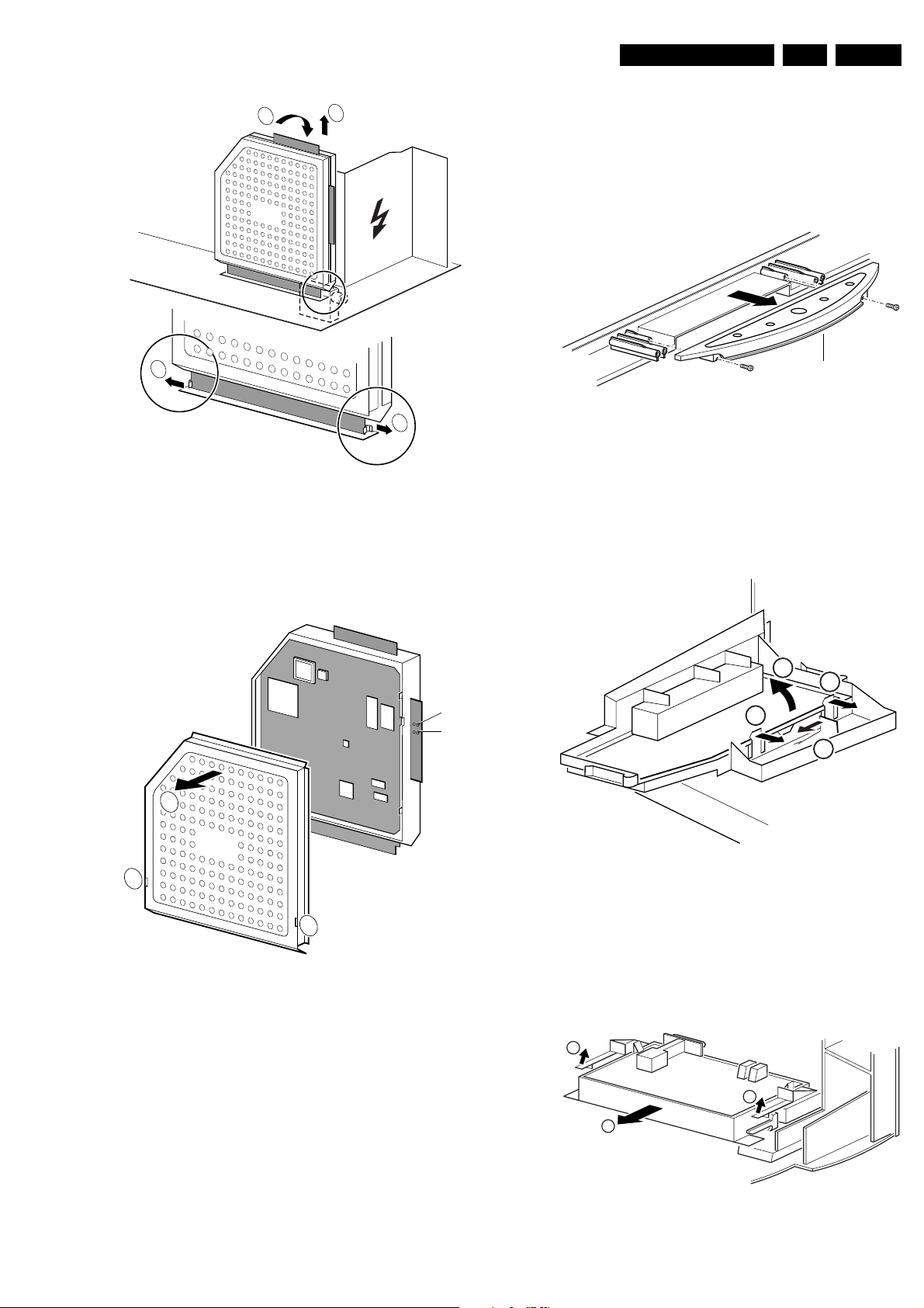
4.2 Set Disassembly
Follow the disassemble instructions in described order.
4.2.1 Wireless Surround Transmitter Removal (if attached)
1. Remove the cable of the Wireless Surround Transmitter
box (at the side of this RJ45 plug you can find the releasehook of the lock-mechanism).
2. Pull the Wireless Surround Transmitter box backwards. It
is clicked to the rear cover via three clamps.
4.2.3 Sub-woofer Removal
Caution: Do not disconnect the loudspeaker cable from the
subwoofer box when the set is operative, because the class-D
amplifier cannot handle a change in load during operation.
It is no problem when the subwoofer is disconnected before
operation, but a change from connected to disconnected
during operation can damage the amplifier.
1. Disconnect the loudspeaker cable connectors at the top of
the sub-woofer box.
2. Unlock he subwoofer bracket and at the same time pull the
unit backwards.
3. Take out the sub-woofer unit including the bracket.
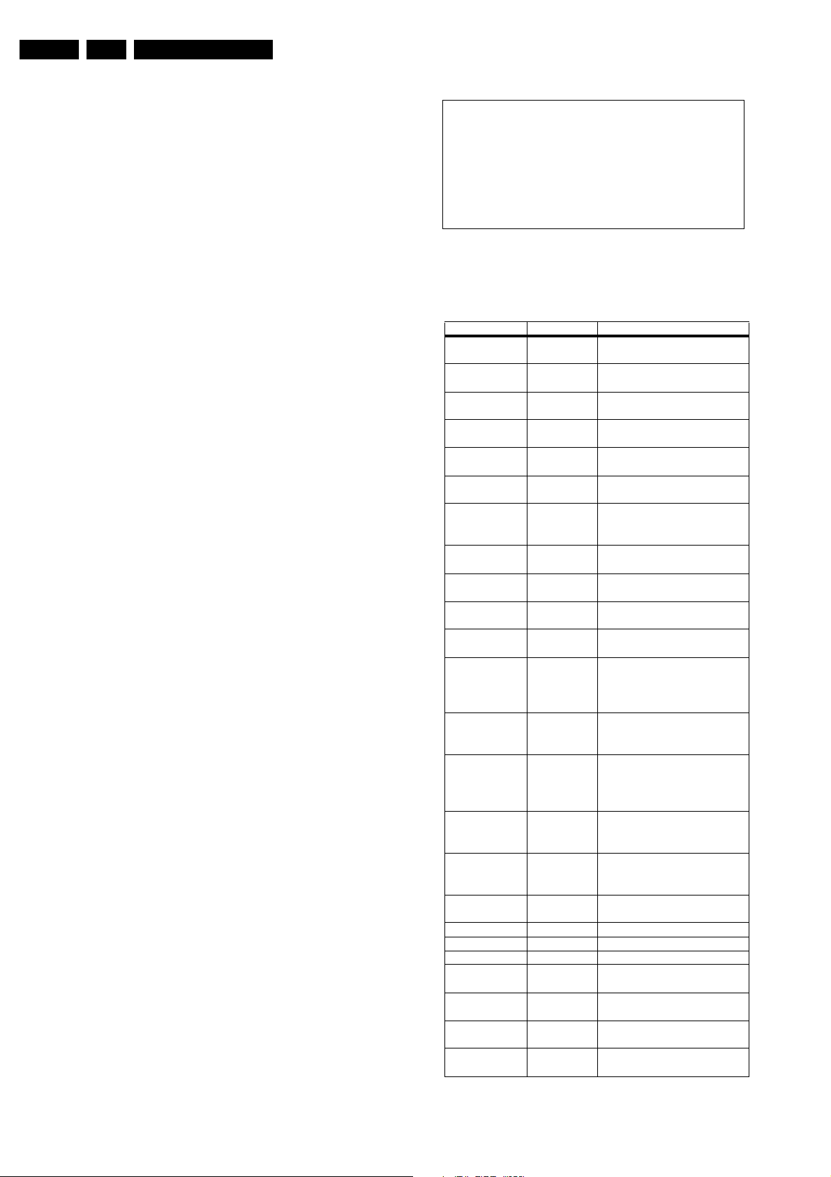
4.3 Service Positions
This chassis has several predefined service positions, for
better accessibility. They are explained below in more detail.
4.3.1 Solder Side '3rd SCART' panel
2
1
4
4
4.2.2 Rear Cover Removal
1
1
3
SERVICE CONNECTOR
2
Figure 4-1 Rear view
Warning: disconnect the mains power cord before you remove
the rear cover.
First, remove the top cover (= plate with 'saucer'):
1. Remove the fixation screw(s) [1] that hold the cover plate.
2. Pull the cover (horizontally) backwards.
To be able to access the electronics of the set, you must
remove the rear cover:
1. Remove the fixation screws [2] of the rear I/O cover plate.
2. Remove the remaining fixation screws [3] at the two sides,
and at the top of the rear cover.
3. Release at bottom side the rear cover securing clips and
remove the rear cover. Make sure that wires and cables will
not be damaged during the cover remove action.
1
CL 36532017_041.eps
110403
3
1680
CL 16532044_010.eps
140501
Figure 4-2 Service position 1
3
To remove or access the '3rd SCART' panel, do the following:
1. Remove fixation screw [1].
2. To release the fixation peg, push it towards the CRT [2].
3. At the same time, pull the complete module away from the
LSP [3]. It hinges in the LSP-bracket. It is also possible to
uncouple both hinges.
4. To remove the panel, disconnect the flat-cable from
connector 1680 and remove the four panel screws [4].
4.3.2 Double Window PIP panel (If present)
1. Release the securing clamps and take out of the PWB to
service the Double window PWB.
EN 18 EM5.1E4.
Mechanical Instructions
4.3.3 Component Side LSP
SSB top-bracket
SSB
AUTO-SCAVEM
bracket
CONNECTOR SUPPORT
bracket
Bottom tray
2
LOT - bracket
LSP
1
1
2
Figure 4-3 Service position 2
For better accessibility of the LSP, do the following (see figure
above):
1. Remove the LSP-bracket from the bottom tray by pulling it
backwards.
2. Hook the bracket in the first row of fixation holes of the
bottom tray. In other words, reposition the bracket from [1]
to [2].
4.3.4 Solder Side LSP
2
CL 26532041_065.eps
110402
To get access to the bottom side (solder side) of the LSP, do
the following (see figure above):
1. Unlock the DAF-module bracket (see paragraph 'DAF
Assy/Panel' further down).
2. Unlock the Double Window, PIP module (if present),
release the locking clip and pull the bracket out of the
locking holes in the bottom plate.
3. Disconnect the degaussing coil connector 1502 [1] from
the LSP.
4. Release the high voltage cable out of its guiding clamp.
5. Release the wiring from their fixation clamps, in order to
position the LSP in the service position.
6. Some cables should be led underneath the CRT panel
instead of above this panel.
7. Move the LSP to the left, at the same time rotate the panel
90 degrees clockwise [2] and next, place it upright at the
left side of the bottom tray [3].
8. Put the panel with the right sided locking hook in the
oblique accessed mounting hole in the bottom plate and
pull it backwards to lock the panel in this position.
4.3.5 Small Signal Board (SSB)
Caution:
Always switch the set completely ‘OFF’ (disconnect the mains
cord) before you remove or replace the SBB.
As the 5V2 standby voltage is always present (while the set is
switched ‘On’, in ‘Standby’ or in ‘Protection’ mode) on the
SIMM connector, it is very risky to remove the SSB in this
situation, because the risk of short circuiting is very great.
In fact, there is no predefined service position for the SSB. Most
test points are located on the A-side (side that is facing the
tuner). If you have to replace ICs, you must take the complete
SSB module out of the SIMM-connector.
Note: For good access to the A-side, it is necessary to remove
the Auto-Scavem assy (at the left side of the SSB). See
description in paragraph ‘Assy/Panel removal' to remove the
Auto-Scavem panel/bracket.
To get access to the SSB test points, do the following:
1
1502
1
2
CL 26532041_067.eps
110402
Figure 4-5 SSB removal (part 1)
1. Put the LSP in service position 2 (as described above).
2. Release the two clamps at the top of the SSB bracket [2]
and pull the bracket upward (it hinges in the bracket at the
3
LOT side).
3. Now you can remove the complete SSB bracket.
CL 26532041_066.eps
110402
Figure 4-4 Service position 3
1
SSB
Mechanical Instructions
EN 19EM5.1E 4.
4.4 Assy / Board Removal
3
Sometimes, it can be necessary to swap a complete assy or
Printed Wiring Board (PWB). How that can be done is
explained below.
4.4.1 Top Control Assy/Panel
2
2
CL 26532041_068.eps
110402
Figure 4-6 SSB removal (part 2)
1. Push the top of the SSB towards the LOT [1].
2. Due to the pressure, the two metal clamps at both sides of
the SIMM-connector will release [2].
3. Take the complete SSB out [3].
SAM
SDM
2
Top control board
Figure 4-8 Top control assy
1. Release both fixation screws about 5 full turns.
2. Pull the complete assy back- and upwards (it hinges in the
cabinet front).
3. Flip the assy, and you can access the board by releasing
(carefully) the four fixation clamps.
4.4.2 Side-I/O Assy and Panel
3
2
2
1
CL 16532149_068.eps
051201
SSB
1
1
Figure 4-7 SSB removal (part 3)
1. Once you have taken out the SSB, remove the shieldings
[2]. Sometimes it is necessary to unsolder some soldertags first [1].
2. Now re-place the SSB module in the SIMM-connector in
reverse order.
Notes:
For better access to the SSB, it is possible to order an
'extension tool' with cables. You can use this service extension
tool to connect a Small Signal Board (SSB) of an A10 or EMG
(EMx) chassis, via 2 “IDE” cables to the SIMM connector in the
set. In this way, you can service the SSB more easily outside
the TV set. You can order this tool under 12nc: 9965 000
14526.
CL 26532041_069.eps
110402
Figure 4-9 Side I/O assy
1. Release the snap-hook [1] with your finger.
2. At the same time, pull the assy backwards [2].
3. Release the two fixation clamps on the right side of the
bracket (the I/O board hinges at the left side).
4. Remove the board from the bracket.
4.4.3 Mains Switch Assy/Panel
1
1
2
Figure 4-10 Mains Switch Assy
CL 16532149_069.eps
061201
CL 16532149_070.eps
061201

EN 20 EM5.1E4.
Mechanical Instructions
1. Release the two fixation clamps (rather difficult to reach),
by pushing them upwards [1]. At the same time, pull the
complete assy backwards [2].
Note: be aware that the degaussing coil can hamper this.
2. Release the two fixation clamps on the two sides of the
bracket (the board hinges at the connector side).
3. Remove the board from the bracket.
4. When the light guide (sitting in the cabinet, in front of the
LEDs) is defective, you can replace it by pushing it
forwards at the left side (it hinges at the right side, seen
from the rear).
4.4.4 DAF Assy/Panel
1
2
4
4
3
3
CL 16532044_011.eps
4.4.8 Large Signal Panel (LSP)
1. Remove the SSB (see paragraph 'Small Signal Board,SSB'
above).
2. Remove the Auto-Scavem assy (see paragraph 'Auto
Scavem Assy/Panel' above).
3. Disconnect the necessary cables.
4. Release the fixation clamps on the left of the LSP-bracket
(the board hinges at the right side).
5. Remove the board from the bracket.
4.5 Set Re-assembly
To reassemble the whole set, do all processes in reverse order.
Be sure that, before the rear cover is mounted:
• The mains cord is mounted correctly in its guiding brackets.
• All wires/cables are returned in their original positions. This
is very important due to the large 'hot' area of the set
150501
Figure 4-11 DAF-module
1. Remove the fixation screw [1] (if present).
2. Push down the fixation clamp [2], and pull the complete
bracket at the same time away from the CRT [3]. The
module is now free from the LSP-bracket.
3. Release the fixation clamps [4], in order to remove the print
from its bracket.
4.4.5 Double window, PIP panel (If present)
1. It is not necessary to remove the Double window bracket.
2. To remove he Double window PWB, release both upper
clamps and take out the PWB.
4.4.6 Auto-SCAVEM Assy/Panel
This panel is placed on the left side of the SSB (See figure
'Service Position 2'). Because most of its components are
placed on the bottom side, you must lift the panel from its
bracket before you can measure it.
1. Therefore, release the two fixation clamps at the top side.
2. Lift the panel from the bracket (it hinges at the bottom).
To remove the bracket:
1. First, remove the panel from the bracket, as described
above.
2. Then, remove the two fixation screws at the bottom.
3. Lift the Auto-Scavem bracket slightly up, and at the same
time bend the top a little away from the tuner.
4. Now, push the bracket into the direction of the CRT, and lift
it out of the LSP-bracket.
4.4.7 Small Signal Board (SSB)
See paragraph 'Small Signal Board (SSB)' above.

Service Modes, Error Codes, and Fault Finding
5. Service Modes, Error Codes, and Fault Finding
EN 21EM5.1E 5.
Index of this chapter:
1. Test points
2. Service Modes
3. Problems and solving tips (related to CSM)
4. ComPair
5. Error Codes
6. The blinking LED procedure
7. Protections
8. Repair tips
5.1 Test Points
The chassis is equipped with test points printed on the circuit
board assemblies. They refer to the diagram letters.
Perform measurements under the following conditions:
• Service Default Mode.
• Video: colour bar signal.
• Audio: 3 kHz left, 1 kHz right.
5.2 Service Modes
Service Default Mode (SDM) and Service Alignment Mode
(SAM) offer several features for the service technician, while
the Customer Service Mode (CSM) is used for communication
between a Philips Customer Care Centre (P3C) and a
customer.
There is also the option of using ComPair, a hardware interface
between a computer (see requirements below) and the TV
chassis. It offers the ability of structured troubleshooting, test
pattern generation, error code reading, software version
readout, and software upgrading.
Minimum requirements: a Pentium processor, Windows 95/
98, and a CD-ROM drive (see also paragraph "ComPair").
Note: In this chassis, two LED configuration are possible: with
bicoloured LED (red/green) or with separate blue and red
LEDs. The bicoloured version is the one we know from EM5E.
The version with blue LED works slightly different. The blue
LED is controlled by software (via ON_OFF_LED). The red
LED will light in anti-phase to the blue one, but with a time
delay. This means that if the blue LED is blinking fast, the red
LED will stay off. But after the blue LED is "OFF" long enough,
the red LED will go "ON".
So take care: In certain service modes (e.g. blinking LED,
stepwise start-up, etc.) you must observe the blue LED and
ignore the red LED.
5.2.1 Service Default Mode (SDM)
Purpose
• To create a pre-defined setting, to get the same
measurement results as given in this manual.
• To override SW protections.
• To start the blinking LED procedure.
Specifications
• Tuning frequency: 475.25 MHz for PAL/SECAM.
• Colour system: SECAM L for France or PAL B/G for the
rest of Europe.
• All picture settings at 50 % (brightness, colour, contrast).
• All sound settings at 50 %, except volume at 25 %.
• All service-unfriendly modes (if present) are disabled, like:
– (Sleep) timer.
– Child/parental lock.
– Blue mute.
– Automatic volume limiter (AVL).
– Auto switch-off (when no video signal was received for
10 minutes).
– Skip/blank of non-favourite pre-sets.
– Smart modes.
– Auto store of personal presets.
– Auto user menu time-out.
How to enter SDM
Use one of the following methods:
• Use the standard RC-transmitter and key in the code
"062596", directly followed by the "MENU" button.
Note: It is possible that, together with the SDM, the main
menu will appear. To switch it off, push the "MENU" button
again.
• When you shorten for a moment the two solder pads on the
'external part' of the SSB print, with the indication "SDM".
Activation can be performed in all modes, except when the
set has a problem with the main-processor.
Caution: If the SDM is entered via the pins, all the
software-controlled protections are de-activated.
• Use the DST-emulation feature of ComPair.
• Use the "DEFAULT" button on the Dealer Service Tool
(RC7150).
After entering this mode, "SDM" will appear in the upper right
corner of the screen.
How to navigate
When you press the "MENU" button on the RC transmitter, the
set will toggle between the SDM and the normal user menu
(with the SDM mode still active in the background).
How to exit SDM
Use one of the following methods:
• Switch the set to STANDBY via the RC-transmitter.
• Press the "EXIT" button on the DST.
• Via a standard customer RC-transmitter: key in "00"-
sequence.
5.2.2 Service Alignment Mode (SAM)
Purpose
• To perform (software) alignments.
• To change option settings.
• To easily identify the used software version.
• To view operation hours.
• To display (or clear) the error code buffer.
Specifications
• Operation hours counter.
• Software version.
• Option settings.
• Error buffer reading and erasing.
• Software alignments.
How to enter SAM
Use one of the following methods:
• Via a standard RC transmitter: key in the code "062596"
directly followed by the "OSD [i+]" button. After activating
SAM with this method a service warning will appear on the
screen, you can continue by pressing any digit key on the
RC.
• Short for a moment the two solder pads on the 'external
part' of the SSB print, with the indication SAM. Depending
on the software version it is possible that the service
warning will appear, you can continue by pressing any digit
key on the RC.
• Use the DST-emulation feature of ComPair.
• Press the ALIGN button on the DST while the set is in the
normal operation
EN 22 EM5.1E5.
Service Modes, Error Codes, and Fault Finding
After entering this mode, "SAM" will appear in the upper right
corner of the screen.
Contents of SAM:
• OPERATION HOURS. Displays the accumulated total of
operation hours (not the standby hours).
• HARDWARE INFO
– ROM VERSION. Displays the date of the software and
the software version of the ROM (example: EM51EU1-
1.0_01234 = AAABBC-X.Y_NNNNN).
• AAA= the chassis name.
• BB= the region: EU= Europe, AP= Asia Pacific
PAL/Multi, AN= Asia Pacific NTSC, US= USA, LT=
LATAM.
• C= the language cluster number.
• X.Y= the software version, where X is the main
version number (different numbers are not
compatible with one another) and Y is the sub
version number (a higher number is always
compatible with a lower number).
• NNNNN= last five digits of 12nc code software.
• ERRORS (followed by maximal 10 errors). The most
recent error is displayed at the upper left (for an error
explanation see paragraph "Error Codes").
• DEFECTIVE MODULE. Here the module that generates
the error is displayed. If there are multiple errors in the
buffer, which are not all generated by a single module,
there is probably another defect. It will then display the
message "UNKNOWN" here.
• RESET ERROR BUFFER. When you press the "OK"
button, the error buffer is reset.
• ALIGNMENTS. This will activate the "ALIGNMENTS" sub-
menu.
• DEALER OPTIONS. Extra features for the dealers.
• SERVICE OPTIONS. Extra features for Service.
• INITIALISE NVM. When an NVM was corrupted (or
replaced) in the former EM3 chassis, the microprocessor
replaces the content with default data (to assure that the
set can operate). However, all pre-sets and alignment
values are gone now, and option numbers are not correct.
Therefore, this was a very drastic way. In this chassis, the
procedure is implemented in another way: The moment the
processor recognises a corrupted NVM, the "INITIALISE
NVM" line will be highlighted. Now, you can do two things
(dependent of the service instructions at that moment):
– Save the content of the NVM via ComPair for
development analysis, before initialising. This will give
the Philips Service department an extra possibility for
diagnosis (e.g. when Development asks for this).
– Initialise the NVM (same as in the past, however now it
happens conscious).
• STORE. All options and alignments are stored when
pressing the "OK"-button
• FUNCTIONAL TEST. All devices are tested via the "OK"
button. Eventual errors are displayed in the error buffer.
The error buffer is not erased, the content returns when this
test is terminated.
• DAILY MENUS. With the "OK" button, you can go to the
normal user menu. SAM is still active in the background.
With the "MENU" button, you return from the user menu to
SAM menu. This feature can be helpful to quickly change
some settings in the user menu.
• SW MAINTENANCE
– UPGRADE. Not applicable for this chassis
– EVENTS. Not useful for service purposes. In case of
specific software problems, the development
department can ask for this info.
– BDM INFO. Broadcast Debug Menu info. The purpose
of this menu is to debug the broadcast, NOT the TV.
The menu gives an overview of what is received on the
current preset. Following items are displayed:
P r e s e t n r : -- UTC: - - : - - : --
P r e s e t n a m e : ----- LTO: - - : - - : --
Time: - - : - - : --
C N I N V M : ---- Date: - - / - - / ----
C N I F 1 : ----
C N I F 2 : ---- Time TXT: - - : - - : --
C N I V P S : ---- Time 8/30 F1: - - : - - : --
M o r n i n g P r o g : --- Date 8/30 F1: - - / - - / ----
N a m e 8 / 3 0 F 1 : ----- LTO 8/30 F1: - - : - - : --
N a m e 8 / 3 0 F 2 : -----
N a m e T X T : ----- WSS G1: - - - -
S i g n a l S t r e n g t h :--- WSS G2: - - - -
WSS G3: - - -
E P G S e r v i c e : --- WSS G4: - - -
CL 36532017_055.eps
240403
Figure 5-1 Broadcast debug menu overview
Table 5-1 Broadcast debug menu explanation
Item Source Description
Presetnr Set Presetnumber of the current
selected preset.
Presetname Set Presetname of the current se-
lected preset.
CNI NVM Broadcaster CNI number stored in NVM
for the current preset.
CNI F1 Broadcaster CNI number from transmitted
Packet 8/30 Format 1.
CNI F2 Broadcaster CNI number from transmitted
Packet 8/30 Format 2.
CNI VPS Broadcaster CNI number from transmitted
VPS line.
Morning Prog Broadcaster "ARD" or "ZDF" according to
dedicated bit in 8/30 Format
1.
Name 8/30 F1 Broadcaster Name extracted from status
message of 8/30 Format 1.
Name 8/30 F2 Broadcaster Name extracted from status
message of 8/30 Format 2.
Name TXT Broadcaster Name extracted from TXT
header.
Signal Strength FBX Noise figure measured for se-
lected preset.
EPG Service Set EPG Service stored in NVM
for current preset displayed
as "TXT", "MCP", "SCP",
"OCP".
UTC Set UTC (Universal Time Code
formerly known as Greenwich
Mean Time) used in the set.
LTO Set LTO (Local Time Offset) used
in the set. Used by EPG for
all Nextview displays. (= Time
TXT header - Time 8/30 F1 )
Time Set Current time running in the
set. Was extracted at startup,
then maintained by software.
Date Set Current date running in the
set. Was extracted at startup,
then maintained by software.
Time TXT Broadcaster TXT header time from the se-
lected preset.
Time 8/30 F1 Broadcaster UTC time from 8/30 Format 1.
Date 8/30 F1 Broadcaster Date from 8/30 Format 1.
LTO 8/30 F1 Broadcaster LTO from 8/30 Format 1.
WSS G1 Broadcaster WSS Group 1 (Aspect Ratio)
bits 0 1 2 3
WSS G2 Broadcaster WSS Group 2 (Enhanced
Services) bits 4 5 6 7
WSS G3 Broadcaster WSS Group 3 (Subtitles) bits
8 9 10
WSS G4 Broadcaster WSS Group 4 (Reserved) bits
11 12 13

Service Modes, Error Codes, and Fault Finding
EN 23EM5.1E 5.
How to navigate
• In SAM, you can select the menu items with the "CURSOR
UP/DOWN" key on the RC-transmitter. The selected item
will be highlighted. When not all menu items fit on the
screen, move the "CURSOR UP/DOWN" key to display the
next/previous menu items.
• With the "CURSOR LEFT/RIGHT" keys, it is possible to:
– (De) activate the selected menu item.
– Change the value of the selected menu item.
– Activate the selected submenu.
How to exit SAM
Use one of the following methods:
• Press the "MENU" button on the RC-transmitter, or
• Switch the set to STANDBY via the RC-transmitter, or
• Press the "EXIT" button on the DST.
5.2.3 Customer Service Mode (CSM)
Purpose
When a customer is having problems with his TV-set, he can
call his dealer. The service technician can than ask the
customer to activate the CSM, in order to identify the status of
the set. Now, the service technician can judge the severity of
the complaint. In many cases, he can advise the customer how
to solve the problem, or he can decide if it is necessary to visit
the customer.
The CSM is a read only mode; therefore, modifications in this
mode are not possible.
How to enter CSM
Use one of the following methods:
• Press the "MUTE" button on the RC-transmitter
simultaneously with the "MENU" button on the TV (top
control) for at least 4 seconds.
• Key in the code "123654" via the standard RC transmitter.
Note: Activation of the CSM is only possible if there is no (user)
menu on the screen!
How to navigate
By means of the "CURSOR-DOWN/UP" knob on the RCtransmitter, you can navigate through the five menus.
Contents of CSM
Customer Service Menu 1
• SOFTWARE VERSION (example: EM51EU1-
1.0_01234). Displays the build in software version. In case
of field problems related to software, software flash-RAM
pos.7006 must be changed by a new one. Do this via
soldering. You will find details of the software versions in
the chapter "Software Survey" of the "Product Survey Colour Television" publication. This publication is
generated four times a year.
• FEATURE BOX. The 12NC-number of the build in Feature
Box software
• SET TYPE. This information is very helpful for a helpdesk/
workshop as reference for further diagnosis. In this way, it
is not necessary for the customer to look at the rear of the
TV-set.
• CODE 1. Gives the latest 5 errors of the error buffer. As
soon as the built-in diagnose software has detected an
error the buffer is adapted. The last occurred error is
displayed on the leftmost position. Each error code is
displayed as a 3-digit number. When less than 10 errors
occur, the rest of the buffer is empty (000). See also
paragraph "Error Codes" for a description.
• CODE 2. Gives the first 5 errors of the error buffer. See
also paragraph Error Codes for a description.
• VOLUME. Gives the last status of the volume as set by the
customer. The value can vary from 0 (volume is minimum)
to 100 (volume is maximum). Volume values can be
changed via the volume key on the RC-transmitter.
• BRIGHTNESS. Gives the last status of the brightness as
set by the customer. The value can vary from 0 (brightness
is minimum) to 100 (brightness is maximum). Brightness
values can be changed via the "CURSOR LEFT" and
"CURSOR RIGHT" keys on the RC-transmitter after
pressing the "MENU" button and selecting "PICTURE" and
"BRIGHTNESS".
• CONTRAST. Gives the last status of the contrast as set by
the customer. The value can vary from 0 (contrast is
minimum) to 100 (contrast is maximum). Contrast values
can be changed via "CURSOR LEFT" and "CURSOR
RIGHT" keys on the RC-transmitter after pressing the
"MENU" button and selecting "PICTURE" and
"CONTRAST".
• COLOUR. Gives the last status of the colour saturation, as
set by the customer. The value can vary from 0 (colour is
minimum) to 100 (colour is maximum). Colour values can
be changed via "CURSOR LEFT" and "CURSOR RIGHT"
keys on the RC-transmitter after pressing the "MENU"
button and selecting "PICTURE" and "COLOUR".
• HUE. Only relevant for NTSC-signals (e.g. some NTSC-
DVD-discs).
Customer Service Menu 2
• SHARPNESS. Gives the sharpness value. The value can
vary from 0 (sharpness is minimum) to 7 (sharpness is
maximum). In case of bad antenna signals, a too high
value of the sharpness can result in a noisy picture.
Sharpness values can be changed via the "CURSOR
LEFT" and "CURSOR RIGHT" keys on the RC-transmitter
after pressing the "MENU" button and selecting
"PICTURE" and "SHARPNESS".
• HEADPHONE VOLUME. Gives the last status of the
headphone volume, as set by the customer. The value can
vary from 0 (volume is minimum) to 100 (volume is
maximum). Headphone volume values can be changed via
the "CURSOR LEFT" and "CURSOR RIGHT" keys on the
RC-transmitter after pressing the "MENU" button and
selecting "SOUND" and "HEADPHONE VOLUME".
• DOLBY. Indicates whether the received transmitter
transmits Dolby sound ("ON") or not ("OFF"). Attention:
The presence of Dolby can only be tested by the software
on the Dolby Signalling bit. If a Dolby transmission is
received without a Dolby Signalling bit, this indicator will
show "OFF" even though a Dolby transmission is received.
• SURROUND MODE. Indicates the by the customer
selected surround mode (or automatically chosen mode).
In case the set is a Non-Dolby set, there will be displayed
"0". If it is a Dolby-set then is displayed: "STEREO", "3
STEREO", "HALL", "3DSURROUND", "DOLBY PRO
LOGIC" or "DOLBY DIGITAL". These settings can be
influenced after pressing the "MENU" button and selecting
"SOUND" and SURROUND MODE". It can also have been
selected automatically by signalling bits (internal software).
• TUNER FREQUENCY. Indicates the frequency the
selected transmitter is tuned to. The tuner frequency can
be changed via the "CURSOR LEFT" and "CURSOR
RIGHT" keys for fine tune after opening the installation
menu and selecting "INSTALL" and "MANUAL INSTALL".
• DIGITAL OPTION. Gives the selected digital mode, "100
HZ", "DIGITAL SCAN", "NATURAL MOTION", "DOUBLE
LINES", or "PIXEL PLUS". Change via "MENU",
"PICTURE", "DIGITAL OPTIONS".
• CENTRE TRIM. Indicates the difference between main
volume and volume of centre speaker. Change via:
"MENU", "SETUP", "SPEAKERS", and "CENTRE
VOLUME" (not available when "Surround Mode" is set to
"STEREO" or "HALL"). The value can vary from "-10" to
"+10"
• TV SYSTEM. Gives information about the video system of
the selected transmitter.
– BG: PAL BG signal received.
– DK: PAL DK signal received.

EN 24 EM5.1E5.
Service Modes, Error Codes, and Fault Finding
– I: PAL I signal received.
– L/La: SECAM L/La signals received.
– M: NTSC M signal received with video carrier on 38.9
MHz.
Customer Service Menu 3
• BALANCE. Indicates the balance settings, between "-50"
and "+50". Change via "MENU", "SOUND", and
"BALANCE". Not applicable for Dolby Pro Logic sets.
• CENTRE MODE. Indicates if centre mode is set "ON" or
"OFF". When centre mode is on, all TV speakers are used
as one centre speaker. Change Centre mode via "MENU",
"SETUP", "SPEAKERS", and "CENTRE MODE".
• DNR. Gives the selected DNR setting (Dynamic Noise
Reduction), "OFF", "MINIMUM", "MEDIUM", or
"MAXIMUM". Change via "MENU", "PICTURE", "DNR"
• NOISE FIGURE. Gives the noise ratio for the selected
transmitter. This value can vary from 0 (good signal) to 127
(average signal) and to 255 (bad signal). For some
software versions, the noise figure will only be valid when
"Active Control" is set to "medium" or "maximum".
• SOURCE. Indicates which source is used and the video/
audio signal quality of the selected source. (Example:
Tuner, Video/NICAM) Source: "TUNER", "EXT1", "EXT2",
"EXT3", "EXT4", "SIDE", "AV1", "AV2", "AV3" or "AV4".
Video signal quality: "VIDEO", "S-VIDEO", "RGB 1FH",
"YPBPR 1FH 480P", "YPBPR 1FH 576P", "YPBPR 1FH
1080I", "YPBPR 2FH 480P", "YPBPR 2FH 576P", "YPBPR
2FH 1080I", "RGB 2FH 480P", "RGB 2FH 576P" or "RGB
2FH 1080I". Audio signal quality: "STEREO", "SPDIF 1",
"SPDIF 2" or "SPDIF".
• AUDIO SYSTEM. Gives information about the audio
system of the selected transmitter: "ANALOGUE MONO",
"ANALOGUE STEREO", "PCM 2/0", "DD 1/0", "DD 2/0
LtRt", "DD 2/0 L0R0", "DD 2/1", "DD 2/2", "DD 3/0", "DD 3/
1", "DD 3/2", "DD 1+1", "MPEG 1/0", "MPEG 2/0", "MPEG
2/0 LtRt", "MPEG 2/1", "MPEG 2/2", "MPEG 3/0", "MPEG
3/1", "MPEG 3/2", "MPEG 1+1" or "MPEG 2+2".
• TUNED BIT. Gives information about the tuning method of
the stored pre-set. If a channel is found via "automatic
installation", you will see the value "Off". When you change
this (automatically found) frequency via "fine tune"
adjustment (installation menu - manual installation), the
displayed value will change to "On". Therefore, when you
see the value "On" in this line, it is an indication that the
received channel is a non-standard signal (e.g. of a VCR).
• SURROUND SPEAKERS. Indicates if the surround
speakers are present, "YES" or "NO". Change via "MENU",
"SETUP", "SPEAKERS", and "SURROUND SPEAKERS".
• ON TIMER. Indicates if the "On Timer" is set "ON" or "OFF"
and if the timer is "ON" also displays start time, start day
and program number. Change via "MENU", "TV",
"FEATURES", and "ON TIMER".
• PRESET LOCK. Indicates if the selected preset has a child
lock: "LOCKED" or "UNLOCKED". Change via "MENU",
"TV", "FEATURES", "CHILD LOCK", and "CUSTOM
LOCK".
"CUSTOM LOCK". It is possible that more than one value
is shown.
• PROGRAM CATEGORY. Indicates the theme of the
selected transmitter: "MOVIES", "NEWS", "SHOWS",
"SPORTS", "CHILDREN", "MUSIC", "CULTURE", or
"SERIES".
• TV RATINGS LOCK. Only applicable for US.
• MOVIE RATINGS LOCK. Only applicable for US.
• V-CHIP TV STATUS. Only applicable for US.
Customer Service Menu 5
• V-CHIP MOVIE STATUS. Only applicable for US.
• OPTIONS 1. Gives the option codes of option group 1 as
set in SAM (Service Alignment Mode).
• OPTIONS 2. Gives the option codes of option group 2 as
set in SAM (Service Alignment Mode).
• AVL. Indicates the last status of AVL (Automatic Volume
Level): "ON" or "OFF". Change via "MENU", "TV",
"SOUND", "AVL"
• DELTA VOLUME. Indicates the last status of the delta
volume for the selected preset as set by the customer: from
"-12" to "+12". Change via "MENU", "TV", "SOUND",
"DELTA VOLUME".
• SURROUND TRIM L. Indicates the last status of
"SURROUND LEFT VOLUME" as set by the customer:
from "-10" to "+10". Only available in Digital Dolby sets.
Change via "MENU", "SETUP", "SPEAKERS",
"SURROUND L VOLUME.
• SURROUND TRIM R. Indicates the last status of
"Surround Right Volume" as set by the customer: from "10" to "+10". Only available in Digital Dolby sets. Change
via "MENU", "SETUP", "SPEAKERS", "SURROUND R
VOLUME.
• FRONT SPKR DIST. Indicates the last status of the
distance to the front speakers as set by the customer: "1m",
"2m", or "3m",.... Change via "MENU", "SETUP",
"SPEAKERS", "TO FRONT".
• SURR. SPKR DIST. Indicates the last status of the
distance to the surround speakers as set by the customer:
"1m", "2m", or "3m",.... Change via "MENU", "SETUP",
"SPEAKERS", "TO SURROUND".
How to exit CSM
Use one of the following methods:
• After you press a key on the RC-transmitter (with exception
of the "CHANNEL", "VOLUME" and digit (0-9) keys), or
• After you switch the TV-set "OFF" with the mains switch.
5.3 Problems and Solving Tips (related to CSM)
Note: Below described problems are all related to the TV
settings. The procedures to change the value (or status) of the
different settings are described above. New value(s) are
automatically stored.
5.3.1 Picture Problems
Customer Service Menu 4
• CHILD LOCK. Indicates the last status of the general child
lock: "UNLOCK", "LOCK", or "CUSTOM LOCK". Change
via "MENU", "TV", "FEATURES", "CHILD LOCK", and
"LOCK".
• AGE LOCK. Indicates the last status of the EPG rating for
child lock: "OFF", "4 YEARS", "6 YEARS", "8 YEARS", "10
YEARS", "12 YEARS", "14 YEARS" or "16 YEARS". This
is only displayed if child lock is set to "CUSTOM LOCK"
• LOCK AFTER. Indicates at what time the child lock is set:
"OFF" or e.g. "18:45" (lock time). This is only displayed if
child lock is set to "CUSTOM LOCK"
• CATEGORY LOCK. Indicates the last status of the EPG
theme childlock: "MOVIES", "NEWS", "SHOWS",
"SPORTS", "CHILDREN", "MUSIC", "CULTURE", or
"SERIES". This is only displayed if child lock is set to
Snowy/noisy picture
1. Check line 24 "Noise Figure". In case the value is 127 or
higher, and the value is also high on other programs, check
the aerial cable/aerial system. For some software
versions, the noise figure will only be valid when "Active
Control" is set to "medium" or "maximum".
2. Check lines 11 "Sharpness" and 24 "Noise Figure". In case
the value of line 11 is 3 or 4 and the value of line 24 is high
(127 or higher), decrease the "Sharpness" value.
Picture too dark
1. Press "MENU", "TV", "PICTURE", "SMART PICTURE". In
case the picture improves, increase the "Brightness" or the
"Contrast" value. The new value(s) are automatically
stored (in "personal" pre-set) for all TV channels.

Service Modes, Error Codes, and Fault Finding
EN 25EM5.1E 5.
2. Check line 7 "Brightness" and 8 "Contrast". If the value of
line 7 is low (< 10) or the value of line 8 is low (< 10),
increase the "Brightness" or the "Contrast" value.
Picture too bright
1. Press "MENU", "TV", "PICTURE", "SMART PICTURE". In
case the picture improves, decrease the "Brightness" or
the "Contrast" value. The new value(s) are automatically
stored (in "personal" pre-set) for all TV channels.
2. Check lines 7 "Brightness" and 8 "Contrast". If the value of
line 7 is high (> 40) or the value of line 8 is high (> 50).
Decrease the "Brightness" value or increase the "Contrast"
value.
White line around picture elements and text
1. Press "MENU", "TV", "PICTURE", "SMART PICTURE". In
case the picture improves, decrease the "Sharpness"
value. The new value is automatically stored (in "personal"
pre-set) for all TV channels.
2. Check line 11 "Sharpness". Decrease the "Sharpness"
value. The new value is automatically stored for all TV
channels.
No picture
Check line 27 "Tuned bit". In case the value is "No", install the
required program again. Open the installation menu and
perform manual installation.
Blue picture
No proper signal is received. Check the aerial cable/aerial
system.
Blue picture and/or unstable picture
A scrambled or decoded signal is received.
Black and white picture
Check line 9 "Colour". In case the value is low (< 10), increase
the "Colour" value. The new value is automatically stored for all
TV channels.
No colours/colour lines around picture elements or colours not correct or unstable picture
1. Check line 20 "TV System". If a "strange" system pops up,
something has gone wrong during installation. Re-install
the channel.
2. In case line 20 is "L", the installed system for this pre-set is
"France", while "West Europe" is required. Install the
required program again: open the installation menu and
perform manual installation. Select system "West Europe".
Menu text not sharp enough
1. Press "MENU", "TV", "PICTURE", "SMART PICTURE". In
case picture improves, decrease the contrast value. The
new value(s) are automatically stored for all TV channels.
2. Check line 8 "Contrast". The value of line 8 is high (> 50).
Decrease the contrast value.
5.3.2 Sound Problems
No sound from left and right speaker
Check line 6 "Volume". The value is low. Increase the value of
"Volume". The new value(s) are automatically stored (in
"personal" pre-set) for all TV channels.
Sound too loud for left and right speaker
Check line 6 "Volume". The value is high. Decrease the value
of " Volume". The new value(s) are automatically stored (in
"personal" pre-set) for all TV channels.
5.4 ComPair
5.4.1 Introduction
ComPair (Computer Aided Repair) is a service tool for Philips
Consumer Electronics products. ComPair is a further
development on the European DST (service remote control),
which allows faster and more accurate diagnostics. ComPair
has three big advantages:
• ComPair helps you to quickly get an understanding on how
to repair the chassis in a short time by guiding you
systematically through the repair procedures.
• ComPair allows very detailed diagnostics (on I2C level)
and is therefore capable of accurately indicating problem
areas. You do not have to know anything about I2C
commands yourself because ComPair takes care of this.
• ComPair speeds up the repair time since it can
automatically communicate with the chassis (when the
microprocessor is working) and all repair information is
directly available. When ComPair is installed together with
the SearchMan electronic manual of the defective chassis,
schematics and PWBs are only a mouse click away.
5.4.2 Specifications
ComPair consists of a Windows based faultfinding program
and an interface box between PC and the (defective) product.
The ComPair interface box is connected to the PC via a serial
or RS232 cable.
For this chassis, the ComPair interface box and the TV
communicate via a bi-directional service cable via the service
connector.
The ComPair faultfinding program is able to determine the
problem of the defective television. ComPair can gather
diagnostic information in two ways:
• Automatic (by communication with the television):
ComPair can automatically read out the contents of the
entire error buffer. Diagnosis is done on I2C level. ComPair
can access the I2C bus of the television. ComPair can
send and receive I2C commands to the micro controller of
the television. In this way, it is possible for ComPair to
communicate (read and write) to devices on the I2C
busses of the TV-set.
• Manually (by asking questions to you): Automatic
diagnosis is only possible if the micro controller of the
television is working correctly and only to a certain extends.
When this is not the case, ComPair will guide you through
the faultfinding tree by asking you questions (e.g. Does the
screen give a picture? Click on the correct answer: YES /
NO) and showing you examples (e.g. Measure test-point I7
and click on the correct oscillogram you see on the
oscilloscope). You can answer by clicking on a link (e.g.
text or a waveform picture) that will bring you to the next
step in the faultfinding process.
By a combination of automatic diagnostics and an interactive
question / answer procedure, ComPair will enable you to find
most problems in a fast and effective way.
Beside fault finding, ComPair provides some additional
features like:
• Up- or downloading of pre-sets.
• Managing of pre-set lists.
• Emulation of the Dealer Service Tool (DST).
• If both ComPair and SearchMan (Electronic Service
Manual) are installed, all the schematics and the PWBs of
the set are available by clicking on the appropriate
hyperlink.
Example: Measure the DC-voltage on capacitor C2568
(Schematic/Panel) at the Mono-carrier.
– Click on the "Panel" hyperlink to automatically show
the PWB with a highlighted capacitor C2568.
– Click on the "Schematic" hyperlink to automatically
show the position of the highlighted capacitor.
EN 26 EM5.1E5.
Service Modes, Error Codes, and Fault Finding
5.4.3 Stepwise Start-up
Under normal circumstances, a fault in the power supply, or an
error during start-up, will switch the television to protection
mode. ComPair can take over the initialisation of the television.
In this way, it is possible to distinguish which part of the startup routine (hence which circuitry) is causing the problem.
Take notice that the transition between two steps can take
some time, so give the set some time to reach a stable state.
During the transition time the LED can blink strangely.
Stepwise start- up explanation
This is realised via ComPair and is very helpful when a
protection is activated (see also chapter "Protections").
Table 5-2 Stepwise start-up table
State Description mode Display LED Enabled
0 Low power standby:
On None
5V2/3V3 present, uP in
standby-mode
1 High power Standby: TV-
set in standby-mode
2 Main Power On : HOP in
standby, 5V/8V present,
Wait 1s, flash
1 x
Wait 1s, flash
2 x
I2C protections on, SSB
is powered by standbysupply (5V/8V). Degaussing (12 s) has been
activated, MSP is reset.
3 Initialized (Semi stand-
by): most IC's are initial-
Wait 1s, flash
3 x
ized, HOP still in standby
4 HOP : HOP fully pow-
ered and working, EHT is
Wait 1s, flash
4 x
present, rest of IC's initialized, black current
stabilisation is off, picture
is still blanked
5 On: TV-set operates,
black current stabilisa-
Wait 1s, flash
5 x
tion is on, picture is unblanked
Note (*):
• When the set is in stepwise mode and, due to stepping-up,
a protection is activated, the set will really go into protection
(blinking LED). The set will not leave the stepwise-mode
however. If state X is the state where the set went to
protection, stepwise start-up will return to state X-1. At
state (X-1) diagnostic measurements can be performed.
Also, in the short time the set is in state X but not yet in
protection, you can also do some measurements.
5.4.4 How To Connect
1. First, install the ComPair Browser software (see the Quick
Reference Card for installation instructions).
2. Connect the RS232 interface cable between a free serial
(COM) port of your PC and the PC connector (marked with
"PC") of the ComPair interface.
3. Connect the mains adapter to the supply connector
(marked with "POWER 9V DC") of the ComPair interface.
4. Switch the ComPair interface "OFF".
5. Switch the television set "OFF" with the mains switch.
6. Connect the ComPair interface cable between the
connector on the rear side of the ComPair interface
(marked with "I2C") and the ComPair connector at the rear
side of the TV (situated just below the tuner input, see also
chapter 4).
protection
None
4 & 5
Plus 1, 6 &
18
Plus 2 & 16
7. Plug the mains adapter in a mains outlet, and switch the
interface "ON". The green and red LEDs light up together.
The red LED extinguishes after approx. 1 second while the
green LED remains lit.
8. Start the ComPair program and read the "Introduction"
chapter.
EXTERNAL 2
L
R
AUDIO EXTERNAL 1
SERVICE
CONNECTOR
PC VCR I2CPower
9V DC
Figure 5-2 ComPair Interface connection
5.4.5 How To Order
ComPair order codes (EU/AP):
• Starter kit ComPair32/SearchMan32 software and
ComPair interface (excl. transformer): 3122 785 90450.
• ComPair interface (excluding transformer): 4822 727
21631.
• Starter kit ComPair32 software (registration version): 3122
785 60040.
• Starter kit SearchMan32 software: 3122 785 60050.
• ComPair32 CD (update): 3122 785 60110.
• SearchMan32 CD (update): 3122 785 60120.
• ComPair interface cable: 3122 785 90004.
5.5 Error Codes
5.5.1 Introduction
The error code buffer contains all detected errors since the last
time the buffer was erased. The buffer is written from left to
right, new errors are logged at the left side, and all other errors
shift one position to the right.
When an error has occurred, the error is added to the list of
errors, provided the list is not full or the error is a protection
error.
When an error occurs and the error buffer is full, then the new
error is not added, and the error buffer stays intact (history is
maintained), except when the error is a protection error.
To prevent that an occasional error stays in the list forever, the
error is removed from the list after 50+ operation hours.
When multiple errors occur (errors occurred within a short time
span), there is a high probability that there is some relation
between them.
5.5.2 How to read the Error Buffer
Use one of the following methods:
• On screen via the SAM (only if you have a picture).
Examples:
– 0 0 0 0 0: No errors detected
– 6 0 0 0 0: Error code 6 is the last and only detected
error
– 9 6 0 0 0: Error code 6 was first detected and error
code 9 is the last detected error
• Via the blinking LED procedure (when you have no
picture). See next paragraph.
• Via ComPair.
CL96532156_029.eps
190600
Service Modes, Error Codes, and Fault Finding
EN 27EM5.1E 5.
5.5.3 How to clear the Error Buffer
Use one of the following methods:
• By activation of the "RESET ERROR BUFFER" command
in the SAM menu.
• With a normal RC, key in sequence "MUTE" followed by
"062599" and "OK".
• When you transmit the commands "DIAGNOSE" - "99" "OK" with ComPair (or with a DST).
• If the content of the error buffer has not changed for 50+
hours, it resets automatically.
5.5.4 Error Codes
In case of non-intermittent faults, clear the error buffer before
you begin the repair. This to ensure that old error codes are no
longer present. Before clearing the buffer, write down the
content, as this history can give you significant information.
Table 5-3 Error codes
Error Device Description Def. item Defect. module indi-
1 M24C32 NVM, spontaneous blinking error 1 7011 Control B5a
2 Hfail Protection Horizontal Flyback protection / Horizontal Flyback /
3 SAA4978 PICNIC 7713 Feature Box B3a
4 Supply 5V 5V protection / +5V Supply B5a
5 Supply 8V 8V protection / +8V Supply B5a
6 Slow I2C bus blocked Spontaneous blinking error 6 / Slow I2C Blocked /
7 TDA9330 HOP High-end Output Processor 7301 Video Controller B4
8 TDA932x HIP High-end Input Processor 7323 Chroma IF IO B2
9 PCF8574 Wireless expander 7501 Sound Output H
13 UV1318/... Tuner protection 1T01 Tuner A8
14 MSPxxxx ITT sound processor 7A02 Audio module B6a
16 FBX Feature Box Protection / +3V (Fbx) Supply B3
18 Fast I2C bus blocked Spontaneous blinking error 18 / Fast I2C Blocked /
19 TDA8444 Auto Scavem DAC 7500 Auto Scavem SC1
21 M62320P PIP I/O Expander 7403 Video Dual Screen C3
22 TDA888X PIP BOCMA 7301 Video Dual Screen C4
23 TELE9 PIP Tuner 7201 Video Dual Screen C2
24 SAB9081 PIP Muppet 7801 Video Dual Screen C1
26 SAA4992 Falconic 7718 +3V (Fbx) Supply B3b
27 T8F24EF Eagle 7724 +3V (Fbx) Supply B3c
28 Black current loop Black current loop / Video Controller /
32 M29W400BT Flash Ram (EPG) 7012 EPG Memory B5a
If possible, check the entire contents of the error buffer. In
some situations, an error code is only the result of another error
code and not the actual cause (e.g., a fault in the protection
detection circuitry can also lead to a protection).
There are various errors:
• I2C device errors.
• I2C bus errors.
• Protection errors.
• Errors not related to an I2C device, but of importance:
– BLACK CURRENT LOOP (ERROR 28): detection of a
continuous fail of the black current stabilisation loop of
the HOP.
– FALCONIC (ERROR 26): at start-up, after initialisation
of the PICNIC, the presence of the FALCONIC can be
checked.
– EAGLE (ERROR 27): at start-up, after initialisation of
the PICNIC, the presence of the Eagle can be
checked.
Diag
cation
Note:
Error codes 1, 6, or 18 are protection codes and in this case,
supplies of some circuits will be switched "OFF". Also, in
protection, the LED will blink the number of times equivalent to
the most recent error code.
5.6 The Blinking LED Procedure
5.6.1 Introduction
Via this procedure, you can make the contents of the error
buffer visible via the front LED. This is especially useful for fault
finding, when there is no picture.
When the SDM is entered, the front LED will show (blink) the
contents of the error-buffer. Error-codes = 10 are shown as
follows:
• A long blink of 750 ms (which is an indication of the decimal
digit),
• A pause of 1.5 s,
• "n" short blinks (where "n" = 1 - 9),
• When all the error-codes are displayed, the sequence
finishes with a LED blink of 3 s,
• The sequence starts again.
Example: Error 12 9 6 0 0.
After activation of the SDM, the red front LED will show:
• 1 long blink of 750 ms (which is an indication of the decimal
digit) followed by a pause of 1.5 s,
• 2 short blinks followed by a pause of 3 s,
• 9 short blinks followed by a pause of 3 s,
• 6 short blinks followed by a pause of 3 s,
• 1 long blink of 3 s to finish the sequence,
• The sequence starts again.
Note: If errors 1, 6 or 18 occur, the LED always gives the last
occurred error even if the set is NOT in service mode.
5.6.2 How to Enter
Use one of the following methods:
• Enter the SDM (only via soldering pads marked "SDM" on
SSB). The blinking red front LED will show the entire

EN 28 EM5.1E5.
Service Modes, Error Codes, and Fault Finding
contents of the error buffer (this works in "normal
operation" mode and in "protection" mode).
• Transmit the commands "MUTE" - "062500" - "OK" with a
normal RC. The complete error buffer is shown. Take
notice that it takes some seconds before the blinking led
LED starts.
• Transmit the commands "MUTE" - "06250x" - "OK" with a
normal RC (where "x" is a number between 1 and 5). When
x= 1 the last detected error is shown, x= 2 the second last
error, etc.... Take notice that it takes some seconds before
the blinking led LED starts.
• "DIAGNOSE X" with the DST (where "x" is a number
between 1 and 5). When x= 1 the last detected error is
shown, x= 2 the second last error, etc.... When x = 0 all
errors are shown.
5.7 Protections
5.7.1 Introduction
This chassis has only one microprocessor (OTC), which
remains active during Standby. This because power of the
microprocessor and the attached memory chip set is coming
from the 3V3 supply, which is derived from the 5V Standbycircuitry. Therefore, in both Power-on as in Standby mode, the
microprocessor is connected to this power supply.
If a fault situation is detected, an error code will be generated
and if necessary, the set is put in protection mode. The
protection mode is indicated by the blinking of the front LED at
a frequency of 3 Hz (or by a coded blinking in special cases).
In some error cases however, the microprocessor does not put
the set in the protection mode (this is the case with the hardware - loudspeaker protection of the audio amplifier).
The content of the error buffer can be read via the service menu
(SAM), the blinking LED procedure or via DST/ComPair.
To get a quick diagnosis, this chassis has three service-modes
implemented:
• The Customer Service Mode (CSM).
• The Service Default Mode (SDM). Start-up of the set in a
predefined way.
• The Service Alignment Mode (SAM). In this mode, items
of the set can be adjusted via a menu.
You can enter both SDM and SAM modes via the 'service pads'
on the SSB, via an RC-transmitter (DST or standard RC), or via
ComPair. It is not possible to enter the SAM in "standby"; the
TV has to be in "normal operation" mode.
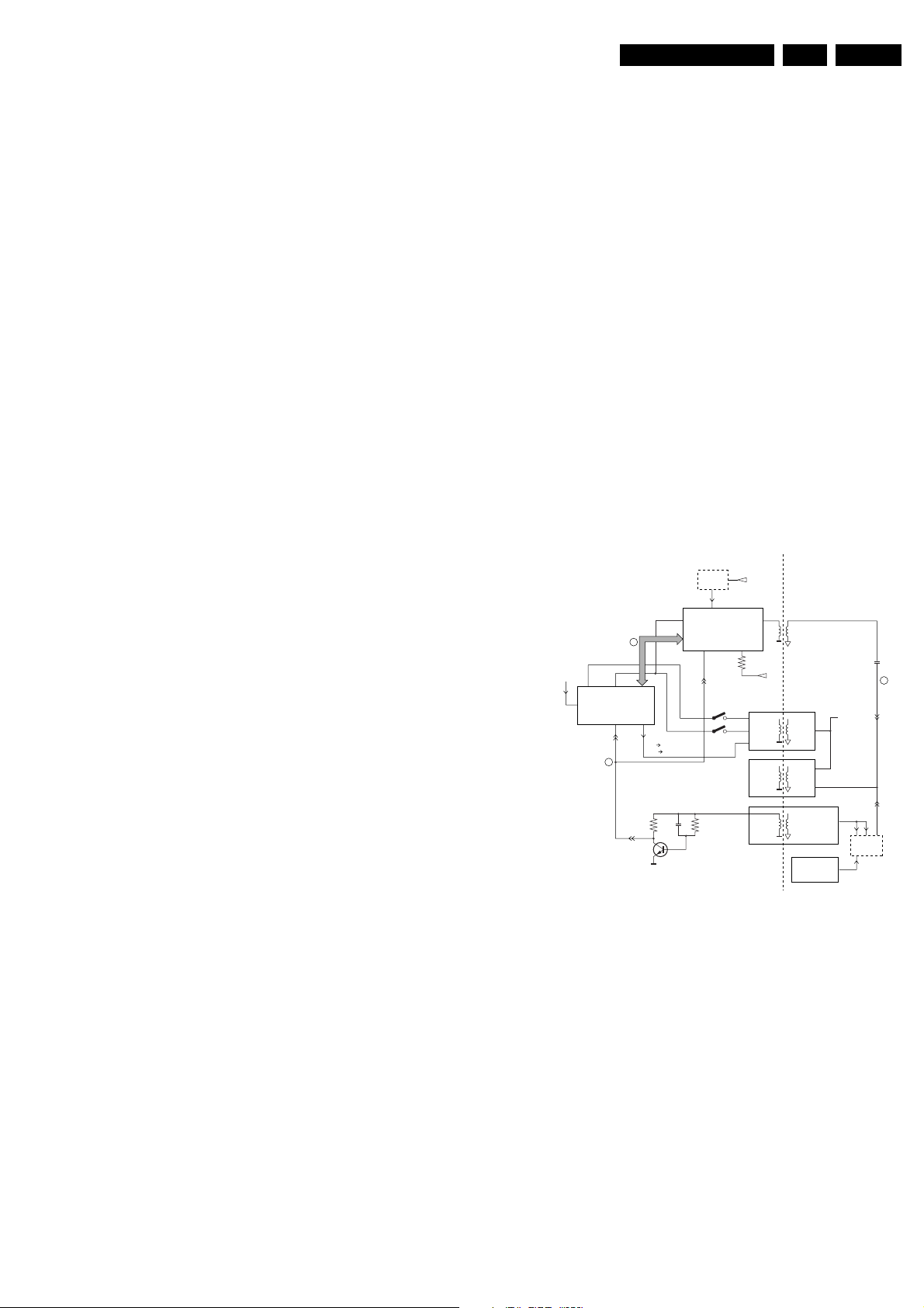
The "Protection Diagram" shows the structure of the protection
system. See diagram below.
7301
EHT-info
Flash detect
HFB
I2C
7001
I2C PROTECTIONS
HIP
HOP
PICNIC
TUNER
NVM
DNR
MSP
TOPIC
FBX
PROTECTION
PICNIC 3V3
+8V_CON
+5V_CON
I2C
CL 16532044_024.eps
Figure 5-3 Protection diagram
There are several types of protections:
• I2C related protections.
• OTC related protections (via polling on I/O pins or via
algorithms).
• HOP related protections (mainly for deflection items).
• Hardware errors that are not sensed by the OTC (e.g.
vertical flyback protection, bridge coil protection, E/W
protection, arcing protection).
All protections are explained below.
5.7.2 I2C Related Protections
In normal operation, some registers of the I2C controlled ICs
are refreshed every 200 ms. During this sequence, the I2C
busses and the I2C ICs are checked.
An I2C protection will take place if the SDA and SCL lines are
short-circuited to ground, or to each other. An I2C error will also
occur, if the power supply of the IC is missing (e.g. FBX_PROT
(error 16)).
5.7.3 OTC Related Protections
If a protection is detected at an OTC input, the OTC will start to
scan all protection inputs every 200 ms for 5 times. If the
protection on one of the inputs is still active after 1 s, the
microprocessor will put the set in the protection mode.
Before the scanning is started, a so-called "ESD refresh" is
carried out. This is done, because the interrupt on one of the
inputs is possibly caused either by a flash or by ESD. As a flash
or ESD can influence IC settings, the HIP, MSP, 3D Comb (US
only) and wireless module are initialised again, to ensure the
normal picture and sound conditions of the set.
8 V and 5 V protection: The microprocessor senses the
presence of the 8 V and 5 V (via the "+5V_CON" and
"+8V_CON" lines). If one (or both) of these voltages is (are) not
present, an error code is stored in the error buffer of the NVM,
and the set is put in the protection mode.
XPR (43)
HOP
FLS (5)
HFB-XRAY-PROT
+8V SENSE (105)
+5V SENSE (106)
OTC
I2C
090501
5.7.4 HOP Related Protections
Every 200 ms, the status register of the HOP is read by the
OTC (via the I2C bus). If a protection signal is detected on one
Service Modes, Error Codes, and Fault Finding
EN 29EM5.1E 5.
of the inputs of the HOP, the relevant error bit in the HOP
register is set to "high". If this error bit is still "high" after 1 s, the
OTC will store the error code in the error buffer of the NVM and,
depending on the relevancy of the error bit, the set will either
go into the protection mode or not.
The following protections are implemented:
• HFB (Horizontal Flyback): If the horizontal flyback is not
present, this is detected via the HOP (HFB_XRAY_PROT). One status bit is set to "high". The error code
is stored in the error buffer and the set will go into the
protection mode.
• XPR (X-ray protection): If the HFB pulses are too low
(level detection), the HOP will detect this via the XPR-bit.
The error will be logged in the error buffer and the set will
go into protection mode.
Note: Both errors will be logged as HFB-failure.
5.7.5 Hardware Related Protections
Due to the architecture ("hot" deflection), some protections
cannot be sensed by the microprocessor. Three of these
protections will lead to a protection on set level (Standby mode
and blinking LED), while another will only lead to a circuit
protection.
TV-set Protection
The following fault conditions will lead to a "complete" set
protection:
• BRIDGECOIL protection: This is sensed via the "EW"
signal going to the base of TS7652 (via R3495 and D6499).
In a normal situation, the voltage on C2498 (diagram A4) is
high and TS7652 is conducting. When bridge coil 5422
(diagram A3) is short circuited, the voltage on C2498
changes to low, which will block TS7652. In this case, also
TS7641 will block and the voltage on 2642 will rise until
TS7443 is forced in conduction. The "SUP-ENABLE"
signal (in normal operating condition -20 V) is shorted now
to ground level, which will force the Main Power Supply to
Standby mode.
• ARC protection: If there are "open" connections (e.g. bad
solder joints) in the high-energy deflection circuitry, this can
lead to damaging effects (read: fire). For that reason, the E/
W current is sensed (via 3479//3480). If this current
becomes too high, the "thyristor" circuit (TS7653 and
TS7654) is triggered. TS7442 is switched "on" and TS7443
is forced into conduction. . The "SUP-ENABLE" signal is
shorted now to ground level, which will force the Main
Power Supply to Standby mode.
• NON_VFB (No vertical Flyback) protection: If the frame
stage generates no pulses, TS7641 will block. TS7443 is
now switched "on", which will lead to Standby mode.
Therefore, in normal operation condition, TS7641 and
TS7652 are conducting, while TS7443 is blocked.
Circuit Protection
The following fault condition will lead to a "partly" set protection:
• PROT1 (DC) protection: When a DC-voltage (positive or
negative) is sensed on one of the loudspeaker outputs, the
protection circuit (TS7704, 7705, 7706 and 7707 in
diagram A6) will put the IC7700 in Standby mode (via tristate input pin 6). For more details, see chapter "Circuit
Descriptions".
5.8 Repair tips
5.8.1 Miscellaneous
The relay you hear when you switch the set "on" (from Standby
or via the mains switch), is from the degaussing circuitry. It is
not used for switching the Power Supply (as done in the MGchassis).
Take care not to touch the "hot" heatsink while disconnecting
the SSB, despite the fact that the mains cord is out of the mains
socket. There can still be an annoying rest-voltage on the
heatsink for a short while. This, because the discharge
resistors 3502 and 3503 (on the LSP between hot and cold
part) are not stuffed for Europe. Instead, discharge resistors
3066 and 3057 on the Mains Switch panel are used, but
because they are located before the Mains switch, they only
discharge when this switch is "on".
Advice: when you remove the SSB, disconnect the Mains
cord, but keep the Mains Switch "on".
Do not try to measure on the SSB side, which is facing the 'hot'
heatsink. This is dangerous. Most service test points are
guided to the 'tuner' side and are indicated by the 'service'
printing.
Where the circuitry was too "crowded" for service printing, you
can find the correct location on the "test point overviews" in this
manual.
A very large part of the LSP is "hot", such as:
• The primary part of the Standby Supply.
• The whole Main supply (except for the secondary Audio
supply).
• And the complete deflection circuitry (so notice that the
deflection coil is hot!).
5.8.2 Start-up Sequence
COLD
HOT
EHT-INFO
5
START/STOP
8V
RESET
5V
CON
8V
CON
106 105
POR
3
OTC
99 104
I2C BUS
1
STANDBY
low 7131/41 closed
high 7131/41 open
POR
7445
17/39
29
HOP
START/STOP
7141
7131
+11D
OUT
CUTOFF
(from
CRT panel)
5V
STBY
8V
SUPPLY
MAIN
SUPPLY
LINE DEFL.
(BRIDGECOIL
-PROT)
(ARC-PROT)
(NON-VFB)
Figure 5-4 Start-up circuitry
The start up sequence differs from other sets (e.g. MG-sets or
EM2E-sets, but is same as in EM3E-set):
1. When the set is switched "on", the 5 and 8 V lines
("+5V_CON" and "+8V_CON") of the standby power
supply are activated.
2. After the OTC senses them, the P will address the HOP via
the I2C-bus, to start the drive [1].
3. Via the "SUP-ENABLE" signal, the Main Supply is switched
"on" and will deliver the V_BAT to the Line deflection stage
[2].
4. EHT generation is now started.
5. The OTC will un-blank the picture.
6. When you switch "off" the set, this is done in a controlled
way via the POR signal [3].
Note: Standby is not directly achieved via the Standby line of
the microprocessor, but indirectly via the HOP circuitry.
Vbat
FRAME
DEFL
SUP-ENABLE
220 VAC
PROT-
SENSING
CL16532044_023.eps
2
140501

EN 30 EM5.1E5.
Service Modes, Error Codes, and Fault Finding
5.8.3 ComPair
This chassis does not have an IR transmitting LED (as in MGsets). Therefore, a "Service" (ComPair) connector is
implemented at the rear side of the set, which is directly
accessible (as in A10-, EM2E-, EM3E and EM5E-sets). In
addition to this, there is also a blinking LED procedure to show
the contents of the error buffer.
When you use ComPair, you have the possibility to activate a
"stepwise start-up" mode. With this mode, you can initiate the
start-up sequence step by step. This also means that in certain
steps, some protections are not activated. This is sometimes
very convenient during repair.
5.8.4 Protections
Activating SDM via the "service pads" will overrule the
processor-controlled protections, but not the hardware
protections. This means, that the A/D-input protections (5 and
8 V) and the I2C "not-acknowledging" info of the feature box
(FBX) and of the Tuner are overruled.
Caution: When doing this, the service technician must know
what he is doing, as it could lead to damaging the set.
The "ARC"- and/or "BRIDGECOIL" protection are hardly ever
triggered, however:
• When you suspect the "ARC" protection, look for bad
solder joints and smell. By interrupting resistor 3497, this
protection is disabled (special attention needed!).
• When you suspect the "BRIDGECOIL" protection, which
can also be due to a too wide picture amplitude, shorten G
and S of the E/W MOSFET 7480. This will disable the
protection. You will now have minimal horizontal amplitude.
Re-align the horizontal amplitude in the SAM menu and
remove the G/S short of TS7480.
5.8.7 Line Deflection
The simplest way is to replace the components of the Line
Deflection circuitry with repair kit 3122 785 90330.
5.8.8 Frame Deflection
Caution: When the Frame Deflection circuitry is suspected,
one must be careful. Because there is a DC-voltage on the
frame deflection, the beam current could damage the CRT
neck, leading to a defective CRT.
To prevent this from happening, you must:
1. Interrupt the resistors 3403 and 3404 on the CRT panel
(diagram F1), in order to remove the "filament" voltage
from the tube (no beam current, so no chance of destroying
the CRT).
2. Interrupt resistor 3403 on the LSP (diagram A4) to disable
the "SUP-ENABLE" line.
3. Measure with a multi-meter, or better with a oscilloscope,
the functionality of the Frame stage.
4. After you have found the cause, exchange the defective
component (e.g. TDA8177), and re-solder the interrupted
resistors.
5.8.5 Main Supply
The simplest way is, to replace the components of the Main
Supply with repair kit 3122 785 90310.
More detailed way:
1. Replace FET 7504 and zener 6505.
2. Remove the SSB panel.
3. Short B and E of TS7529, in order to put the Main Supply
in "on"-mode (TS7529 is blocking then).
Caution: To prevent that R3403 and TS7443 will be
damaged, first disable the HW-protection of the
deflection circuit. Therefore short circuit C2642 on the
LSP (diagram A4).
4. Attach a load of 500 O to V_BAT capacitor C2515 (the
supply can not work without a minimum load).
5. Use a variac, and slowly increase the V_MAINS. Measure
over sensing resistors R3514//15, if a nice sawtooth
voltage becomes available.
6. Also measure the V_BAT. This may never exceed +141 V.
If it does, there is something wrong in the feedback circuitry
(e.g. regulator 7506).
Note: Be careful when measuring on the gate of FET TS7504.
This circuitry is very high ohmic and can easily be damaged
(first connect ground to measuring equipment, than measure
the gate).
5.8.6 Standby Supply
The simplest way is to replace the components of the Standby
Supply with repair kit 3122 785 90460.
Loading...