


Página Web 1 de 57
Circuit Descriptions and Abbreviation List
Index of this chapter
1.Introduction
2.Block diagram
3.Power supply
4.Control
5.Tuner and IF
6.Video: HD jack interface
7.Video: High-end Input Processor
8.Video: Feature box
9.Video: High-end Output Processor
10.Video: 3D Comb Filter
11.Video: PIP/DW Panel
12.Synchronization
13.Horizontal deflection
14.Vertical deflection
15.Audio
16.CRT Panel / Rotation / Scavem
17.Software related features
18.Abbreviation list
19.IC Data Sheets
For a good understanding of the following circuit descriptions, please use the Block Diagram LSP Supply and Deflection, Block Diagram Video + DVI and DW, Block Diagram Video without DVI and DW, Block Diagram Audio, I2C Overview, Supply Lines Overview and Testpoints Overview (LSP (Copper Track Side), CRT Panel (FOR SETS WITH DW + DVI), CRT Panel (FOR SETS WITHOUT DW + DVI), DW Panel, SSB) and Wiring Diagram. Where necessary, you will find a separate drawing for clarification.
Introduction
The EM1.2U is a low end R8 chassis, with the same LSP, but with a Painter microprocessor (instead of the OTC).
The user interface and micro controller are the same as used in H8 sets. In the EM1.2U however, a HIP, PICNIC, and HOP are used for the '100 Hz' function instead of the BOCMA in the H8.
The HIP and HOP have about the same functionality as the BOCMA. This chip set insures that line frequency and YUV-signals are doubled (2 fH), while the vertical frequency stay 60 Hz (1fH). The set runs in progressive scan (an interlaced picture at 60 Hz, instead of at 30 Hz in normal NTSC).
The EM1.2U architecture consists of a full sized LSP/SSP combination, a smaller sized
11-02-2005
Página Web 2 de 57
SSB (mounted on the SSP via a SIMM connector), a PIP/DW panel, and a 3D Comb Filter panel.
The main functionalities of these boards are:
zLSP: supply, deflection, and sound amplification.
zSSP: tuner input, SIMM interface, I/O and interface provisions for extended functions such as PIP.
zSSB: core TV functionalities, such as set control, video and audio decoding, feature box, video featuring, and sync/geometry control.
The LSP (single sided) is designed very conventionally, with hardly any surface mounted components on the copper side.
Warning: be aware that the LSP has a very large 'hot' area, including both deflection coils.
The SSB is a high tech module (four layer, 2 sides reflow technology, full SMC) with very high component density and complete shielding for EMC reasons. Despite this, it is designed so that repair on component level still is possible. To achieve this, attention was paid to:
zThe position of service test lands: most of them are at the Tuner side.
zAccessibility (Tuner side). If there are still problems with the accessibility, one can order an extension board (12 NC: 9965 000 05769).
zClearance around surface mounted ICs (for replacing).
zDetailed diagnostics and fault finding is possible via ComPair.
Caution: Always be sure that the set is 'off' (disconnected from the AC Power) when you remove or replace the SSB panel!
Block Diagram
11-02-2005

Página Web 3 de 57
Figure: Block diagram
The Tuner/splitter (item 1200) is a PLL tuner and delivers the IF-signal, via audio and video SAW-filters, to the HIP (High-end Input Processor). The HIP has the following functions:
z IF modulation.
11-02-2005
Página Web 4 de 57
zVideo source select and record select.
zColor decoder.
zSynchronization.
Several video input/output connections (with audio connections) are available:
1.Side I/O: interfaces CVBS, SVSH.
2.AV1: interfaces CVBS, RGB-input and YUV-input (1fH)
3.AV2: interfaces CVBS and Y/C (meant for VCR-connection).
4.AV4: interfaces YPbPr/RGB (HD) inputs (2fH).
5.Monitor out: interfaces CVBS out.
6.Audio out: interfaces external front and surround speakers.
The HIP delivers YUV and sync signals to the PICNIC. This IC takes care of:
zAnalog to Digital conversion and vice versa.
zInterlaced to progressive scan conversion.
zPanorama mode.
zNoise reduction.
zDynamic contrast.
For Digital Scan, the PROZONIC is required, which can be connected to the PICNIC.
After the PICNIC, the YUV signals and sync signals are fed to the HOP (High-end Output Processor). This IC handles the video control and geometry part. The RGB-signals for CC/OSD (from the uP) are also inserted via the HOP. The video part delivers the RGB signals to the CRT-panel and the geometry part delivers the H-drive, V-drive, E/W-drive, and TILT-drive signals.
Both deflection circuits are 'hot' and located on the LSP. The HOP drives them. To make a galvanic separation, the Line Drive is driven via transformer 5410 and the Frame Drive via transformer 5621.The horizontal output stage generates some supply voltages and the EHT voltage, focus voltage and Vg2 voltage.
The RGB amplifiers on the CRT-panel are integrated in one IC, and are supplied with 200 V from the LOT.
The Scavem circuit modulates transitions of the Luminance (Y) signal on the horizontal deflection current, giving a sharper picture.
The sound part is built around the MSP34xx (Multi-channel Sound Processor) for IF sound detection, sound control and source selection. Dolby decoding is also done by the MSP. Amplification is done via a 'class B' integrated power amplifier IC, the TDA7497.
11-02-2005
Página Web 5 de 57
The microprocessor ('Painter') takes care of the analog CC input processing and output processing. The μP, ROM, and RAM are supplied with 3.3 V, which is derived from the +5V2.
The NVM (Non Volatile Memory) is used to store the settings, the Painter is an OTP (One Time Programmable) chip with integrated set software.
There is a separate Standby Supply, in order to reduce the Standby power consumption. During Standby, the Main Supply is switched 'off' (via TS7529). A relay (1550) is used to switch the Degaussing circuit. It is switched 'on' after set start-up and switched 'off' by the μP after 12 s.
The Main Supply, a SMPS based on the 'boost converter' principle, generates the 141 V (VBAT) and the +28V for the audio part.
Note: Voltage VBAT is not mains isolated ('hot'), but is alignment free.
Power Supply (Diagram A1 and A2)
The power supply has a number of main functions:
1.Mains harmonic filter.
2.Degaussing picture tube.
3.Standby power supply.
4.Main supply.
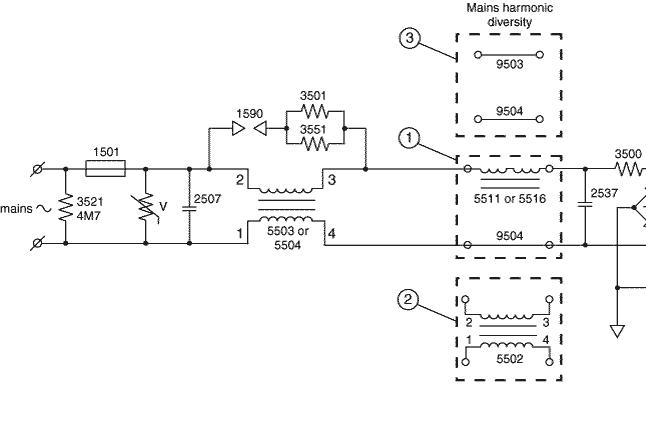
Mains Harmonic Filter (Diagram A1A)
11-02-2005
Página Web 6 de 57
Figure: Mains harmonic filter
The mains harmonic filter has two functions: to prevent high frequency signals (harmonics) from being transferred into the mains and to protect the set from lightning damage. Capacitor C2507 prevents the high frequency signals (generated by the set), from being conveyed into the mains (it forms a short-circuit).
In case of a lightning surge between the 2 phases (differential mode), the energy is immediately bled away through the VDR (R3509) to the other phase.
In case of a lightning surge on both phases of the mains in relation to the aerial ground (common mode), the filter acts as a high resistance (U EMK = L * dI/dt), as a result of which
the voltage across coil L5503/04 increases. A spark gap (1590) prevents the voltage from increasing too much, which would lead to a damaged coil. When ignited, the current will be discharged via this spark gap.
Resistor R3500 is used for limiting the inrush-current.
Degaussing (Diagram A1A)
As soon as the set is connected with the AC Power, the 5V2 is present. When the 'DEGAUSSING' signal from the processor (Painter) is 'low,' transistor 7528 will conduct, and relay 1550 is activated. Initially a considerable current will flow, via PTC 3516, through the degaussing coil. The PTC will heat up, resistance will rise, and the current will decay rapidly. The Painter makes the 'DEGAUSSING' signal 'high' after 12 seconds, which will switch 'off' the relay.
11-02-2005

Página Web 7 de 57
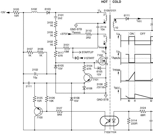
Standby power supply (Diagram A2)
Principle
This power supply is not only delivering the standby voltage, but also the main voltages for the small signal part. It is a SOPS type (Self-Oscillating Power Supply) and is regulated by the controlled switching of an oscillator. It uses the 'Flyback' principle:
Figure: Flyback principle
After closing switch 'S,' the current ID will increase linearly in time. The magnetic energy in the primary coil is directly proportional with the self-inductance of the coil and current ID (thus with the time the switch is closed).
The voltage polarity at the secondary winding is negative (due to different winding direction), meaning that diode D will block. Capacitor C will discharge via R L , and U OUT
will decrease.
Opening switch 'S' will generate a counter-e.m.f. in the primary winding, trying to maintain current I D . Through this the polarity of the secondary voltage will inverse. The magnetic
energy stored in the coil will now be transformed to the secondary side. Diode D will now conduct, capacitor C will be charged, and U OUT will increase.
Implementation
11-02-2005
Página Web 8 de 57
Figure: Standby supply circuitry
To apply this on the EM1.2U (diagram A2): replace switch 'S' by FET TS7102, coil L by L5100, diode D by D6111, and C by C2104.
zTime interval t0-t1: After switching 'on' the TV-set, the gate of MOSFET TS7102 will be high (max. 15 V due to zener diode D6105). This will drive the FET into saturation (UDS = 0 V). The DC-voltage UMAINS will be transposed across the primary winding of L5100 (3, 5), resulting in a linear increasing current through this coil. The voltage across the co-coupled coil (1, 2) is also positive and will keep the FET in conductivity via C2101, R3103/3105/3102 and R3117 for some time. The self-induction of the coil and the magnitude of the supply voltage (+375 V) determine the slope of the primary current. The maximum current is determined by the time the FET stays in conductance (t0-t1). This time is directly determined by the voltage across R3108//R3118 (0.7 Ω). This voltage is a measure of the current, and if it exceeds 1.4 V, TS7101 will be driven into conductivity and consequently connects the gate of
11-02-2005
Página Web 9 de 57
TS7102 to earth. The FET will block. The current is: 1.4 V / 0.7 Ω = 2 A. The voltage across the secondary winding (8, 9) will be negative, diodes D6111 and D6107 will block.
zTime interval t1-t2: The sudden current interruption in the primary coil will induce a counter-e.m.f. that tries to maintain the current. The voltage on the drain of the FET will increase. The secondary voltage (8, 10) will become positive and will charge C2104 via D6111. All energy that was stored in L5100 during t0-t1 will be transferred into the load. Due to the transformer principle, a voltage will now be induced in the primary winding (3, 5) and the co-coupled winding (1, 2). This voltage will be N* U SEC (N= winding ratio). The voltage across the co-coupled coil will be negative, keeping the FET blocked.
zTime t2: At t2, the current through the secondary coil will be reduced to zero, as C2104 is no longer charged. Consequently, the voltages will decay and will change polarity. The gate of the FET will be again made positive, is driven into conductivity, and the cycle starts again.
5V2 Stabilization and Feedback
The Standby Power Supply always oscillates at maximum power. The only limiting factor is the maximum primary current, which has been preset with R3108//3118.
R3113, zener diode D6122, R3124, and R3114 determine U OUT . If the voltage across
R3114 exceeds the threshold voltage of the diode of the optocoupler 7104 (± 1 V) or, in other words, UOUT exceeds 5.2 V, the transistor of the optocoupler will conduct. Transistor TS7100 is now driven, and a negative voltage will be transposed to the emitter of TS7101. When TS7101 conducts, the gate of the FET is at earth potential, forcing the oscillator to stop. Due to the load, the secondary voltage U OUT will decrease. At a certain
voltage, optocoupler TS7104 will block and the oscillator will start again.
Since there are no capacitors, and there is a high amplification factor in the feedback circuit, the feedback is ultra-fast. This is why the ripple on U OUT is minimal. The negative
supply voltage (-20 V) used in the feedback circuit originates from the co-coupling coil, and is rectified through D6103.
Stabilization is not effected through duty-cycle control, but through the burst-mode of TS7100.
Burst-mode is load dependent. If the power supply is less loaded, the secondary voltage will have the tendency to increase more rapidly. If the load on the power supply increases, then the oscillator stops less often, right up to the moment that the oscillator is operating continuously: maximum load. If the power supply is now loaded even more, the output voltage will decay. The maximum primary current set by R3108//3118 determines the maximum load.
8V6 Stabilization and Feedback
In general, with a flyback supply with multiple outputs, as used in the former chassis, one of
11-02-2005
Página Web 10 de 57
the output voltages is controlled via the primary feedback loop. The additional secondary output voltages are determined via the turn-ratio of the transformer.
It is often seen that a linear voltage regulator is used for post regulation of the non-primary regulated secondary voltages. The disadvantage of this approach is the power loss in the linear voltage regulator.
For this chassis, a power economic solution is achieved, by implementing a kind of secondary down-converter. The advantage, compared to a conventional down-converter, is that no extra coil is required. It is using the inductance of the main transformer. This way one large current coil, a power diode, and one elcap are saved.
11-02-2005
Página Web 11 de 57
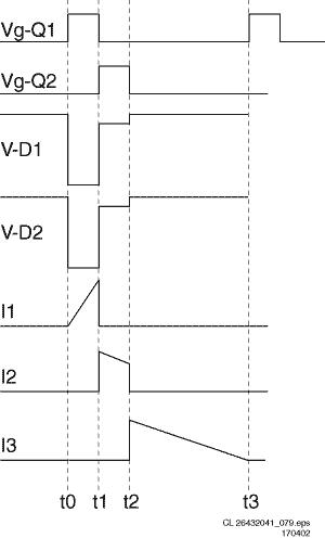
Figure: Circuit principle
A basic flyback converter is used, with a MOSFET Q1, transformer L1, and a primary feedback circuit. The output of the primary controlled voltage is U1.
The additional secondary controlled supply consists of D2 and Q2, with output voltage U2. The main flyback supply is working independently, where the duty cycle is controlled via the primary feedback, and the MOSFET Q1 is switching at a certain frequency. MOSFET Q2 is also switching at the same frequency, as it is synchronized with Q1.
11-02-2005
Página Web 12 de 57
Figure: Timing diagram
zTime interval t0-t1: The primary MOSFET Q1 is switched 'on,' both diodes D1 and D2 are blocked.
zTime interval t1-t2: MOSFET Q1 is switched 'off' and Q2 is switched 'on.' During this period, the energy is transferred to output U2 of the supply. Diode D1 is blocked, because U3 is lower than U1.
zTime t2: Q2 is switched 'off.'
zTime interval t2-t3: During this period, the rest of the energy will be transferred to output U1.
The two controllers, the primary feedback for U1, and the secondary feedback for U2, all work independently.
The secondary voltage U2 is controlled by the 'on' time of Q2.
As soon as the load on U2 increases, the 'on' time of Q2 (the period t1-t2) is automatically increased by the secondary feedback. More energy will be taken by the output U2, and less energy will be transferred to U1. Voltage U1 will drop automatically. The primary feedback
11-02-2005
Página Web 13 de 57
loop will change the primary drive to enlarge the total amount of energy to be transferred, from the primary side, and U1 will rise again.
Protection
If the optocoupler fails, the secondary voltage will increase. This would have disastrous consequences since many ICs (for example, Painter, Flash-RAM and DRAM) are fed with this 5.2 V. In other words, very expensive repairs would be required.
We already know that the negative supply is directly dependent upon the secondary 5.2 V, because of which the negative supply will increase proportionally as the secondary voltage increases.
If the negative supply, in the mean time, reaches -25 V, D6106 will start to zener and TS7101 will start conducting. D6106 will take over the stabilization task of the optocoupler, however, with a considerable spread: from -20 to -25 V is a 25 % increase, thus UOUT will increase from 5.2 V to a maximum of 6.5 V.
Tuner Supply
The Standby supply produces the +33V (V TUN ) voltage for the tuner. The +33V is the
tuning voltage for the Tuner. The +5VT voltage is derived from the +8V with stabilizer 7912 (see diagram A8). It is used to supply the tuner only.
SSB Supply
There are several voltages going to the SSB: +8V6, +5V2 and +3V3.
The +5V2 and +8V6 (always present) come directly from the Standby power supply. The +3V3 is derived from the +5V with stabilizer 7910 (diagram A8).
Main Supply (Diagram A1)
The main power supply is able to deliver continuous power between 100 W and 160 W. Some important notes:
zV BAT is not isolated from the main supply ('hot').
zV BAT is alignment free.
Principle
The Main Power Supply generates the 141 V (V BAT ) and the +28V for the audio part. It is based on the 'buck booster' principle. A booster converter produces an output voltage, which is greater than its input voltage. This is necessary in order to get a stable V BAT out of
the 110 V AC power input voltage.
11-02-2005

Página Web 14 de 57
Figure: 'Buck boost' principle
1.After closing switch 'S', a linear in time increasing current IT will flow through inductor L.
2.Opening switch 'S' will generate a counter-e.m.f. in coil L, trying to maintain the current. This is possible via diode D (this diode is also called the 'freewheel diode'). Therefore, after opening 'S', the magnetic energy stored in coil L will be transferred to
11-02-2005
Página Web 15 de 57
electrostatic energy in capacitor C.
3. So, by changing the duty cycle, it will be possible to control V BAT .
Implementation
At start-up of the main supply, C2515 (diagram A1B) can be assumed to be a short-circuit. UAB will be 15 V (R3513, D6510) and UGS of the FET will be +5.4 V (via D6515). The FET will be driven into saturation (same as closing switch 'S'). The drain-current will increase linearly in time. With other words: resistors R3513 and R3518 will start the oscillator. The voltage across the co-coupled coil (5, 6) will keep the FET in conductivity.
The TS7502 is a low-voltage semiconductor, which drives the MOSFET TS7504. To bridge the different voltage levels, an opto-coupler (item 7507) is used. Via this opto-coupler, the DC-current through R3504 is influenced. The changed current through R3504 changes the VBE of TS7502, which will influence the drive of MOSFET TS7504 (= switch 'S' in figure 'Buck boost principle').
The sudden current interruption in the primary coil will induce a counter-e.m.f. that tries to maintain the current via the 'freewheel' diode D6534. This current is linearly decreasing in time and, as it is also flowing through R3514//R3515, TS7502 will be blocked after a certain period. The gate of the FET will be made positive again, is driven into conductivity, and the cycle starts again.
For safety reasons, transistor TS7530 is added as a back-up solution for TS7502. If B-E of TS7502 is shorted, TS7530 takes over its function.
Stabilization of V BAT
The output voltage VBAT is determined by: V BAT = V IN * (T ON / (T ON + T OFF )) = V IN * duty-cycle.
To stabilize the output voltage, a feedback loop is implemented, which will reduce T ON when V BAT increases and vice versa.
Via a voltage divider, existing of (1 %) resistors R3507, R3510, and R3527//3549, a voltage of 2.5 V (when VBAT = 141 V) is fed to the input of precision shunt regulator 7506. This regulator will conduct, and a current will flow through the diode part of the opto-coupler 7507. The base of TS7502 will now be set at a certain positive voltage. As this transistor switches the FET TS7504 'on' and 'off,' this circuit can determine the duty-cycle.
For example, when the load increases, V BAT will decrease. Consequently, the input
voltage of regulator 7506 will decrease, resulting in a lower current. Via opto-coupler 7505 and transistor TS7502, T ON of the FET is changed (will increase). The output voltage V
BAT will rise.
If the load continues to increase, the regulator will block at a certain moment. TON is now
11-02-2005
Página Web 16 de 57
at maximum value. This is the point where V BAT will go below 141 V and, at further
increasing load, is switched 'off.' The voltage across the co-coupled coil (L5506, pin 4 and 5) will decrease, due to the increasing load. Therefore, the voltage on the gate of TS7504 comes below the threshold voltage. The supply switches 'off,' and an audible hiccupping can be heard.
On the other hand, when the load decreases, V BAT will rise. Consequently, the input
voltage of TS7506 will also rise, resulting in a higher current. This changes the base voltage of TS7502, and through that the T ON of the FET will decrease. The output voltage
V BAT will be reduced.
If, for instance, V IN decreases (for example, U MAINS is 90 V instead of 120 V), the slope of the drain-current will be flattened, through which the FET will be in conductance longer, keeping V OUT constant.
If, for any reason, the stabilization circuit fails, the output voltage V BAT can never exceed 200 V (via D6514). D6514 will form a short-circuit, V BAT will drop and the set will switch 'off' (this will also result in an audible hiccupping of the supply).
Switch to 'Standby' (via RC)
When the set is switched to 'Standby' mode via the Remote Control, the Main supply is switched 'off' by the circuit around TS7529 (see diagram A1).
During 'on'-state, the Main supply is fed with line pulses via the 'SUP-ENABLE' line. They are rectified and smoothed via D6517, D6516, and C2530, and fed to TS7529. Because they are less than -20 V, this transistor is blocked. When these pulses are stopped, TS7529 will be saturated and TS7502 will switch 'on.' This will switch 'off' the Main supply.
It is important, that the Main supply is switched 'off' before the Standby supply. This is in order to prevent several unwanted phenomena, such as audible plops and visible switch off spots. Without an extra circuit to force this, this cannot be achieved. Therefore, the circuit around TS7505 and TS7508 (diagram A1A) is implemented.
This circuit compares the Main DC voltage (+375 V) and a reference voltage (V BAT ) via
resistors R3554, R3555, R3560, and R3556. Elcap C2539 serves as voltage source for the two transistors.
When the Main DC voltage will decrease w.r.t. the reference voltage VBAT, the 'SUP_ENABLE' line will be activated via TS7505, TS7508 and R3559. This will switch 'off' the Main supply via TS7529.
Switch to 'On' (via 'SUP-ENABLE')
Via the 'STANDBY' command from the Painter, the MOSFETS 7141 and 7131 (diagram A2) are switched 'on.' When the Painter senses the +5V and +8V, a command is given to
the HOP to start the drive (via I 2 C).
When this is sensed via the 'SUP-ENABLE' line (at the base of line transistor TS7421, diagram A3), the main supply is switched 'on' via TS7529 (diagram A1).
11-02-2005
Página Web 17 de 57
Protection
When, for any reason (interruptions or defective components), the feedback loop of the Main supply fails, the V BAT will rise. This is detected via zener diodes D6507, D6508, and
D6513. This will 'ignite' thyristor T7503, which will result in the blowing of fuse 1503.
Audio Supply
The pulses on the secondary winding of L5506 (or L5512) are rectified by D6535 (+16 V) and D6536 (-16V), and smoothed by C2542 and C2543.
Control (Diagram B7)
Painter
Introduction
The SAA5667 (IC7001) is called the Painter. The microprocessor and the CC/OSD-decoder are integrated in this IC. Some of its functions are:
zSet control.
zCC/OSD acquisition.
zRGB-outputs to the HOP
zMenu blending; for blending the contrast, software controlled.
zI/O-ports for I 2 C, RC5, LED, and service modes.
zError code generation.
Data Storage
zThe set software is integrated in the Painter.
zThe Non Volatile Memory IC7001 is a 4 kB version M24C32, and is used to store data of a working set.
Power Supply
The Painter is supplied with 3V3. For this voltage, a 3V3 stabilizer is used (IC7005). With the circuitry around TS7003 and 7004 (diagram B7), a reset is generated to wake up the Painter (pin 74). During this reset, all I/O pins of the Painter are made 'high.'
CC/OSD
11-02-2005
Página Web 18 de 57
The horizontal (H D ) and vertical (V SYNC ) sync pulses are also fed to the Painter for stable OSD and CC.
This IC gets its video signal directly (from the HIP) on pin 31. The RGB-outputs (46/47/48) together with the fast blanking signal (pin 52) are fed to the HOP.
I 2 C Bus
There are two I 2 C busses used:
zSlow (max. 100 kHz) hardware I 2 C-bus (called SDA_S/SCL_S), used for all ICs.
zSeparate short bus (called SDA_NVM/SCL_NVM) for the Non Volatile Memory (NVM), to avoid data corruption.
Note: In the diagrams you can also find a bus called SDA_F/SCL_F (F= fast), but in this chassis it is connected to the 'slow' bus.
NVM
The Non Volatile Memory contains all set related data that must be kept permanently, such as:
zSoftware identification.
zOperational hours.
zError codes.
zOption codes.
zAll factory alignments.
zLast Status items for the customer + a complete factory recall.
Tuner and IF (Diagram A8 and B2)
The tuner/splitter is I 2 C controlled, and is capable of receiving off-air and cable channels.
Tuning is done via I 2 C. The reference voltage on pin 9 is 33 V. This voltage (V TUN ) is derived from the secondary side of the standby supply, via D6110 and R3116//R3115 and a 33 V zener diode (D6200). The Painter, together with the HIP, controls the tuning procedure. There is also automatic switching for the different video systems.
The IF-filter is integrated in a SAW (Surface Acoustic Wave) filter. The type of this filter depends on the received standard(s). There are two SAW filters: one for filtering picture-IF and a second one for sound-IF.
The output of the tuner is controlled via an IF-amplifier with AGC-control. This is a voltage
11-02-2005
 Loading...