


EMERSON LF501EM4
Table of contents
 Loading...
50” LCD TV
chassis FL13.16
© 2013 Funai Electric Co., Ltd.
All rights reserved. No part of this manual may be reproduced, copied, transmitted, disseminated, transcribed,
downloaded or stored in any storage medium, in any form or for any purpose without the express prior written
consent of Funai. Furthermore, any unauthorized commercial distribution of this manual or any revision hereto
is strictly prohibited.
Information in this document is subject to change without notice. Funai reserves the right to change the content
herein without the obligation to notify any person or organization of such changes.
with the design is a registered trademark of Funai Electric Co., Ltd and may not be used in any way
without the express written consent of Funai. All other trademarks used herein remain the exclusive property of
their respective owners. Nothing contained in this manual should be construed as granting, by implication or
otherwise, any license or right to use any of the trademarks displayed herein. Misuse of any trademarks or any
other content in this manual is strictly prohibited. Funai shall aggressively enforce its intellectual property rights
to the fullest extent of the law.
SERVICE MANUAL
Contents
This service manual contains information of different types of models.
Make sure to refer to the section describing your model.
TYPE A
LF501EM4 EMERSON (Serial No.: DS1)
50ME313V/F7 MAGNAVOX (Serial No.: DS1)
TYPE B
50ME313V/F7 MAGNAVOX (Serial No.: DS2)
LF501EM4 EMERSON (Serial No.: DS2)
130327

IMPORTANT SAFETY NOTICE
Proper service and repair is important to the safe, reliable operation of all
Funai Equipment. The service procedures recommended by Funai and
described in this service manual are effective methods of performing
service operations. Some of these service special tools should be used
when and as recommended.
It is important to note that this service manual contains various CAUTIONS
and NOTICES which should be carefully read in order to minimize the risk
of personal injury to service personnel. The possibility exists that improper
service methods may damage the equipment. It also is important to
understand that these CAUTIONS and NOTICES ARE NOT EXHAUSTIVE.
Funai could not possibly know, evaluate and advice the service trade of all
conceivable ways in which service might be done or of the possible
hazardous consequences of each way. Consequently, Funai has not
undertaken any such broad evaluation. Accordingly, a servicer who uses a
service procedure or tool which is not recommended by Funai must first
use all precautions thoroughly so that neither his safety nor the safe
operation of the equipment will be jeopardized by the service method
selected.
The LCD panel is manufactured to provide many years of useful life.
Occasionally a few non active pixels may appear as a tiny spec of color.
This is not to be considered a defect in the LCD screen.

TABLE OF CONTENTS
Specifications . . . . . . . . . . . . . . . . . . . . . . . . . . . . . . . . . . . . . . . . . . . . . . . . . . . . . . . . . . . . . . . . . . . . . . . . . . . 1-1
Important Safety Precautions . . . . . . . . . . . . . . . . . . . . . . . . . . . . . . . . . . . . . . . . . . . . . . . . . . . . . . . . . . . . . . . 2-1
Standard Notes for Servicing . . . . . . . . . . . . . . . . . . . . . . . . . . . . . . . . . . . . . . . . . . . . . . . . . . . . . . . . . . . . . . . 3-1
Cabinet Disassembly Instructions . . . . . . . . . . . . . . . . . . . . . . . . . . . . . . . . . . . . . . . . . . . . . . . . . . . . . . . . . . . 4-1
Electrical Adjustment Instructions . . . . . . . . . . . . . . . . . . . . . . . . . . . . . . . . . . . . . . . . . . . . . . . . . . . . . . . . . . . . 5-1
How to Initialize the LCD TV . . . . . . . . . . . . . . . . . . . . . . . . . . . . . . . . . . . . . . . . . . . . . . . . . . . . . . . . . . . . . . . . 6-1
Firmware Renewal Mode . . . . . . . . . . . . . . . . . . . . . . . . . . . . . . . . . . . . . . . . . . . . . . . . . . . . . . . . . . . . . . . . . . 7-1
Troubleshooting. . . . . . . . . . . . . . . . . . . . . . . . . . . . . . . . . . . . . . . . . . . . . . . . . . . . . . . . . . . . . . . . . . . . . . . . . . 8-1
Block Diagrams [TYPE A] . . . . . . . . . . . . . . . . . . . . . . . . . . . . . . . . . . . . . . . . . . . . . . . . . . . . . . . . . . . . . . . . . . 9-1
[TYPE B] . . . . . . . . . . . . . . . . . . . . . . . . . . . . . . . . . . . . . . . . . . . . . . . . . . . . . . . . . . . . . . . . . . 9-6
Schematic Diagrams / CBA and Test Points . . . . . . . . . . . . . . . . . . . . . . . . . . . . . . . . . . . . . . . . . . . . . . . . . . . 10-1
Wiring Diagram [TYPE A] . . . . . . . . . . . . . . . . . . . . . . . . . . . . . . . . . . . . . . . . . . . . . . . . . . . . . . . . . . . . . . . . . 11-1
[TYPE B] . . . . . . . . . . . . . . . . . . . . . . . . . . . . . . . . . . . . . . . . . . . . . . . . . . . . . . . . . . . . . . . . . 11-2
Exploded Views . . . . . . . . . . . . . . . . . . . . . . . . . . . . . . . . . . . . . . . . . . . . . . . . . . . . . . . . . . . . . . . . . . . . . . . . 12-1
Parts List . . . . . . . . . . . . . . . . . . . . . . . . . . . . . . . . . . . . . . . . . . . . . . . . . . . . . . . . . . . . . . . . . . . . . . . . . . . . . 13-1
Revision History . . . . . . . . . . . . . . . . . . . . . . . . . . . . . . . . . . . . . . . . . . . . . . . . . . . . . . . . . . . . . . . . . . . . . . . . 14-1
1-1 FL13.16SP
SPECIFICATIONS
< TUNER / NTSC >
ANT. Input ---------------------- 75 Ω Unbal., F type
< TUNER / ATSC >
< LCD PANEL >
< VIDEO >
< AUDIO >
All items are measured across 8 Ω load at speaker output terminal with L.P.F.
Description Condition Unit Nominal Limit
1. AFT Pull-In Range --- MHz ±2.3 ±2.1
2. Synchronizing Sens.
TV.ch.4
CA.ch.31
CA.ch.87
dBµV
dBµV
dBµV
18
18
18
20
20
23
Description Condition Unit Nominal Limit
1. Received Freq. Range (-28dBm) --- kHz --- ±100
2. ATSC Dynamic Range (min / max)
ch.4
ch.10
ch.41
dBm
dBm
dBm
---
---
---
-76/0
-76/0
-76/+4
Description Condition Unit Nominal Limit
1. Native Pixel Resolution
Horizontal
Verti cal
pixels
pixels
1920
1080
---
---
2. Brightness (w / filter) ---
cd/m
2
270 ---
3. Viewing Angle
Horizontal
Verti cal
°
°
-88 to 88
-88 to 88
---
---
Description Condition Unit Nominal Limit
1. Over Scan
Horizontal
Verti cal
%
%
5
5
5±5
5±5
2. Color Temperature
---
x
y
°K 12000
0.272
0.278
---
±3%
±3%
<Measurement condition>
Input signal: HDMI1 Raster (40/80IRE) 1080i@60
Measurement point: Screen center
Measuring instrument:
Made of KONICA MINOLTA Luminance meter CA-310
Aging time: 60min. (Retail MODE / 100IRE Raster HDMI
1080i@60)
MODE setting of TV: Shipment setting / Retail MODE
Ambient temperature: 25°C ±5°C
3. Resolution (composite video)
Horizontal
Verti cal
line
line
400
350
---
---
Description Condition Unit Nominal Limit
1.
Audio MAX Output (ATSC 0dBfs)
Lch/Rch W 10.0/10.0 9.0/9.0
2. Audio Distortion (NTSC) 500mW: Lch/Rch % 0.5/0.5 2.0/2.0
2-1 LTVN_ISP
IMPORTANT SAFETY PRECAUTIONS
Prior to shipment from the factory, our products are strictly inspected for recognized product safety and electrical
codes of the countries in which they are to be sold. However, in order to maintain such compliance, it is equally
important to implement the following precautions when a set is being serviced.
Safety Precautions for LCD TV
Circuit
1. Before returning an instrument to the
customer, always make a safety check of the
entire instrument, including, but not limited to, the
following items:
a. Be sure that no built-in protective devices are
defective and have been defeated during
servicing. (1) Protective shields are provided
on this chassis to protect both the technician
and the customer. Correctly replace all missing
protective shields, including any removed for
servicing convenience. (2) When reinstalling
the chassis and/or other assembly in the
cabinet, be sure to put back in place all
protective devices, including but not limited to,
nonmetallic control knobs, insulating
fishpapers, adjustment and compartment
covers/shields, and isolation resistor/capacitor
networks. Do not operate this instrument or
permit it to be operated without all
protective devices correctly installed and
functioning. Servicers who defeat safety
features or fail to perform safety checks
may be liable for any resulting damage.
b. Be sure that there are no cabinet openings
through which an adult or child might be able to
insert their fingers and contact a hazardous
voltage. Such openings include, but are not
limited to, (1) spacing between the Liquid
Crystal Panel and the cabinet mask, (2)
excessively wide cabinet ventilation slots, and
(3) an improperly fitted and/or incorrectly
secured cabinet back cover.
c. Antenna Cold Check - With the instrument AC
plug removed from any AC source, connect an
electrical jumper across the two AC plug
prongs. Place the instrument AC switch in the
on position. Connect one lead of an ohmmeter
to the AC plug prongs tied together and touch
the other ohmmeter lead in turn to each tuner
antenna input exposed terminal screw and, if
applicable, to the coaxial connector. If the
measured resistance is less than 1.0 megohm
or greater than 5.2 megohm, an abnormality
exists that must be corrected before the
instrument is returned to the customer. Repeat
this test with the instrument AC switch in the off
position.
d. Leakage Current Hot Check - With the
instrument completely reassembled, plug the
AC line cord directly into a 120 V AC outlet. (Do
not use an isolation transformer during this
test.) Use a leakage current tester or a
metering system that complies with American
National Standards Institute (ANSI) C101.1
Leakage Current for Appliances and
Underwriters Laboratories (UL) 1410, (50.7).
With the instrument AC switch first in the on
position and then in the off position, measure
from a known earth ground (metal water pipe,
conduit, etc.) to all exposed metal parts of the
instrument (antennas, handle brackets, metal
cabinet, screw heads, metallic overlays, control
shafts, etc.), especially any exposed metal
parts that offer an electrical return path to the
chassis. Any current measured must not
exceed 0.5 milli-ampere. Reverse the
instrument power cord plug in the outlet and
repeat the test.
ANY MEASUREMENTS NOT WITHIN THE
LIMITS SPECIFIED HEREIN INDICATE A
POTENTIAL SHOCK HAZARD THAT MUST
BE ELIMINATED BEFORE RETURNING THE
INSTRUMENT TO THE CUSTOMER OR
BEFORE CONNECTING THE ANTENNA OR
ACCESSORIES.
2. Read and comply with all caution and safety-
related notes on or inside the receiver cabinet, on
the receiver chassis, or on the Liquid Crystal
Panel.
ALSO TEST WITH
PLUG REVERSED
USING AC
ADAPTER PLUG
AS REQUIRED
TEST ALL EXPOSED
METAL SURFACES
READING SHOULD
NOT BE ABOVE 0.5 mA
EARTH
GROUND
_
DEVICE
LEAKAGE
CURRENT
TESTER
+
BEING
TESTED

2-2 LTVN_ISP
3. Design Alteration Warning - Do not alter or add
to the mechanical or electrical design of this TV
receiver. Design alterations and additions,
including, but not limited to circuit modifications
and the addition of items such as auxiliary audio
and/or video output connections, might alter the
safety characteristics of this receiver and create a
hazard to the user. Any design alterations or
additions will void the manufacturer's warranty and
may make you, the servicer, responsible for
personal injury or property damage resulting
therefrom.
4. Hot Chassis Warning -
a. Some TV receiver chassis are electrically
connected directly to one conductor of the AC
power cord and maybe safety-serviced without
an isolation transformer only if the AC power
plug is inserted so that the chassis is
connected to the ground side of the AC power
source. To confirm that the AC power plug is
inserted correctly, with an AC voltmeter,
measure between the chassis and a known
earth ground. If a voltage reading in excess of
1.0 V is obtained, remove and reinsert the AC
power plug in the opposite polarity and again
measure the voltage potential between the
chassis and a known earth ground.
b. Some TV receiver chassis normally have 85V
AC(RMS) between chassis and earth ground
regardless of the AC plug polarity. This chassis
can be safety-serviced only with an isolation
transformer inserted in the power line between
the receiver and the AC power source, for both
personnel and test equipment protection.
c. Some TV receiver chassis have a secondary
ground system in addition to the main chassis
ground. This secondary ground system is not
isolated from the AC power line. The two
ground systems are electrically separated by
insulation material that must not be defeated or
altered.
5. Observe original lead dress. Take extra care to
assure correct lead dress in the following areas: a.
near sharp edges, b. near thermally hot parts-be
sure that leads and components do not touch
thermally hot parts, c. the AC supply, d. high
voltage, and, e. antenna wiring. Always inspect in
all areas for pinched, out of place, or frayed wiring.
Check AC power cord for damage.
6. Components, parts, and/or wiring that appear to
have overheated or are otherwise damaged
should be replaced with components, parts, or
wiring that meet original specifications.
Additionally, determine the cause of overheating
and/or damage and, if necessary, take corrective
action to remove any potential safety hazard.
7. Product Safety Notice - Some electrical and
mechanical parts have special safety-related
characteristics which are often not evident from
visual inspection, nor can the protection they give
necessarily be obtained by replacing them with
components rated for higher voltage, wattage, etc.
Parts that have special safety characteristics are
identified by a # on schematics and in parts lists.
Use of a substitute replacement that does not
have the same safety characteristics as the
recommended replacement part might create
shock, fire, and/or other hazards. The product's
safety is under review continuously and new
instructions are issued whenever appropriate.
Prior to shipment from the factory, our products
are strictly inspected to confirm they comply with
the recognized product safety and electrical codes
of the countries in which they are to be sold.
However, in order to maintain such compliance, it
is equally important to implement the following
precautions when a set is being serviced.

2-3 LTVN_ISP
Precautions during Servicing
A. Parts identified by the # symbol are critical for
safety.
Replace only with part number specified.
B. In addition to safety, other parts and assemblies
are specified for conformance with regulations
applying to spurious radiation. These must also be
replaced only with specified replacements.
Examples: RF converters, RF cables, noise
blocking capacitors, and noise blocking filters, etc.
C. Use specified internal wiring. Note especially:
1) Wires covered with PVC tubing
2) Double insulated wires
3) High voltage leads
D. Use specified insulating materials for hazardous
live parts. Note especially:
1) Insulation Tape
2) PVC tubing
3) Spacers
4) Insulators for transistors.
E. When replacing AC primary side components
(transformers, power cord, etc.), wrap ends of
wires securely about the terminals before
soldering.
F. Observe that the wires do not contact heat
producing parts (heat sinks, oxide metal film
resistors, fusible resistors, etc.)
G. Check that replaced wires do not contact sharp
edged or pointed parts.
H. When a power cord has been replaced, check that
11~13 lb (5~6 kg) of force in any direction will not
loosen it.
I. Also check areas surrounding repaired locations.
J. Use care that foreign objects (screws, solder
droplets, etc.) do not remain inside the set.
K. When connecting or disconnecting the internal
connectors, first, disconnect the AC plug from the
AC supply outlet.
L. When installing parts or assembling the cabinet
parts, be sure to use the proper screws and
tighten certainly.

2-4 LTVN_ISP
Safety Check after Servicing
Examine the area surrounding the repaired location for damage or deterioration. Observe that screws, parts and
wires have been returned to original positions. Afterwards, perform the following tests and confirm the specified
values in order to verify compliance with safety standards.
1. Clearance Distance
When replacing primary circuit components, confirm
specified clearance distance (d) and (d') between
soldered terminals, and between terminals and
surrounding metallic parts. (See Fig. 1)
Table 1: Ratings for selected area
Note: This table is unofficial and for reference only. Be
sure to confirm the precise values.
2. Leakage Current Test
Confirm the specified (or lower) leakage current
between B (earth ground, power cord plug prongs) and
externally exposed accessible parts (RF terminals,
antenna terminals, video and audio input and output
terminals, microphone jacks, earphone jacks, etc.) is
lower than or equal to the specified value in the table
below.
Measuring Method: (Power ON)
Insert load Z between B (earth ground, power cord plug
prongs) and exposed accessible parts. Use an AC
voltmeter to measure across both terminals of load Z.
See Fig. 2 and following table.
Table 2: Leakage current ratings for selected areas
Note: This table is unofficial and for reference only. Be sure to confirm the precise values.
AC Line Voltage Region
Clearance
Distance (d), (d’)
110 to 130 V
U.S.A. or
Canada
≥ 3.2 mm
(0.126 inches)
AC Line Voltage Region Load Z Leakage Current (i) Earth Ground (B) to:
110 to 130 V
U.S.A. or
Canada
0.15 µF CAP. & 1.5 kΩ
RES. Connected in parallel
i ≤ 0.5 mA rms
Exposed accessible
parts
Chassis or Secondary Conductor
Primary Circuit
Fig. 1
d' d
AC Voltmeter
(High Impedance)
Exposed Accessible Part
B
Earth Ground
Power Cord Plug Prongs
Z
Fig. 2
3-1 TVN_SN
STANDARD NOTES FOR SERVICING
Circuit Board Indications
1. The output pin of the 3 pin Regulator ICs is
indicated as shown.
2. For other ICs, pin 1 and every fifth pin are
indicated as shown.
3. The 1st pin of every male connector is indicated as
shown.
Pb (Lead) Free Solder
Pb free mark will be found on PCBs which use Pb
free solder. (Refer to figure.) For PCBs with Pb free
mark, be sure to use Pb free solder. For PCBs
without Pb free mark, use standard solder.
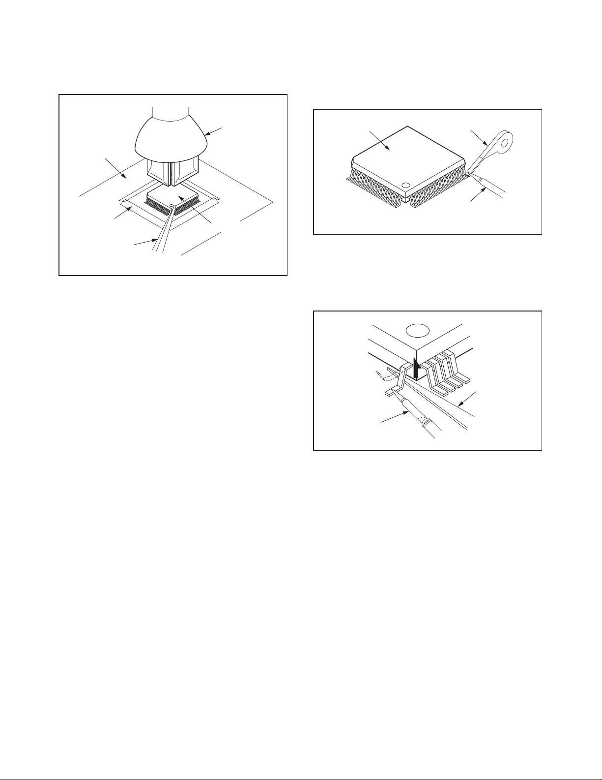
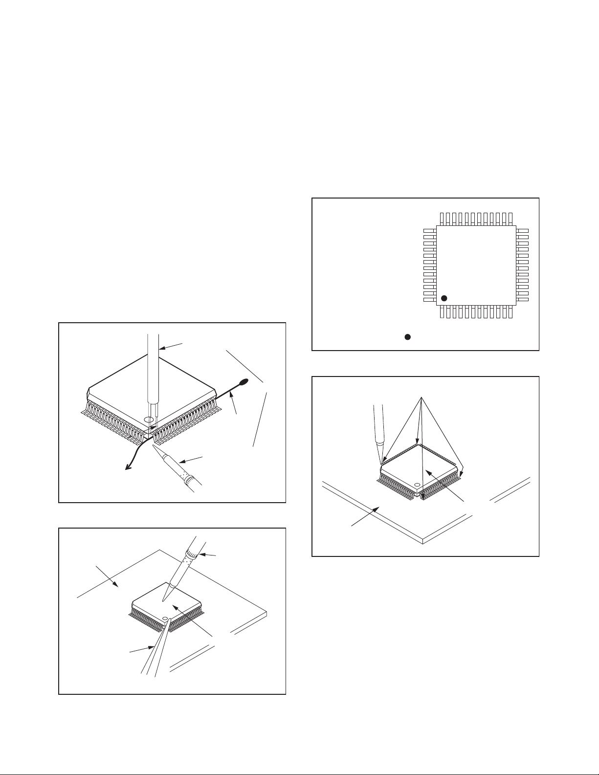
How to Remove / Install Flat Pack-IC
1. Removal
With Hot-Air Flat Pack-IC Desoldering Machine:
1. Prepare the hot-air flat pack-IC desoldering
machine, then apply hot air to the Flat Pack-IC
(about 5 to 6 seconds). (Fig. S-1-1)
2. Remove the flat pack-IC with tweezers while
applying the hot air.
3. Bottom of the flat pack-IC is fixed with glue to the
CBA; when removing entire flat pack-IC, first apply
soldering iron to center of the flat pack-IC and heat
up. Then remove (glue will be melted). (Fig. S-1-6)
4. Release the flat pack-IC from the CBA using
tweezers. (Fig. S-1-6)
CAUTION:
1. The Flat Pack-IC shape may differ by models. Use
an appropriate hot-air flat pack-IC desoldering
machine, whose shape matches that of the Flat
Pack-IC.
2. Do not supply hot air to the chip parts around the
flat pack-IC for over 6 seconds because damage
to the chip parts may occur. Put masking tape
around the flat pack-IC to protect other parts from
damage. (Fig. S-1-2)
Top View
Out
In
Bottom View
Input
5
10
Pin 1
Pin 1
Pb free mark
Fig. S-1-1
3-2 TVN_SN
3. The flat pack-IC on the CBA is affixed with glue, so
be careful not to break or damage the foil of each
pin or the solder lands under the IC when
removing it.
With Soldering Iron:
1. Using desoldering braid, remove the solder from
all pins of the flat pack-IC. When you use solder
flux which is applied to all pins of the flat pack-IC,
you can remove it easily. (Fig. S-1-3)
2. Lift each lead of the flat pack-IC upward one by
one, using a sharp pin or wire to which solder will
not adhere (iron wire). When heating the pins, use
a fine tip soldering iron or a hot air desoldering
machine. (Fig. S-1-4)
3. Bottom of the flat pack-IC is fixed with glue to the
CBA; when removing entire flat pack-IC, first apply
soldering iron to center of the flat pack-IC and heat
up. Then remove (glue will be melted). (Fig. S-1-6)
4. Release the flat pack-IC from the CBA using
tweezers. (Fig. S-1-6)
Hot-air
Flat Pack-IC
Desoldering
Machine
CBA
Flat Pack-IC
Tweezers
Masking
Tape
Fig. S-1-2
Flat Pack-IC
Desoldering Braid
Soldering Iron
Fig. S-1-3
Fine Tip
Soldering Iron
Sharp
Pin
Fig. S-1-4
3-3 TVN_SN
With Iron Wire:
1. Using desoldering braid, remove the solder from
all pins of the flat pack-IC. When you use solder
flux which is applied to all pins of the flat pack-IC,
you can remove it easily. (Fig. S-1-3)
2. Affix the wire to a workbench or solid mounting
point, as shown in Fig. S-1-5.
3. While heating the pins using a fine tip soldering
iron or hot air blower, pull up the wire as the solder
melts so as to lift the IC leads from the CBA
contact pads as shown in Fig. S-1-5.
4. Bottom of the flat pack-IC is fixed with glue to the
CBA; when removing entire flat pack-IC, first apply
soldering iron to center of the flat pack-IC and heat
up. Then remove (glue will be melted). (Fig. S-1-6)
5. Release the flat pack-IC from the CBA using
tweezers. (Fig. S-1-6)
Note: When using a soldering iron, care must be
taken to ensure that the flat pack-IC is not
being held by glue. When the flat pack-IC is
removed from the CBA, handle it gently
because it may be damaged if force is applied.
2. Installation
1. Using desoldering braid, remove the solder from
the foil of each pin of the flat pack-IC on the CBA
so you can install a replacement flat pack-IC more
easily.
2. The “ I ” mark on the flat pack-IC indicates pin 1.
(See Fig. S-1-7.) Be sure this mark matches the
pin 1 on the PCB when positioning for installation.
Then presolder the four corners of the flat pack-IC.
(See Fig. S-1-8.)
3. Solder all pins of the flat pack-IC. Be sure that
none of the pins have solder bridges.
To Solid
Mounting Point
Soldering Iron
Iron Wire
or
Hot Air Blower
Fig. S-1-5
Fine Tip
Soldering Iron
CBA
Flat Pack-IC
Tweezers
Fig. S-1-6
Example :
Pin 1 of the Flat Pack-IC
is indicated by a " " mark.
Fig. S-1-7
Presolder
CBA
Flat Pack-IC
Fig. S-1-8
3-4 TVN_SN
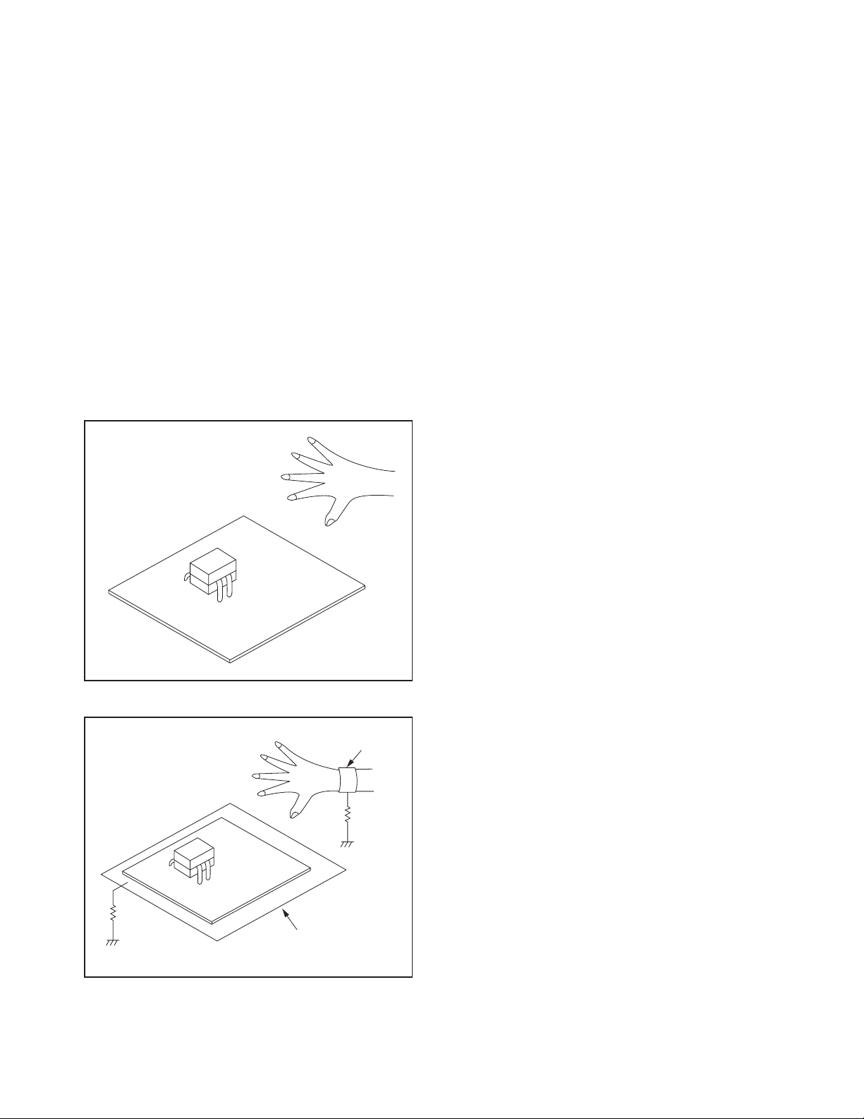
Instructions for Handling Semi-
conductors
Electrostatic breakdown of the semi-conductors may
occur due to a potential difference caused by
electrostatic charge during unpacking or repair work.
1. Ground for Human Body
Be sure to wear a grounding band (1 MΩ) that is
properly grounded to remove any static electricity that
may be charged on the body.
2. Ground for Workbench
Be sure to place a conductive sheet or copper plate
with proper grounding (1 MΩ) on the workbench or
other surface, where the semi-conductors are to be
placed. Because the static electricity charge on
clothing will not escape through the body grounding
band, be careful to avoid contacting semi-conductors
with your clothing.
<Incorrect>
CBA
Grounding Band
Conductive Sheet or
Copper Plate
1MΩ
1MΩ
<Correct>
CBA
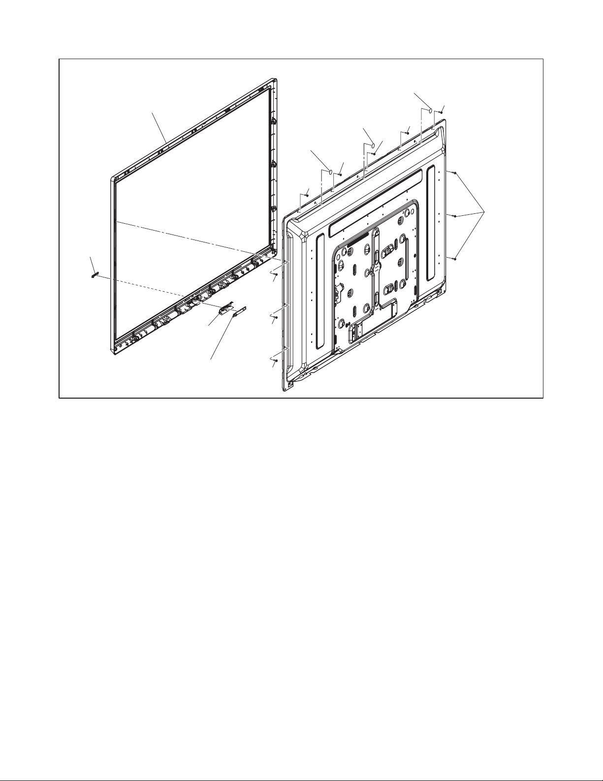
4-1 FL13.16-A_DC
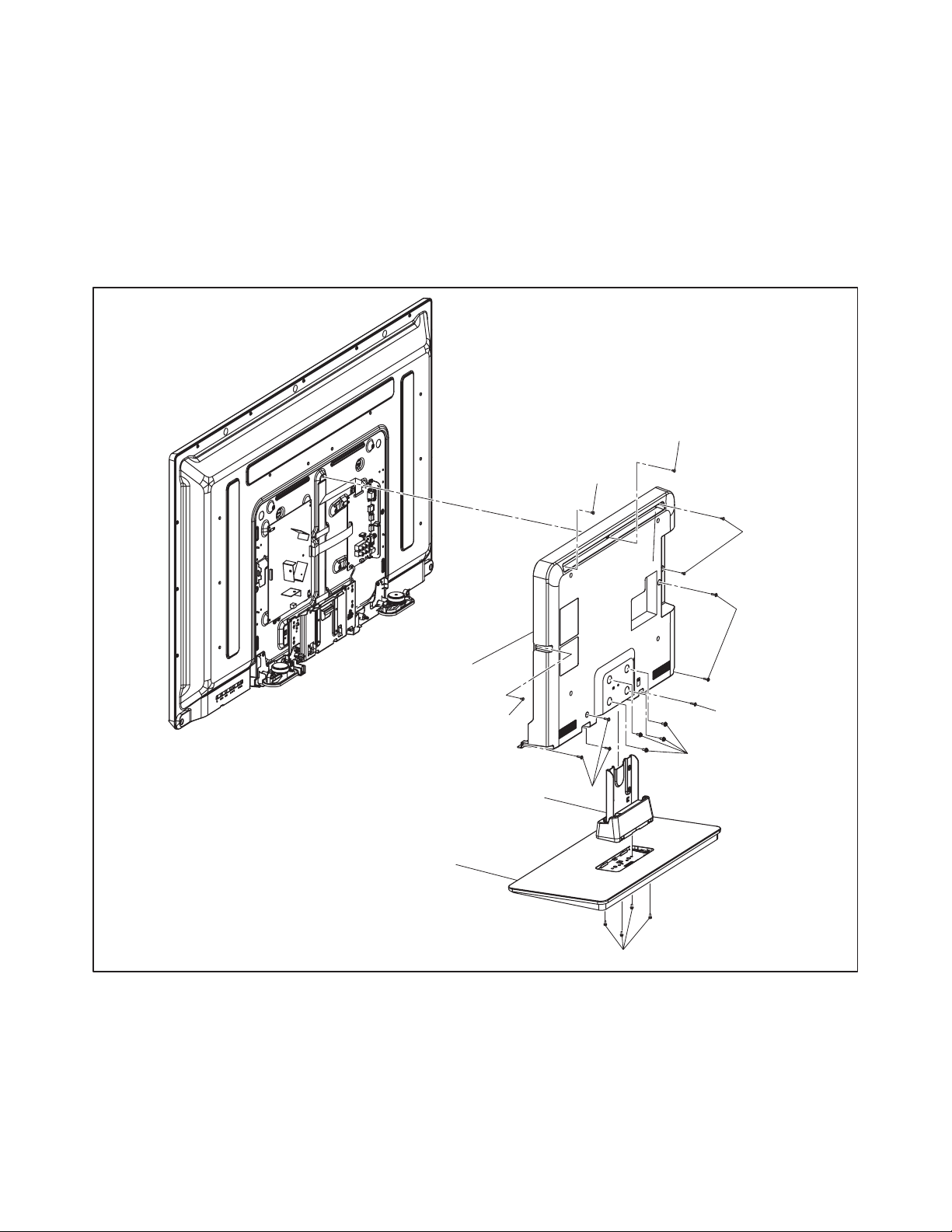
CABINET DISASSEMBLY INSTRUCTIONS
1. Disassembly Flowchart
This flowchart indicates the disassembly steps for the
cabinet parts and the CBA in order to gain access to
items to be serviced. When reassembling, follow the
steps in reverse order. Bend, route and dress the
cables as they were.
2. Disassembly Method
Note:
(1) Order of steps in procedure. When reassembling,
follow the steps in reverse order. These numbers
are also used as the Identification (location) No. of
parts in figures.
(2) Parts to be removed or installed.
(3) Fig. No. showing procedure of part location
(4) Identification of parts to be removed, unhooked,
unlocked, released, unplugged, unclamped, or
desoldered.
P = Spring, L = Locking Tab, S = Screw,
H = Hex Screw, CN = Connector
e.g. 2(S-2) = two Screws of (S-2),
2(L-2) = two Locking Tabs of (L-2)
(5) Refer to the following “Reference Notes in the
Ta bl e .”
Precautions concerning the LCD Panel
Assembly:
1. When you disassemble/re-assemble the Front
Cabinet
• Do not pull the FFC Cable and Board Cable
forcefully when you re-assemble.
• Be careful not to scratch the display panel when
assembling.
• The screw tightening torque must be 6kgf·cm
(5.2lb·in).
• Make sure to replace the Sensor Lens to a new one
when replacing the Front Cabinet.
• Be careful not to scratch the rear frame when
disassembling/re-assembling or when tightening the
screws.
Step/
Loc.
No.
Part
Fig.
No.
Removal Note
[1]
Stand
Hinge
Assembly
D1 4(S-1), 4(S-2) ---
[2]
Stand Base
Assembly
D1 --------------- ---
[3] Rear Cover D1 5(S-3), 6(S-4) ---
[4]
Power
Supply
CBA
D2
D5
4(S-5), CN501,
CN601, CN1001
---
[5]
Digital Main
CBA Unit
D2
D5
4(S-6), CN3013,
CN3101, CN3801,
Jack Holder
---
[6] Speaker D3 --------------- ---
[7]
Bottom
Cover L
D3 2(S-7), (S-8) ---
[8]
Bottom
Cover R
D3
2(S-9), (S-10),
Function Knob
---
[1] Stand Hinge
Assembly
[3] Rear Cover
[9] Function
CBA Unit
[10] Stand Bracket
[11] LCD Panel
Assembly
[6] Speaker
[13] Front Cabinet
[2] Stand Base
Assembly
[4] Power Supply
CBA
[7] Bottom
Cover L
[8] Bottom
Cover R
[12] IR Sensor
CBA Unit
[5] Digital Main
CBA Unit
[9]
Function
CBA Unit
D3
D5
CN4001 2
[10]
Stand
Bracket
D3 4(S-11) ---
[11]
LCD Panel
Assembly
D3 --------------- ---
[12]
IR Sensor
CBA Unit
D4 Sensor Plate 2
[13]
Front
Cabinet
D4
11(S-12), Blind Label,
Sensor Lens
1
↓
(1)
↓
(2)
↓
(3)
↓
(4)
↓
(5)
Step/
Loc.
No.
Part
Fig.
No.
Removal Note
4-2 FL13.16-A_DC
2. When you disassemble/re-assemble the
Function CBA Unit or the IR Sensor CBA Unit
• Be careful not to break the hooks. If you pull with too
much force, the hooks may be damaged.
• Make sure the hooks are securely in place when
assembling.
• The Function CBA Unit and Function Knob are fixed
in place by the hooks. Make sure these hooks are
not damaged. Make sure the Function CBA Unit and
Function Knob are securely in place when re-
assembling.
• The IR Sensor CBA Unit and Sensor Plate are fixed
in place by the hooks. Make sure these hooks are
not damaged. Make sure the IR Sensor CBA Unit
and Sensor Plate are securely in place when re-
assembling.
• When assembling the IR Sensor CBA Unit, make
sure the Sensor Plate is properly set so that it
contacts the LCD Panel Assembly.
[3] Rear Cover
(S-3)
(S-3)
(S-3)
(S-3)
(S-2)
(S-1)
(S-4)
(S-4)
(S-4)
[1] Stand Hinge Assembly
[2] Stand Base Assembly
Fig. D1
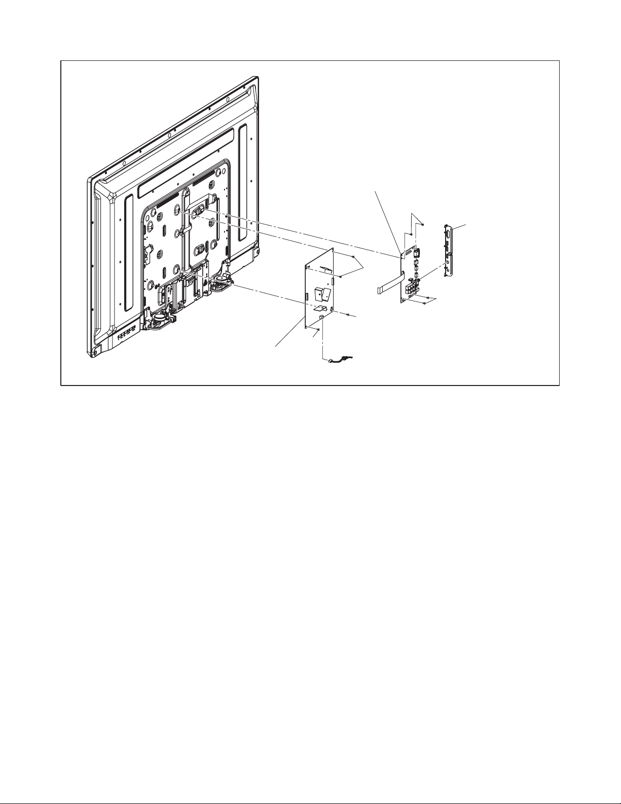
4-3 FL13.16-A_DC
[5] Digital Main CBA Unit
[4] Power Supply CBA
(S-6)
(S-6)
Jack Holder
(S-5)
(S-5)
(S-5)
Fig. D2

4-4 FL13.16-A_DC
[6] Speaker
[6] Speaker
[10] Stand Bracket
[7] Bottom Cover L
[8] Bottom Cover R
[9] Function CBA Unit
*
2
[11] LCD Panel Assembly
(S-11)
(S-11)
Function Knob
(S-7)
(S-9)
(S-10)
(S-8)
Fig. D3
*
2
: Make sure to read all the precautions on page 4-2 when you disassemble/re-assemble the
Function CBA Unit.
4-5 FL13.16-A_DC
[12] IR Sensor CBA Unit
*
2
Sensor Plate
Blind Label
Blind Label
Blind Label
[13] Front Cabinet
*
1
(S-12)
(S-12)
(S-12)
(S-12)
(S-12)
(S-12)
(S-12)
(S-12)
(S-12)
Sensor
Lens
Fig. D4
*
1
: Make sure to read all the precautions on page 4-1 when you disassemble/re-assemble the
Front Cabinet.
*
2
: Make sure to read all the precautions on page 4-2 when you disassemble/re-assemble the IR
Sensor CBA Unit.
4-6 FL13.16-A_DC
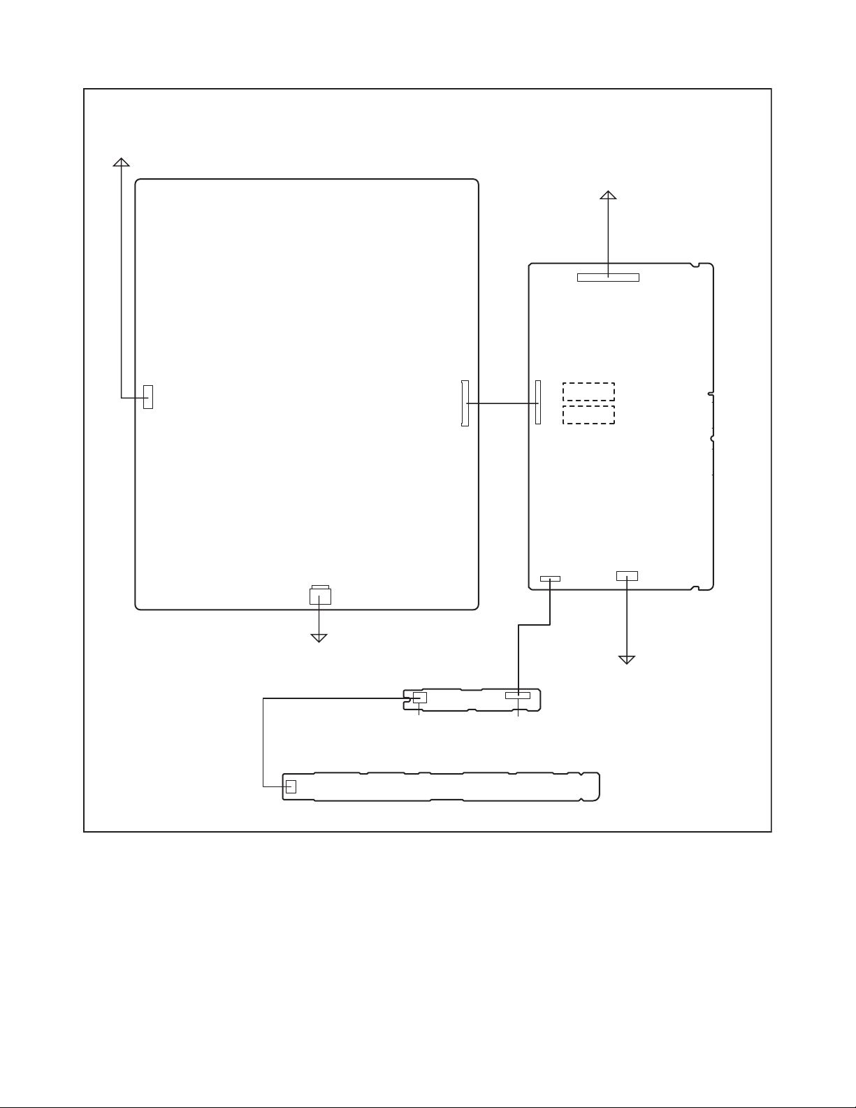
TV Cable Wiring Diagram
Power Supply CBA
Function CBA Unit
IR Sensor CBA Unit
To LCD Panel
Assembly
To LCD Panel
Assembly
To AC Cord
To Speaker
Digital Main
CBA Unit
CN3801
CN4001
CN4051 CN4052
CN1001
CN601
CN501
CN3013
CN3101
CN3701
CN3602
*1
*2
Fig. D5
*1: TYPE A
*2: TYPE B
5-1 FL13.16EA
ELECTRICAL ADJUSTMENT INSTRUCTIONS
General Note: “CBA” is abbreviation for
“Circuit Board Assembly.”
Note: Electrical adjustments are required after
replacing circuit components and certain
mechanical parts. It is important to perform
these adjustments only after all repairs and
replacements have been completed.
Also, do not attempt these adjustments unless
the proper equipment is available.
Test Equipment Required
1. Remote control unit
2. Color Analyzer,
CA-310 (KONICA MINOLTA Luminance meter) or
measuring instrument as good as CA-310.
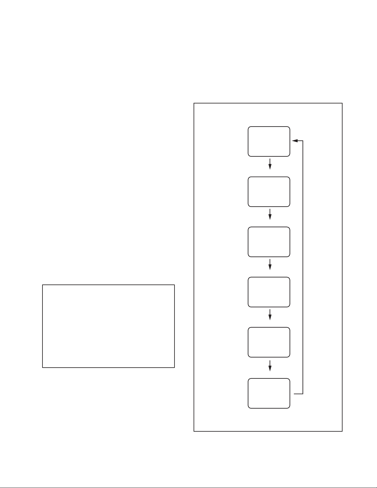
How to set up the service mode:
Service mode:
1. Turn the power on.
2. Press [MENU] button to display Setup menu.
3. Select “Features”.
4. Select “Software Upgrade”.
5. Select “Current Software Info”.
6. Press [0], [4], [2], [5], [7], [4] and [INFO] buttons on
the remote control unit in this order. The following
screen appears.
1. Purity Check Mode
This mode cycles through full-screen displays of red,
green, blue, and white to check for non-active pixels.
1. Enter the service mode.
2. Each time the [7] button on the remote control unit
is pressed, the display changes as follows.
3. To cancel or to exit from the Purity Check Mode,
press [CH RETURN] or [PREV CH] button.
Code:
Pic code:
Panel-Option code:
MIPS:
Press "POWER" key to exit.
*******-**-**-****-**
**-***-**-*****-***
**-***-***-***-***
**
Safety:
HDMI EDID:
HDMI UART:
Touch Sensor Ver:
Safety_Non
**
OFF
-.-- / ---
Total Watch Time:
Lightsensor:
*****
**
"
*
" differs depending on the models.
[7] button
Note:
When entering this mode, the default setting is White mode.
Purity Check Mode
[7] button
White 50% mode
Red, Green, Blue mode
V-ramp mode
Black mode
[7] button
White mode
[7] button
[7] button
White 20% mode
[7] button

5-2 FL13.16EA
The White Balance Adjustment should be
performed when replacing the LCD Panel
or Digital Main CBA.
2. White Balance Adjustment
Purpose: To mix red and blue beams correctly for
pure white.
Symptom of Misadjustment: White becomes bluish
or reddish.
1. Operate the unit for more than 60 minutes.
2. Enter the service mode.
3. Press [VOLUME DOWN] button three times on the
remote control unit to select “Drive setting” mode.
“Drive” appears in the screen.
4. Set the color analyzer at the CHROMA mode and
zero point calibration. Bring the optical receptor
pointing at the center of the LCD-Panel.
Note: The optical receptor must be set
perpendicularly to the LCD Panel surface.
5. Press [3] button to select the “HDB” for High Drive
Blue adjustment. (“HDB” appears in the screen.)
6. Press [MENU] button. The internal Raster signal
appears in the screen. (“Internal (Single)” appears
in the upper right of the screen as shown below.)
7. Press [CHANNEL UP/DOWN] buttons to adjust
the color temperature becomes 12000°K
(x
=
0.272 / y
=
0.278 ± 0.003).
8. Press [1] button to select the “HDR” for High Drive
Red adjustment (“HDR” appears in the screen.)
and press [CHANNEL UP/DOWN] buttons to
adjust the color temperature.
9. If necessary, adjust the “HDB” or “HDR” again.
10. Press [6] button to select the “LDB” for Low Drive
Blue adjustment (“LDB” appears in the screen.)
and press [CHANNEL UP/DOWN] buttons to
adjust the color temperature.
11. Press [4] button to select the “LDR” for Low Drive
Red adjustment (“LDR” appears in the screen.)
and press [CHANNEL UP/DOWN] buttons to
adjust the color temperature.
12. If necessary, adjust the “LDB” or “LDR” again.
13. Press [VOLUME DOWN] button to shift to the
“Debugging Message” mode.
If there is no message under “[WB]” section, this
adjustment completes.
If “Drive settings are NG. Retry again.” is
displayed, repeat above steps from 5. to 12. Then
check “Debugging Message” again. If “Drive
settings are NG. Retry again.” is displayed, replace
the LCD Panel or Digital Main CBA.
14. To cancel or to exit from the White Balance
Adjustment, press [CH RETURN] or [PREV CH]
button.
ITEM
SPECIFICATION
Color temperature
x= 0.272 ± 0.003
y= 0.278 ± 0.003
Input Signal
Internal pattern
(40/80% raster)
Measurement point Screen center
M. EQ.
CA-310 (KONICA MINOLTA
Luminance meter) or
measuring instrument as
good as CA-310.
Aging time
60min.
(Retail MODE/100IRE Raster
HDMI 1080i@60)
MODE setting of TV
Shipment setting/
Retail MODE
Ambient
temperature
25°C ± 5°C
Color Analyzer
Perpendicularity
To avoid interference from ambient
light, this adjustment should be
performed in a dark room.
Internal (Single)
HDB 0
Internal (Single)
LDB 0

6-1 FL13.16INT
HOW TO INITIALIZE THE LCD TV
The purpose of initialization is to place the set in a new out of box condition. The customer will be prompted to
select a language and program channels after the set has been initialized.
To put the program back at the factory-default, initialize the LCD TV using the following procedure.
1. Turn the power on.
2. Enter the service mode.
- To cancel the service mode, press [ ] button on
the remote control unit.
3. Press [BACK] button to enter the Control Panel
Key Confirmation Menu.
4. Press any button on the control panel.
5. Press [INFO] button to proceed with the self check
mode.
6. Make sure to confirm the "INITIALIZED FINISH"
appears in the green screen.
7. Unplug the AC Cord and plug it back on again.

7-1 FL13.16FW
FIRMWARE RENEWAL MODE
Equipment Required
a. USB storage device
b. Remote Control Unit
Firmware Update Procedure
User Upgrade (Filename example: TVNB012_00_UF_XX91_BC.ecc or TVNB1012_00_UG_XX91_BA0.bin)
Upgrade the firmware only. The setting values will not be initialized.
The User Upgrade and the Firmware Upgrade (Factory Upgrade) will be done by the same file. If you want to
upgrade the firmware and initialize the setting values also, add “FACT_” at the beginning of the filename.
If you want to upgrade the firmware only and leave the setting values as they are, eliminate the “FACT_” from the
filename.
Update procedure
1. Turn the power on.
2. Press [MENU] button to display Menu.
3. Select “Features”.
4. Select “Software Upgrade”.
5. Select “Upgrade” to display Upgrade screen.
6. Press [OK] button to display Software Upgrade
screen.
7. Select “USB” and press [OK] button.
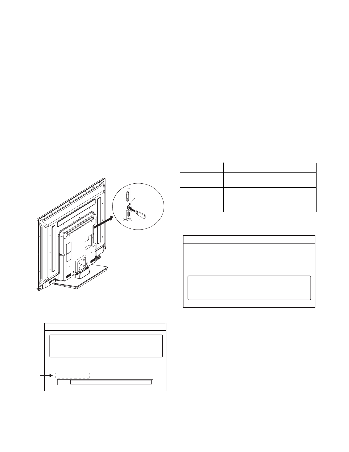
8. Insert the USB storage device to the USB port as
shown below.
9. Select “Check” and press [OK] button.
10. Select “Upgrade” and press [OK] button to start
software upgrade.
11. The update will start and the following will appear
in the screen.
Note: If the above screen isn’t displayed, repeat from
step 1.
The appearance shown in *1 is described as follows.
12. When the firmware update is completed, the
following will appear in the screen.
Remove the USB storage device from the USB
port.
Turn the power off and turn the power on again.
USB port
USB storage
device
Rear Cabinet
Appearance State
Downloading...
Downloading the firmware from
the USB storage device.
Writing...
Writing the downloaded firmware
in flash memory.
Checking... Checking the new firmware.
Software upgrade in progress. Please wait.
Do not remove the USB storage device or
turn the TV off while upgrade is in progress.
Software Upgrade
Downloading...
Current Version:
New Version:
*******-***-*-***-****
*******-***-*-***-****
0%
*1
"
*
" differs depending on the models.
Software Upgrade
The software upgrade is completed.
Remove USB storage device, turn TV off then on again.
7-2 FL13.16FW
Factory Upgrade (Firmware Upgrade/Flash Upgrade)
Firmware Upgrade
(Filename example: FACT_TVNB012_00_UF_XX91_BC.ecc or FACT_TVNB1012_00_UG_XX91_BA0.bin)
Upgrade the firmware and initialize the setting values.
The User Upgrade and the Firmware Upgrade (Factory Upgrade) will be done by the same file. If you want to
upgrade the firmware and initialize the setting values also, add “FACT_” at the beginning of the filename.
If you want to upgrade the firmware only and leave the setting values as they are, eliminate the “FACT_” from the
filename.
Flash Upgrade
(Filename example: ALL_TVNB012_00_UF_XX91_BC.ecc or ALL_TVNB1012_00_UG_XX91_BA0.bin)
Upgrade the firmware and initialize the setting values along with the factory default such as White Balance, etc.
Before the upgrade, you will need to make a note of all the factory default so you will be able to set it back on the
TV after the initialization.
The Flash Upgrade will be done by it's unique file.
The User Upgrade/Firmware Upgrade (Factory Upgrade) file cannot be used for this upgrade.
Update procedure
1. Turn the power off.
2. Insert the USB storage device to the USB port as
shown below.
3. Turn the power on.
4. The update will start and the following will appear
in the screen.
Note: If the above screen isn’t displayed, repeat from
step 1.
The appearance shown in *1 is described as follows.
5. When the firmware update is completed, the
following will appear in the screen.
Remove the USB storage device from the USB
port.
Turn the power off and turn the power on again.
Service mode initial screen with a word
“INITIALIZED” will appear in the screen. The color
of the word “INITIALIZED” will change from red to
green when initialization is completed.
USB port
USB storage
device
Rear Cabinet
Software upgrade in progress. Please wait.
Do not remove the USB storage device or
turn the TV off while upgrade is in progress.
Software Upgrade
Downloading...
Current Version:
New Version:
*******-***-*-***-****
*******-***-*-***-****
0%
*1
"
*
" differs depending on the models.
Appearance State
Downloading...
Downloading the firmware from
the USB storage device.
Writing...
Writing the downloaded firmware
in flash memory.
Checking... Checking the new firmware.
Software Upgrade
The software upgrade is completed.
Remove USB storage device, turn TV off then on again.
Loading...