


 Loading...
ORDER NO.KMF1107371CE
Multi-Function printer
Model No. KX-MB1500UCB
(for Ukraine, Kazakhstan)
© Panasonic System Networks Co., Ltd. 2011 Unauthorized copying and distribution is a violation of law.

KX-MB1500UCB
TABLE OF CONTENTS
|
PAGE |
|
1 Safety Precautions ----------------------------------------------- |
|
5 |
1.1. For Service Technicians ---------------------------------- |
|
5 |
1.2. AC Caution--------------------------------------------------- |
|
5 |
1.3. Personal Safety Precautions ---------------------------- |
|
6 |
1.3.1. Moving Sections of the Unit------------------------- |
6 |
|
1.3.2. Live Electrical Sections ------------------------------ |
|
6 |
1.4. Service Precautions --------------------------------------- |
|
6 |
1.4.1. Precautions to Prevent |
Damage from |
|
Static Electricity ---------------------------------------- |
|
6 |
2 Warning -------------------------------------------------------------- |
|
7 |
2.1. About Lead Free Solder (PbF: Pb free) -------------- |
7 |
|
2.1.1. Suggested PbF Solder ------------------------------- |
|
7 |
2.2. Discarding of P. C. Board -------------------------------- |
|
8 |
2.3. Insulation Resistance Test ------------------------------- |
|
8 |
2.4. Battery Caution --------------------------------------------- |
|
8 |
2.5. Laser Beam and Fuser Unit Section ------------------ |
8 |
|
2.6. Note for Repairing------------------------------------------ |
|
9 |
3 Specifications ---------------------------------------------------- |
|
10 |
4 General/Introduction------------------------------------------- |
|
11 |
4.1. Optional Accessories------------------------------------ |
|
11 |
4.2. Translation Lists ------------------------------------------ |
|
11 |
4.2.1. Error Message (Display)--------------------------- |
|
11 |
5 Features------------------------------------------------------------ |
|
12 |
5.1. General Features----------------------------------------- |
|
12 |
5.2. Hardware Requirements for |
Multi-Function |
|
Software ---------------------------------------------------- |
|
12 |
6 Technical Descriptions---------------------------------------- |
|
13 |
6.1. Connection Diagram------------------------------------- |
|
13 |
6.2. General Block Diagram--------------------------------- |
|
14 |
6.3. Main Board Section-------------------------------------- |
|
16 |
6.3.1. Data Flow---------------------------------------------- |
|
16 |
6.4. CIS Control Section-------------------------------------- |
|
24 |
6.5. Motor Drive Section-------------------------------------- |
|
26 |
6.5.1. Engine Motor Control Circuit --------------------- |
26 |
|
6.5.2. FB (Flat bed) motor drive circuit ----------------- |
29 |
|
6.6. Timing chart and wave form of scanner |
|
|
motors------------------------------------------------------- |
|
31 |
6.6.1. Drive mode of FB motor --------------------------- |
|
31 |
6.6.2. Normal 1-2 phase excitation (half step)-------- |
32 |
|
6.6.3. W1-2 phase excitation (Quarter step) ---------- |
33 |
|
6.6.4. W1-2 phase excitation (Quarter step) ---------- |
34 |
|
6.7. FAN Motor Section--------------------------------------- |
|
35 |
6.7.1. General ------------------------------------------------ |
|
35 |
6.7.2. Circuit Diagram of FAN ---------------------------- |
|
35 |
6.7.3. Speed Control Block -------------------------------- |
|
35 |
6.7.4. Abnormal detect and Lock protect Block ------ |
38 |
|
6.8. Solenoid Driver Section -------------------------------- |
|
39 |
6.9. LSU (Laser Scanning Unit) Section ----------------- |
40 |
|
6.10. Sensors and Switches Section |
----------------------- |
42 |
6.10.1. Pick up & Registration & Manual paper |
|
|
sensor ------------------------------------------------- |
|
43 |
6.10.2. Print timing sensor ---------------------------------- |
|
43 |
6.10.3. Exit sensor -------------------------------------------- |
|
44 |
6.10.4. Interlock switch--------------------------------------- |
|
44 |
6.10.5. Toner Sensor ----------------------------------------- |
|
45 |
6.10.6. Drum Life sensor circuit---------------------------- |
|
46 |
6.11. Operation Board Section ------------------------------- |
|
47 |
6.12. LCD Section ----------------------------------------------- |
|
48 |
PAGE |
|
6.13. HVPS (High Voltage Power Supply) Section ----- |
49 |
6.13.1. HVPS Specification for EUK1MNB31HA------ |
49 |
6.13.2. CHG-BIAS (Charge BIAS)/UNIT ---------------- |
49 |
6.13.3. DEV DC BIAS UNIT-------------------------------- |
50 |
6.13.4. DEV AC BIAS UNIT -------------------------------- |
50 |
6.13.5. TRA (-) BIAS (Transfer (-) BIAS)/TRA (+) |
|
BIAS (Transfer (+) BIAS) UNIT------------------ |
50 |
6.14. Heat Lamp Control Circuit----------------------------- |
51 |
6.15. Main Board Power Supply Section------------------ |
56 |
6.15.1. 3.3V and 1.2V Power Supply Descriptions --- |
56 |
6.15.2. +5VD Power Supply Descriptions -------------- |
57 |
6.16. Power Supply Board Section ------------------------- |
59 |
6.17. Mechanical Operation ---------------------------------- |
60 |
6.17.1. Printing ------------------------------------------------ |
60 |
7 Location of Controls and Components ----------------- |
61 |
7.1. Overview--------------------------------------------------- |
61 |
7.1.1. Front view--------------------------------------------- |
61 |
7.1.2. Rear view --------------------------------------------- |
61 |
7.2. Control Panel --------------------------------------------- |
62 |
8 Installation Instructions -------------------------------------- |
63 |
8.1. Installation ------------------------------------------------- |
63 |
8.1.1. Installation Space ----------------------------------- |
63 |
8.1.2. Recording Paper ----------------------------------- |
64 |
8.1.3. Documents the Unit Can Send ------------------ |
68 |
8.1.4. Toner Cartridge -------------------------------------- |
68 |
8.1.5. Required computer environment---------------- |
71 |
8.1.6.Installing Multi-Function Station on a
computer ---------------------------------------------- |
72 |
8.2. Connections----------------------------------------------- |
73 |
9 Test Mode --------------------------------------------------------- |
74 |
9.1. Test Functions -------------------------------------------- |
74 |
9.1.1. Button Code Table ---------------------------------- |
75 |
9.1.2. Print Test Pattern------------------------------------ |
76 |
10 Service Mode----------------------------------------------------- |
77 |
10.1. Programming and Lists--------------------------------- |
77 |
10.1.1. Operation --------------------------------------------- |
77 |
10.1.2. Operation Flow -------------------------------------- |
77 |
10.1.3. Service Function Table ---------------------------- |
78 |
10.1.4. Memory Clear Specification ---------------------- |
78 |
10.2. User Mode (The list below is an example of |
|
the SYSTEM SETUP LIST the unit prints out.) -- |
79 |
10.3. History (Example of a printed out list) -------------- |
80 |
10.3.1. Descriptions of The History Report------------- |
81 |
11 Troubleshooting Guide --------------------------------------- |
82 |
11.1. User Recoverable Errors ------------------------------ |
82 |
11.1.1. Program Mode Table------------------------------- |
84 |
11.2. Troubleshooting Details -------------------------------- |
86 |
11.2.1. Outline ------------------------------------------------- |
86 |
11.2.2. Starting Troubleshooting -------------------------- |
86 |
11.2.3. Initialization ------------------------------------------- |
87 |
11.2.4. Simple Check List----------------------------------- |
88 |
11.2.5. Simplified Troubleshooting Guide--------------- |
89 |
11.2.6. CALL SERVICE Troubleshooting Guide ------ |
92 |
11.2.7. Print ---------------------------------------------------- |
98 |
11.2.8. Recording Paper Feed --------------------------- |
104 |
11.2.9. Copy and FAX -------------------------------------- |
111 |
11.2.10. Initializing Error ------------------------------------- |
113 |
11.2.11. Operation Panel Section ------------------------- |
114 |
2

KX-MB1500UCB
11.2.12. Sensor Section ------------------------------------- |
114 |
14.4.2. Removal Procedure ------------------------------ |
|
|
174 |
||
11.2.13. Motor Section --------------------------------------- |
116 |
14.4.3. Procedure ------------------------------------------- |
|
|
|
175 |
|
11.2.14. LSU Section----------------------------------------- |
118 |
14.4.4. Removing Solder From Between Pins ------- |
175 |
||||
11.2.15. CIS Control Section ------------------------------- |
119 |
14.5. Main Board Section------------------------------------ |
|
|
|
176 |
|
11.2.16. High Voltage Value Check Point --------------- |
121 |
14.5.1. NG Example ---------------------------------------- |
|
|
|
177 |
|
11.2.17. High Voltage Section------------------------------ |
123 |
14.6. Test Chart |
------------------------------------------------ |
|
|
|
178 |
11.2.18. USB Section ---------------------------------------- |
128 |
14.6.1. ITU-T No.1 Test Chart---------------------------- |
|
|
178 |
||
11.2.19. Main Board Section ------------------------------- |
133 |
14.6.2. ITU-T No.2 Test Chart---------------------------- |
|
|
179 |
||
11.2.20. Power Supply Board Section ------------------- |
134 |
15 Schematic Diagram ------------------------------------------ |
|
|
|
181 |
|
11.3. Recording Paper Jam --------------------------------- |
137 |
15.1. For Schematic Diagram ------------------------------ |
|
|
181 |
||
11.3.1. When the recording paper has jammed |
|
15.2. Main Board ---------------------------------------------- |
|
|
|
182 |
|
inside of the unit------------------------------------ |
137 |
15.2.1. Main Board (1) ------------------------------------- |
|
|
|
182 |
|
11.3.2. When the recording paper is not fed into |
|
15.2.2. Main Board (2) ------------------------------------- |
|
|
|
186 |
|
the unit properly ------------------------------------ |
140 |
15.3. Sensor Board ------------------------------------------- |
|
|
|
188 |
|
11.3.3. When the recording paper in the manual |
|
15.3.1. Operation Board ----------------------------------- |
|
|
|
188 |
|
input tray is not fed into the unit properly ---- |
141 |
15.3.2. Sensor Board--------------------------------------- |
|
|
|
189 |
|
12 Service Fixture & Tools-------------------------------------- |
142 |
15.4. High Voltage Power Supply Board----------------- |
|
190 |
|||
13 Disassembly and Assembly Instructions ------------- |
143 |
15.5. Low Voltage Power Supply Board ----------------- |
|
191 |
|||
13.1. Flow Chart for Disassembly-------------------------- |
144 |
16 Printed Circuit Board ---------------------------------------- |
|
|
|
193 |
|
13.2. How to Remove Rear Cover------------------------- |
145 |
16.1. Main Board ---------------------------------------------- |
|
|
|
193 |
|
13.3. How to Remove Front Cover ----------------------- |
145 |
16.1.1. Main Board: Component View ----------------- |
|
193 |
|||
13.4. How to Remove Right Cover ------------------------ |
146 |
16.1.2. Main Board: Bottom View ----------------------- |
|
|
194 |
||
13.5. How to Remove Left Cover -------------------------- |
147 |
16.2. Sensor Board ------------------------------------------- |
|
|
|
195 |
|
13.6. How to Remove FB Unit ------------------------------ |
148 |
16.2.1. Operation Board ----------------------------------- |
|
|
|
195 |
|
13.7. How to Remove Upper Cabinet Cover------------ |
149 |
16.2.2. Interlock Board------------------------------------- |
|
|
|
196 |
|
13.8. How to Remove Bottom Plate----------------------- |
150 |
16.2.3. Gear Board ----------------------------------------- |
|
|
|
196 |
|
13.9. How to Remove Power Board Unit----------------- |
151 |
16.2.4. Toner Sensor Board ------------------------------ |
|
|
196 |
||
13.10. How to Remove Fuser Unit -------------------------- |
152 |
16.2.5. Fuser Board ---------------------------------------- |
|
|
|
197 |
|
13.11. How to Remove Fan, HVPS and Inter-lock |
|
16.3. High Voltage Power Supply Board----------------- |
|
198 |
|||
Board ------------------------------------------------------ |
152 |
16.3.1. High |
Voltage |
Power |
Supply |
Board: |
|
13.12. How to Remove Main Board and Shield Cover - 153 |
Component View ---------------------------------- |
|
|
198 |
|||
13.13. How to Remove Drive Unit --------------------------- |
153 |
16.3.2. High Voltage Power Supply Board: Bottom |
|
||||
13.14. How to Remove Clutch Gear Cover --------------- |
154 |
View--------------------------------------------------- |
|
|
|
|
198 |
13.15. How to Remove Pick-up Roller --------------------- |
155 |
16.4. Low Voltage Power Supply Board ----------------- |
|
199 |
|||
13.16. How to Remove Operation Panel Unit ------------ |
156 |
16.4.1. Low |
Voltage |
Power |
Supply |
Board: |
|
13.17. How to Disassemble FB Unit ------------------------ |
157 |
Component View ---------------------------------- |
|
|
199 |
||
13.18. How to Remove LSU and Glasses----------------- |
158 |
16.4.2. Low Voltage Power Supply Board: Bottom |
|
||||
13.19. Installation Position of The Lead-------------------- |
159 |
View--------------------------------------------------- |
|
|
|
|
199 |
13.19.1. Main cabinet section ------------------------------ |
159 |
17 Exploded View and Replacement Parts List --------- |
200 |
||||
13.19.2. Side cabinet section(1) --------------------------- |
160 |
17.1. General Section ---------------------------------------- |
|
|
|
201 |
|
13.19.3. Side cabinet section (2) -------------------------- |
161 |
17.1.1. Operation Panel Section ------------------------ |
|
|
202 |
||
13.19.4. Side cabinet section (3) -------------------------- |
162 |
17.1.2. Top Cover Section (1) --------------------------- |
|
|
204 |
||
13.19.5. Side cabinet section (4) -------------------------- |
163 |
17.1.3. Top Cover Section (2) ---------------------------- |
|
|
206 |
||
13.19.6. Fuser section --------------------------------------- |
164 |
17.1.4. Top Cover Section (3) ---------------------------- |
|
|
208 |
||
13.19.7. Power supply unit section ----------------------- |
165 |
17.1.5. Top Cover Section (4) ---------------------------- |
|
|
210 |
||
14 Maintenance----------------------------------------------------- |
166 |
17.1.6. Fuser Section -------------------------------------- |
|
|
|
212 |
|
14.1. Maintenance Items and Component Locations - 166 |
17.1.7. Main Cabinet Section (1) ------------------------ |
|
|
214 |
|||
14.1.1. Outline ------------------------------------------------ |
166 |
17.1.8. Main Cabinet Section (2) ------------------------ |
|
|
216 |
||
14.1.2. Maintenance Check Items/Component |
|
17.1.9. Main Cabinet Section (3) ------------------------ |
|
|
218 |
||
Locations--------------------------------------------- |
166 |
17.1.10. Main Cabinet Section (4) ------------------------ |
|
|
220 |
||
14.2. Maintenance --------------------------------------------- |
168 |
17.1.11. Left-side Cabinet Section(1)-------------------- |
|
222 |
|||
14.2.1. Cleaning the White Plates and Glass--------- |
168 |
17.1.12. Left-side Cabinet Section(2)-------------------- |
|
224 |
|||
14.3. Printing Operation Principle-------------------------- |
169 |
17.1.13. Left-side Cabinet Section(3)-------------------- |
|
226 |
|||
14.3.1. Process Chart and Process BIAS ------------- |
169 |
17.1.14. Power Supply Unit Section --------------------- |
|
228 |
|||
14.3.2. Charging --------------------------------------------- |
169 |
17.1.15. Base Cassette Section--------------------------- |
|
|
230 |
||
14.3.3. Exposing --------------------------------------------- |
170 |
17.1.16. Main Unit Section (1) ----------------------------- |
|
|
232 |
||
14.3.4. Developing and Transcription------------------- |
171 |
17.1.17. Main Unit Section (2) ----------------------------- |
|
|
234 |
||
14.3.5. Cleaning of Transfer Roller---------------------- |
172 |
17.1.18. Actual Size of Screws and Washer ----------- |
|
236 |
|||
14.3.6. Fixing ------------------------------------------------- |
173 |
17.1.19. Accessories and Packing Materials ---------- |
|
238 |
|||
14.4. How to Replace the Flat Package IC-------------- |
174 |
17.2. Electrical Parts List ------------------------------------ |
|
|
|
240 |
|
14.4.1. Preparation ------------------------------------------ |
174 |
17.2.1. Main Board------------------------------------------ |
|
|
|
240 |
|
3

KX-MB1500UCB |
|
17.2.2. Sensor Board--------------------------------------- |
243 |
17.2.3. High Voltage Power Supply Board ------------ |
244 |
17.2.4. Low Voltage Power Supply Board------------- |
244 |
4

KX-MB1500UCB
1Safety Precautions
1.Before servicing, unplug the AC power cord to prevent an electric shock.
2.When replacing parts, use only the manufacturer's recommended components.
3.Check the condition of the power cord. Replace if wear or damage is evident.
4.After servicing, be sure to restore the lead dress, insulation barriers, insulation papers, shields, etc.
5.Before returning the serviced equipment to the customer, be sure to perform the following insulation resistance test to prevent the customer from being exposed to shock hazards.
1.1.For Service Technicians
•Repair service shall be provided in accordance with repair technology information such as service manual so as to prevent fires, injury or electric shock, which can be caused by improper repair work.
1.When repair services are provided, neither the products nor their parts or members shall be remodeled.
2.If a lead wire assembly is supplied as a repair part, the lead wire assembly shall be replaced.
3.FASTON terminals shall be plugged straight in and unplugged straight out.
•ICs and LSIs are vulnerable to static electricity.
When repairing, the following precautions will help prevent recurring malfunctions.
1.Cover the plastic part's boxes with aluminum foil.
2.Ground the soldering irons.
3.Use a conductive mat on the worktable.
4.Do not touch the IC or LSI pins with bare fingers.
1.2.AC Caution
For safety, before closing the lower cabinet, please make sure of the following precautions.
1.The earth lead is fixed with the screw.
2.The AC connector is connected properly.
5

KX-MB1500UCB
1.3.Personal Safety Precautions
1.3.1.Moving Sections of the Unit
Be careful not to let your hair, clothes, fingers, accessories, etc., become caught in any moving sections of the unit.
The moving sections of the unit are the rollers and a gear. There is a separation roller and a document feed roller which are rotated by the document feed motor. A gear rotates the two rollers. Be careful not to touch them with your hands, especially when the unit is operating.
1.3.2.Live Electrical Sections
All the electrical sections of the unit supplied with AC power by the AC power cord are live. Never disassemble the unit for service with the AC power supply plugged in.
CAUTION:
AC voltage is supplied to the primary side of the power supply unit. Therefore, always unplug the AC power cord before disassembling for service.
1.4.Service Precautions
1.4.1.Precautions to Prevent Damage from Static Electricity
Electrical charges accumulate on a person. For instance, clothes rubbing together can damage electric elements or change their electrical characteristics. In order to prevent static electricity, touch a metallic part that is grounded to release the static electricity. Never touch the electrical sections such as the power supply unit, etc.
6

KX-MB1500UCB
2 Warning
2.1.About Lead Free Solder (PbF: Pb free)
Note:
In the information below, Pb, the symbol for lead in the periodic table of elements, will refer to standard solder or solder that contains lead.
We will use PbF solder when discussing the lead free solder used in our manufacturing process which is made from Tin, (Sn), Silver, (Ag), and Copper, (Cu).
This model, and others like it, manufactured using lead free solder will have PbF stamped on the PCB. For service and repair work we suggest using the same type of solder although, with some precautions, standard Pb solder can also be used.
Caution
•PbF solder has a melting point that is 50° ~ 70° F, (30° ~ 40°C) higher than Pb solder. Please use a soldering iron with temperature control and adjust it to 700° ± 20° F, (370° ± 10°C). In case of using high temperature soldering iron, please be careful not to heat too long.
•PbF solder will tend to splash if it is heated much higher than its melting point, approximately 1100°F, (600°C).
•If you must use Pb solder on a PCB manufactured using PbF solder, remove as much of the original PbF solder as possible and be sure that any remaining is melted prior to applying the Pb solder.
•When applying PbF solder to double layered boards, please check the component side for excess which may flow onto the opposite side (See figure, below).
2.1.1.Suggested PbF Solder
There are several types of PbF solder available commercially. While this product is manufactured using Tin, Silver, and Copper, (Sn+Ag+Cu), you can also use Tin and Copper, (Sn+Cu), or Tin, Zinc, and Bismuth, (Sn+Zn+Bi). Please check the manufacturer’s specific instructions for the melting points of their products and any precautions for using their product with other materials.
The following lead free (PbF) solder wire sizes are recommended for service of this product: 0.3mm, 0.6mm and 1.0mm.
7
KX-MB1500UCB
2.2.Discarding of P. C. Board
When discarding P. C. Board, delete all personal information such as telephone directory and caller list or scrap P. C. Board.
2.3.Insulation Resistance Test
1.Unplug the power cord and short the two prongs of the plug with a jumper wire.
2.Turn on the power switch.
3.Measure the resistance value with an ohmmeter between the jumpered AC plug and each exposed metal cabinet part (screw heads, control shafts, bottom frame, etc.).
Note: Some exposed parts may be isolated from the chassis by design. These will read infinity.
4.If the measurement is outside the specified limits, there is a possibility of a shock hazard.
2.4.Battery Caution
CAUTION
Danger of explosion if the battery is incorrectly replaced. Replace only with the same or equivalent type recommended by the manufacturer. Dispose of used batteries according to the manufacturer’s Instructions.
The lithium battery is a critical component (type No.CR2354). Please observe for the proper polarity and the exact location when replacing it and soldering the replacement litium battery in.
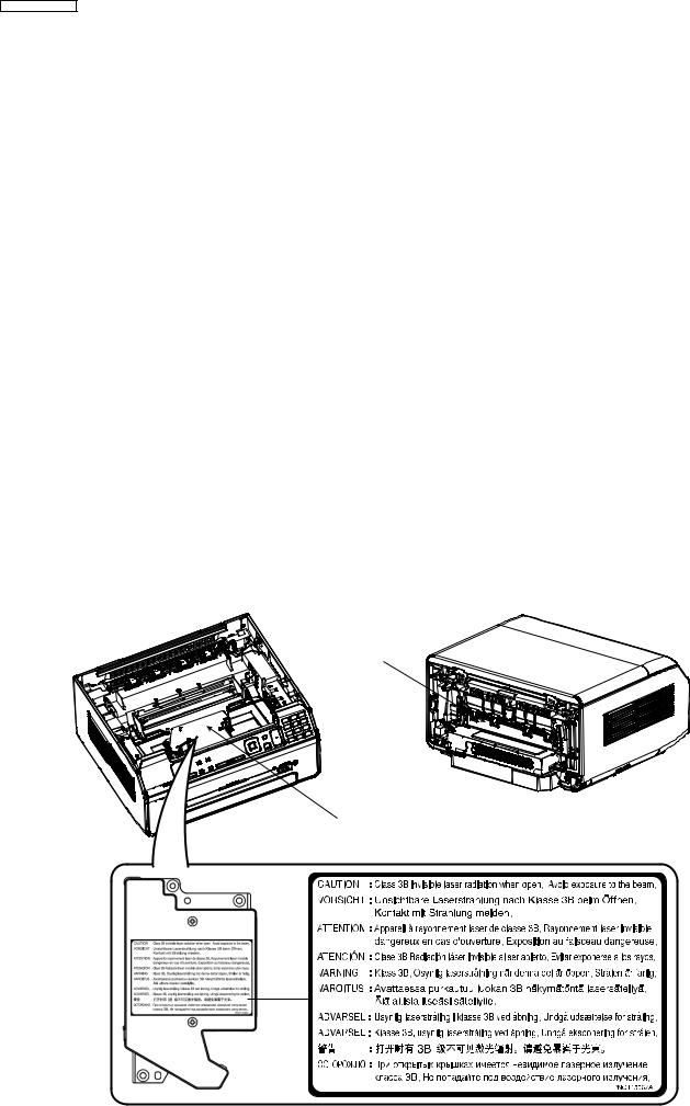
2.5.Laser Beam and Fuser Unit Section
•The printer of this unit utilizes a laser. Use of controls or adjustments or performance of procedures other than those specified herein may result in hazardous radiation exposure.
•The fuser unit is inside of the unit and gets hot. Do not touch it when removing the jammed paper or cleaning the lower glass.
Fuser Unit
Laser Scanning Unit
* In case of this figure, this Laser Caution Label is located on the other side of the LSU.
Laser
Caution
Label
8

KX-MB1500UCB
2.6.Note for Repairing
Caution
Please inform users of the danger of data being lost at the time of repair.
Data will be lost in the following situations.
1.When replacing the ROM ass'y.
2.When replacing the Main board ass'y.
3.When executing service mode #550 or #710. (Memory Clear) There is a possibility of data loss in the following situations.
1.When removing a board.
2.When writing new software to ROM.
9

KX-MB1500UCB
3 Specifications
Document Size: |
Max. 216 mm in width, Max. 297 mm in length |
Effective Scanning Width: |
208 mm |
Effective Printing Width: |
Letter/ Legal: 208 mm |
Scanning Density: |
A4: 202 mm |
Scanning resolution: |
|
|
Up to 600 × 1,200 dpi (Optical) |
|
Up to 19,200 x 19,200 dpi (Interpolated) |
|
Copy resolution: |
Photo resolution: |
Up to 600 × 600 dpi |
64-level |
|
Scanner Type: |
Colour Contact Image Sensor |
Printer Type: |
Laser printer |
Operating Environment: |
10°C-32.5°C, 20%-70% RH (Relative Humidity) |
Dimensions: |
Approx. width 380 mm x depth 360 mm x height 203 mm |
Mass (Weight): |
Approx. 9 kg |
Power Consumption: |
Standby: Approx. 4 W |
|
Preheat: Approx. 55 W |
|
Copy: Approx. 350 W |
Maximum: Approx. 950 W (When the fuser lamp turns on) Power Supply: 220-240 V AC, 50/60 Hz
Memory Capacity (for operation and 32 MB
storing memory): |
Laser output: Max. 10 mW |
Laser diode properties: |
|
|
Wavelength: 760 nm-800 nm |
Print Speed: |
Emission duration: Continuous |
A4: Approx. 18 ppm (pages per minute) |
|
Printing Resolution: |
Letter: Approx. 19 ppm (pages per minute) |
600 x 600 dpi |
|
Maximum Monthly Duty Cycle: |
5,000 printed pages |
CIS’s LED light properties: |
LED radiation output: Max. 1 mW |
|
Wavelength: |
|
Red 630 nm typical |
|
Green 520 nm typical |
|
Blue 465 nm typical |
Product life: |
Emission duration: Continuous |
30,000(Thirty thousand) pages or 5 years whichever comes first. |
Note:
•Design and specifications are subject to change without notice.
•The pictures and illustrations in these instructions may vary slightly from the actual product.
10
KX-MB1500UCB
4 General/Introduction
4.1.Optional Accessories
Model No. |
Description |
Specifications |
KX-FAT400A7 |
Replacement toner cartridge*1 |
1 toner cartridge |
KX-FAT410A7 |
Replacement toner cartridge (high capacity)*2 |
1 toner cartridge |
*1 Prints about 1,800 pages at ISO/IEC 19752 standard page.
*2 Prints about 2,500 pages at ISO/IEC 19752 standard page.
Note:
•ISO/IEC 19752 standard is as follows:
-Environment: 23 ± 2°C / 50 ± 10% RH
-Print mode: Continuous printing
4.2.Translation Lists
4.2.1.Error Message (Display)
11

KX-MB1500UCB
5 Features
5.1.General Features
General
LCD (Liquid Crystal Display) readout
Flat-Bed Multifunction Printer
Resolution: Standard/Fine/Super fine/Photo (64 level). STANDARD: For printed or typewritten originals with normalsized characters.
FINE: For originals with small printing.
SUPER FINE: For originals with very small printing. PHOTO: For originals containing photographs, shaded drawing, etc.
150-sheet paper capacity (64 g/m2 ~ 75 g/m2)
Approx. 150 pages of memory transmission Approx. 110 pages of memory reception
Enhanced Copier Function
Multi-copy function (up to 99 copies) Enlargement and reduction
64-Level halftone
5.2.Hardware Requirements for Multi-Function Software
To use Multi-Function Station on your computer, the following are required:
Operating System:
Windows 2000 / Windows XP / Windows Vista / Windows 7
CPU:
Windows 2000: Pentium®  or higher processor Windows XP: Pentium
  or higher processor
Windows Vista / Windows 7: Pentium 4 or higher processor
RAM:
Windows 2000/Windows XP: 128 MB (256 MB or more recommended) Windows Vista: 512 MB (1 GB or more recommended)
Windows 7: 1 GB (2 GB or more recommended)
Other Hardware:
CD-ROM drive
Hard disk drive with at least 600 MB of available space USB interface
Other:
Internet Explorer® 5.0 or later
Warning:
•To assure continued emission limit compliance;
-use only shielded USB cable (Example: Hi-Speed USB 2.0 certified cable).
•To protect the unit, use only shielded USB cable in areas where thunderstorms occur.
12
KX-MB1500UCB
6 Technical Descriptions
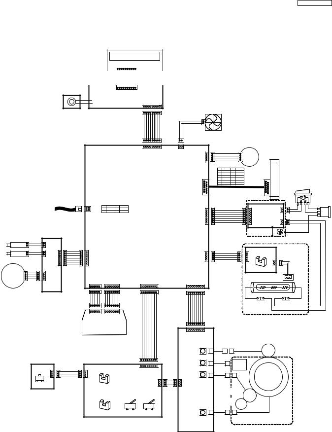
6.1.Connection Diagram
LCD
MIC
TO
PC/USB
|
CN54 |
|
REGISTER |
REG |
|
DG |
||
CLUTCH |
||
|
|
|
CN53 |
CN52 |
|
PICKUP |
PICK |
|
|
SNPICK |
|
1 |
SNREG |
||
DG |
|
|||
SOLENOID |
|
2 |
DG |
|
|
|
|||
|
|
|
3 |
2B |
|
|
|
4 |
2A |
|
|
|
5 |
1A |
|
|
|
6 |
1B |
|
|
|
7 |
|
MAIN |
|
CN55 |
|
1B |
2 |
||
1A |
|||
|
|
1 |
|
MOTOR |
2A |
3 |
|
2B |
|||
4 |
TONER CN59 |
|
SENSOR |
TNR |
1 |
GND |
2 |
5V |
3 |
|
IC53 |
|
|
|
|
|
|
|
|
|
|
|
|
|
|
DB7 |
DB6 |
DB5 |
DB4 |
E |
R / W |
RS |
V0 |
VDD |
VSS |
|
|
|
|
|
|
|
|
|
|
|
|
|
|
|
|
|
|
|
|
|
|
|
|
|
CN1
10 |
9 8 7 6 5 4 3 2 1 |
|
|
OPERATION PANEL BOARD |
|
|
|
|
|
|
|
|
|
|
|
|
|||||
|
|
|
|
|
|
|
1 2 3 4 5 6 7 8 9 |
|
|
|
|
|
|
|
|
|
|
|
|
|
|
|
|
|
|
CN2 |
|
|
|
|
|
|
|
|
|
|
|
|
|
|
|
|
|
|
|
|
|
|
|
|
|
DC FAN |
|
|
|
|
|
|
|
|
|
|
|
|
|
|
THRM KSTART KTXD KSCLK OPERST DG |
5V MIC+ MIC- |
DG FANON |
|
|
|
|
|
|
|
|
|
|
|
|
|
|
|
|
|
1 2 3 4 5 6 7 8 9 |
1 2 |
|
CN509 |
|
|
|
|
|
|
|
|
|
|
|
|
|
|
|
|
CN511 |
CN506 |
|
|
A |
|
|
|
|
|
|
|
|
|
|
|
|
|
|
|
|
|
|
|
1 |
XA |
|
|
FB |
|
|
|
|
|
|
|
|
|
|
|
|
|
|
|
2 |
XB |
|
|
|
|
|
|
|
|
|
|
|
|
|
|
|
|
|
|
3 |
B |
|
|
MOTOR |
|
|
|
|
|
|
|
|
|
|
|
|
|
|
|
4 |
|
|
|
|
|
CISMODULE |
|
|
|
|
|
|
|
|
|
|
|
|
|
|
No |
NAME |
No |
NAME |
|
|
|
|
|
|
|
|
|
|
|
|
|
|
|
|
12 |
SIG |
11 |
DG |
|
|
|
|
|
|
|
|
|
|
|
|
|
|
|
|
10 |
3.3V |
9 |
VREF |
|
|
|
|
|
|
|
|
|
|
|
|
|
|
|
CN510 |
8 |
CNT |
7 |
SI |
|
|
|
|
|
|
|
|
|
|
|
|
|
|
|
6 |
DG |
5 |
CLK |
|
|
|
|
|
|
|
|
|
|
|
|
|
|
|
|
|
|
|
|
|
||||
|
|
|
|
|
|
|
|
|
|
|
|
4 |
VLED |
3 |
LED_G |
|
|
|
|
|
|
|
|
|
|
|
|
|
|
|
|
2 |
LED_R |
1 |
LED_B |
|
|
|
|
|
|
|
|
|
|
|
|
|
|
|
|
|
|
|
|
|
|
|
POWER SW |
CN300 |
|
|
CN300 |
|
|
|
|
|
|
|
|
|
|
|
|
|
|
AC INLET |
|
1 |
4 2 |
|
No |
NAME |
No |
NAME |
|
|
|
|
CN504 |
|
|
|
CN101 |
|
CN1 |
||
|
|
|
|
|
|
|
|
|
|
LIVE |
|||||||||
|
3 |
|
1 |
VBUS |
2 |
D |
|
|
|
|
1 |
|
|
|
|
1 |
|
1 |
NEUTRAL |
|
|
|
3 |
D+ |
4 |
GND |
|
|
|
|
HTRCTL |
|
|
|
|
2 |
|||
|
|
|
|
|
|
|
|
|
|
|
2 |
5V |
|
|
|
2 |
SMPS |
|
|
|
|
|
|
|
|
|
|
|
|
|
4 |
|
|
|
|
4 |
|
|
|
|
|
|
|
|
|
|
|
|
|
|
3 |
GND |
|
|
|
3 |
|
|
|
|
|
|
|
|
|
|
|
|
|
|
5 |
GND |
|
|
|
5 |
|
CN2 |
|
|
|
|
|
|
|
|
|
|
|
|
24V |
|
|
|
|
|
HEAT LAMP |
||
|
|
|
|
|
|
|
|
|
|
|
6 |
|
|
|
6 |
|
1 |
||
|
|
|
|
|
|
MAIN BOARD |
|
|
24V |
|
|
|
|
|
|||||
|
|
|
|
|
|
|
|
7 |
|
|
|
7 |
|
|
|||||
|
|
|
|
|
|
|
|
|
|
|
|
|
2 |
|
|||||
|
|
|
|
|
|
|
|
|
|
|
|
|
|
|
|
|
|||
|
|
|
|
|
|
|
|
|
|
|
|
|
|
|
|
|
|
|
PE |
|
|
|
|
|
|
|
|
|
|
|
|
|
|
|
PSU COVER |
|
|
|
|
CN502 |
|
|
|
|
|
|
|
|
|
|
CN503 |
|
|
|
CN57 |
|
|
|
FUSER |
1 |
|
|
|
|
|
|
|
|
|
|
2 |
THRM1 |
|
|
2 |
|
|
|
UNIT |
3 |
|
|
|
|
|
|
|
|
|
|
POUT |
|
|
|
|
|
|||
2 |
|
|
|
|
|
|
|
|
|
|
1 |
3.3V |
|
|
1 |
EXIT SENSOR |
|
|
|
|
|
|
|
|
|
|
|
|
|
|
|
|
|
|
|
||||
4 |
|
|
|
|
|
|
|
|
|
|
3 |
GND |
|
|
3 |
|
CN58 |
|
|
|
|
|
|
|
|
|
|
|
|
4 |
|
|
4 |
|
|
|
|||
5 |
|
|
|
|
|
|
|
|
|
|
|
|
|
|
THRM1 |
||||
6 |
|
|
|
|
|
|
|
|
|
|
|
|
|
|
|
|
1 |
|
|
7 |
|
|
|
|
|
|
|
|
|
|
|
|
|
|
|
|
2 |
|
DG |
|
|
|
|
|
|
|
|
|
|
|
|
|
|
|
|
|
|
|
|
|
|
|
|
|
|
|
|
|
|
|
|
|
|
|
|
|
IC52 |
|
|
|
|
|
|
|
|
|
|
|
|
|
|
|
|
|
|
|
THERMISTOR |
||
CN501 |
|
CN500 |
|
|
CN508 |
|
|
CN505 |
|
|
|
|
|
|
|
|
|
||
1 2 3 4 5 |
1 2 3 4 5 6 7 |
|
1 2 3 4 5 6 7 8 |
|
|
|
|
|
|
|
|
|
|
||||||
|
|
1 2 3 4 5 6 7 8 |
|
|
|
|
|
|
|
|
|||||||||
|
|
|
|
|
|
|
|
|
|
|
|
|
|
|
|
|
|
||
POLCLK XREADY |
POLON DG |
|
|
DG XHSYNC XVIDEO XLDEN XAPC |
|
|
5V REG PTOP GND BATTERY |
|
|
|
|
|
|
|
|
|
HEAT LAMP |
||
24V |
5VLD |
DG |
5VLD |
TNR |
F-USE |
TRS DEV CHG GND HVFUSE |
24V |
|
|
|
|
THERMOSTAT |
|
THERMOSTAT |
|||||
|
|
|
LSU |
|
|
|
|
|
|
|
|
|
|
|
|
|
|
|
|
|
|
|
|
|
|
|
|
|
CN1 |
1 2 3 4 5 6 7 8 |
|
|
|
|
|
|
|
|
|
|
|
|
|
|
|
|
|
|
|
|
|
|
|
|
|
|
TRANSCRIPTION |
||
|
|
|
|
|
|
|
|
|
|
|
|
|
|
|
|
|
|
ROLLER |
|
|
|
|
|
|
|
|
|
|
|
TRA |
|
|
|
|
|
|
|
|
|
|
|
|
|
|
|
|
|
|
|
DRUM |
|
|
|
|
|
|
|
|
|
|
|
|
|
|
|
|
|
|
|
LIFE |
|
|
|
|
|
|
|
|
|
CN56 |
|
REGISTERS |
|
CN50 |
|
|
|
|
|
|
|
|
|
|
|
|
|
||
|
|
|
1 2 3 4 5 6 7 8 |
|
|
|
|
|
|
|
|
|
|
|
|||||
1 |
|
|
ENSOR |
|
|
|
|
|
|
|
|
|
|
|
|
|
|
|
|
|
|
|
|
|
|
|
|
|
DEV |
|
|
|
|
|
|
|
|
|
|
2 |
|
|
|
|
|
|
|
|
|
|
|
|
|
|
|
|
|
|
|
3 |
|
|
|
|
|
|
|
CN51 |
CN2 |
|
|
|
|
|
|
|
|
|
|
|
|
|
|
|
|
|
|
|
|
|
|
|
|
|
|
|
|
||
|
|
|
|
|
|
|
|
1 |
24VIL |
|
|
|
|
|
|
|
|
|
|
|
|
|
|
|
|
|
|
|
|
|
|
|
|
|
|
|
|
|
|
|
|
|
|
|
|
|
|
2 |
24V |
|
|
|
|
|
|
|
|
|
|
|
|
|
IC51 |
|
|
|
3 |
|
|
|
|
|
|
|
|
|
|
||
|
|
|
|
|
|
|
|
|
|
|
|
|
|
|
|
|
|||
|
|
|
|
|
|
|
|
|
|
|
|
|
DEVELOPING |
|
|
|
|
||
|
|
|
PTOP |
|
5V Interlock |
24V Interlock |
|
|
HVPS |
|
|
ROLLER |
|
|
|
OPC |
|||
|
|
|
SENSOR |
|
Switch |
Switch |
|
|
|
|
TONER SUPPLY |
|
|
|
|
DRUM |
|||
|
|
|
|
|
|
|
|
|
|
|
|
|
|
|
|
||||
|
|
|
|
|
|
|
|
|
|
|
|
ROLLER |
|
|
|
|
|
|
|
|
|
|
IC50 |
|
SW50 |
SW51 |
|
|
CHG |
|
|
|
|
|
|
|
|
|
|
|
|
|
|
|
|
|
|
|
|
|
|
|
|
|
|
|
|||
DRUM UNIT
13

KX-MB1500UCB
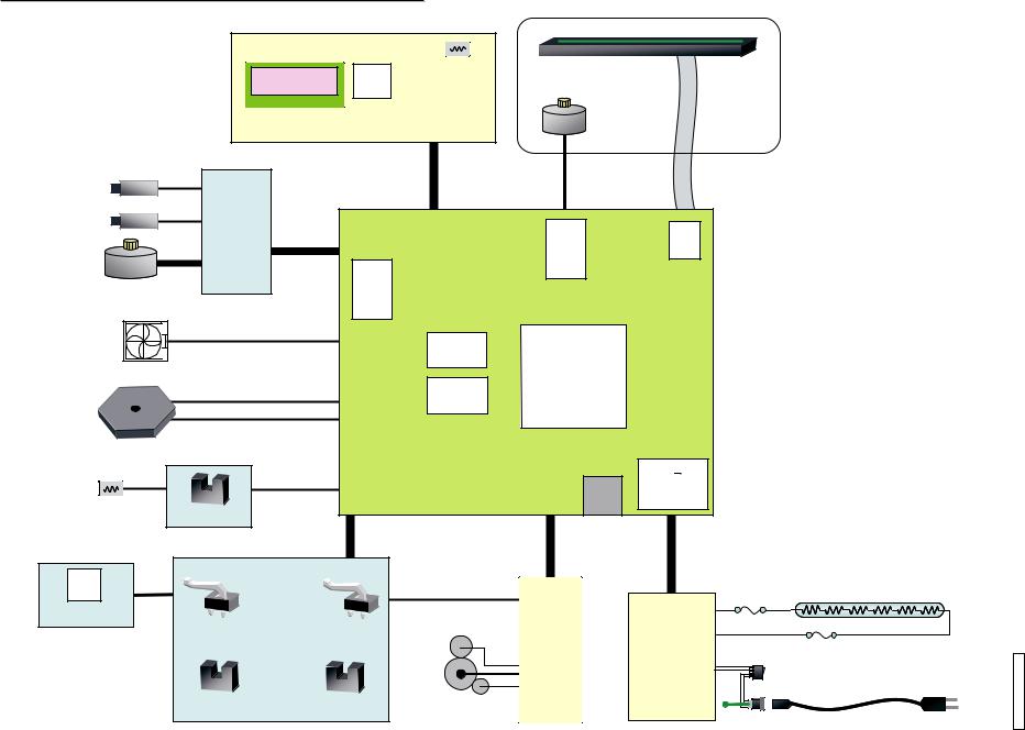
6.2.General Block Diagram
MAIN UNIT
SOC (IC300)
This custom IC is used for general MFP operations.
1) |
CPU |
ARM9 operating at 250MHz. |
2) |
SDRAM Controller |
Controls SDRAM Memory. |
3) |
USB Controller with PHY |
Apply to USB2.0 HS |
4) |
Scanner I/F |
Controls the CIS and AFE, and process the scan images. |
5) |
LSU I/F |
Controls the polygon motor and outputs the VIDEO signal to LSU. |
6) |
MOTOR I/F |
Controls the DC motor and Stepping Motor. |
7) |
FAN I/F |
Controls FAN MOTOR and detect the rotation of FAN MOTOR. |
8) |
OPERATION PANEL I/F |
Serial interface with Operation Panel. |
9) |
SENSOR I/F |
Detects the sensor signal. |
10) |
I/O PORT |
I/O Port Interface. |
11) |
A/D, D/A converter |
Sends beep tones, etc. |
|
|
Convert the analog signal to the digital signal. |
ROM (IC402)
This 8MB FLASH ROM contains all of the program instructions on the unit operations.
SYNCHRONOUS DYNAMIC RAM (IC400)
This 256Mbit SDRAM is used for CPU work and receiving memory and page memory.
POWER SUPPLY
DC-DC converters generate 3.3V and 1.2V for system power.
Regurator generates 5V for peripheral devices.
READ SECTION
CIS Unit to read transmitted documents.
Scan data is converted by AFE(IC503).
MOTOR
This model has 2 stepping motors.
IC600 drives the stepping motor for printing.
IC502 drives the stepping motor for CIS carriage.
LSU
Forms the images on the OPC DRUM by rotating polygon motor and reflecting the laser beam against polygon.
SENSORS
Composed of 2 switches and 3 sensors.
POWER SUPPLY BOARD
Supplies +24V and +5V to the Main unit and controls the Heat Lamp.
HIGH VOLTAGE POWER SUPPLY BOARD
Supplies bias need for the printing operation: bias of the DRUM, Developing and Transcription.
FIXING UNIT
Composed heat lamp, thermistor and thermostats.
14
15
MB1520 series System Schematic
|
|
|
Flat Bed |
|
Operation Panel Board |
|
|
||
2Line |
Ope |
Thermistor |
Color CIS |
|
(Room) |
|
|||
LCD |
G/A |
Carriage motor |
||
|
||||
Regist Clutch |
AMP2 |
JST4 |
FFC 12 |
AMP9 |
Pick Up Solenoid |
JST2 |
|
Main Board |
|
|
|
|
|
|
|
Motor |
|
|
||
|
|
|
AMP7 |
|
AFE |
|
|
|
AMP4 |
|
Driver |
|
|||
Main motor |
|
|
|
|
|||
|
|
(FB) |
|
|
|||
|
|
|
Motor |
|
|
||
|
|
|
|
|
|
|
|
|
|
|
|
Driver |
|
|
|
|
|
|
|
(Main) |
|
|
|
FAN |
|
|
JST2 |
FLASH |
|
|
|
|
|
|
|
|
|
||
|
|
|
|
|
|
|
|
|
|
|
|
(64Mbit) |
Sirius |
|
|
|
|
|
|
|
|
|
|
|
|
|
AMP7(Blue) |
SDRAM |
Lite |
|
|
LSU |
|
|
|
(256Mbit ) |
|
|
|
|
|
|
|
|
|
|
|
|
|
|
AMP5 |
|
|
|
|
|
JST2 |
|
AMP4 |
|
|
5V |
|
|
|
|
USB |
3.3V/1.2V |
|
||
Thermistor |
|
|
|
DC-DC |
|
||
|
|
|
|
|
|
||
(Heater) |
|
EXIT Sensor |
|
|
|
|
|
|
|
|
|
AMP8 |
AMP8(Blue) |
AMP7 |
|
Hall |
AMP3 |
5V Interlock |
24V Interlock |
|
|
|
|
|
|
|
|
|
|
||
|
|
|
AMP3(Blue) |
HVPS |
|
|
|
IC |
|
|
|
Thermostat |
Heater |
||
|
|
|
|
|
|
||
Toner Sensor |
|
|
|
|
|
SMPS |
|
|
|
|
|
|
|
|
|
|
|
Thermostat |
|
Power SW |
|
Regist Sensor |
PTOP Sensor |
AC |
|
||
|
AC inlet |
AC cord set |
MB1500UCB-KX
KX-MB1500UCB
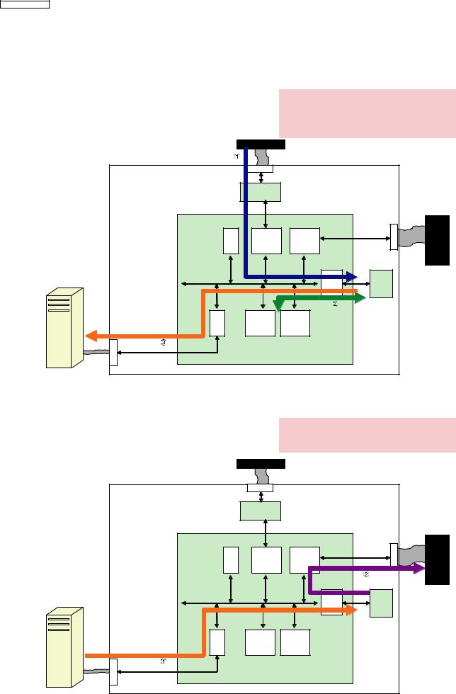
6.3.Main Board Section
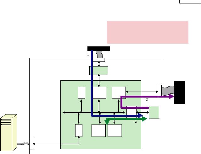
6.3.1.Data Flow
[PC Scan]
CIS unit
1. An analog image data is output from CIS unit to IC503.
IC503 decode the analog data to digital data, and output to IC300. Scanner I/F in IC300 process image data and store it in IC400 through SDRAM I/F.
2.If necessary, the data is compressed via DSP.
3.The data is output to PC through the USB I/F.
Main Board |
|
|
CN510 |
|
|
|
|
|
|
|
|
|
|
|
AFE |
IC503 |
|
|
|
|
|
IC300 |
LSU |
|
|
CPU |
Scanner |
Print I/F |
CN500 |
|
|
I/F |
|||
|
|
|
|
|
|
|
|
|
|
|
IC400 |
PC |
|
|
|
SDRAM |
SDRAM |
|
|
|
I/F |
||
|
|
|
|
||
|
|
|
|
|
|
|
USB |
|
JBIG |
DSP |
|
|
I/F |
|
|
||
|
|
|
|
|
|
CN300 |
|
|
|
|
|
USB |
|
|
|
|
|
[PC print] |
|
|
|
|
|
1. The print data is output from PC through USB and pass the USB I/F in IC300.
then the data is stored in IC400 through SDRAM I/F.
2. Print I/F retrieve the data from IC400 and output it to LSU.
CIS unit
Main Board |
|
|
CN510 |
|
|
|
|
|
|
|
|
|
|
|
AFE |
IC503 |
|
|
|
|
|
IC300 |
LSU |
|
|
CPU |
Scanner |
Print I/F |
CN500 |
|
|
I/F |
|||
|
|
|
|
|
|
|
|
|
|
|
IC400 |
PC |
|
|
|
SDRAM |
SDRAM |
|
|
|
I/F |
||
|
|
|
|
||
|
|
|
|
|
|
|
USB |
|
JBIG |
DSP |
|
|
I/F |
|
|
||
|
|
|
|
|
|
CN300 |
|
|
|
|
|
USB |
|
|
|
|
|
|
|
|
16 |
|
|
KX-MB1500UCB
[Copy]
1. An analog image data is output from CIS unit to IC503.
IC503 decode the analog data to digital data, and output to IC300. Scanner I/F in IC300 process image data and store it in IC400 through SDRAM I/F.
2. If necessary, the data is compressed via JBIG.
3. Print I/F retrieve the data from IC400 and output it to LSU.
CIS unit
Main Board |
|
CN510 |
|
|
|
|
|
|
|
|
|
AFE |
IC503 |
|
|
|
|
IC300 |
LSU |
|
CPU |
Scanner |
Print I/F |
CN500 |
|
I/F |
|||
|
|
|
|
|
|
|
|
|
IC400 |
PC |
|
|
SDRAM |
SDRAM |
|
|
I/F |
||
|
|
|
||
|
|
|
|
|
|
USB |
JBIG |
DSP |
|
|
I/F |
|
||
|
|
|
|
|
CN300 |
|
|
|
|
USB |
|
|
|
|
17

KX-MB1500UCB
Description of Pin Distribution (IC300) SOC (System On Chip)
PIN NO. |
PinName |
I/O |
POWER SUPPLY VOLTAGE |
EXPLANATION |
A02 |
LEDONB |
O |
3.3V |
SCANNER INTERFACE |
A03 |
NCCDON |
O |
3.3V |
SCANNER INTERFACE |
A04 |
AFEMCLK |
O |
3.3V |
SCANNER INTERFACE |
A05 |
NCCDCP |
O |
3.3V |
NOT USED |
A06 |
CCDCLK |
O |
3.3V |
NOT USED |
A07 |
PIO29 |
O |
3.3V |
OPERATION PANEL INTERFACE |
A08 |
PIO57 |
O |
3.3V |
CARRIAGE MOTOR INTERFACE |
A09 |
PIO53 |
O |
3.3V |
CARRIAGE MOTOR INTERFACE |
A10 |
PIO50 |
O |
3.3V |
CARRIAGE MOTOR INTERFACE |
A11 |
PIO46 |
O |
3.3V |
FAN1 CONTROL |
A12 |
PIO42 |
O |
3.3V |
DC MOTOR INTERFACE |
A13 |
NFRCE |
O |
3.3V |
FLASH MEMORY CHIP SELECT |
A14 |
FRMD0 |
I/O |
3.3V |
FLASH MEMORY DATA BUS 0 |
A15 |
FRMD3 |
I/O |
3.3V |
FLASH MEMORY DATA BUS 3 |
A16 |
FRMD7 |
I/O |
3.3V |
FLASH MEMORY DATA BUS 7 |
A17 |
FRMA3 |
O |
3.3V |
FLASH MEMORY ADDRESS BUS 3 |
A18 |
FRMA6 |
O |
3.3V |
FLASH MEMORY ADDRESS BUS 6 |
A19 |
FRMA10 |
O |
3.3V |
FLASH MEMORY ADDRESS BUS 10 |
A20 |
THRMAVDD |
- |
3.3V |
POWER SUPPLY |
A21 |
FRMA11 |
O |
3.3V |
FLASH MEMORY ADDRESS BUS 11 |
A22 |
FRMA15 |
O |
3.3V |
FLASH MEMORY ADDRESS BUS 15 |
A23 |
FRMA17 |
O |
3.3V |
FLASH MEMORY ADDRESS BUS 17 |
A24 |
FRMA20 |
O |
3.3V |
FLASH MEMORY ADDRESS BUS 20 |
A25 |
FRMA22 |
O |
3.3V |
FLASH MEMORY ADDRESS BUS 22 |
AA01 |
SDMD8 |
I/O |
3.3V |
SDRAM DATA BUS 8 |
AA02 |
SDMD9 |
I/O |
3.3V |
SDRAM DATA BUS 9 |
AA03 |
SDMA7 |
O |
3.3V |
SDRAM ADDRESS BUS 7 |
AA04 |
SDMA6 |
O |
3.3V |
SDRAM ADDRESS BUS 6 |
AA23 |
VDD1.2 |
- |
1.2V |
POWER SUPPLY |
AA24 |
AFERST |
O |
3.3V |
NCU INTERFACE |
AA25 |
RING |
I |
3.3V |
NCU INTERFACE |
AA26 |
EXTINT |
I |
3.3V |
NCU INTERFACE |
AB01 |
SDMD10 |
I/O |
3.3V |
SDRAM DATA BUS 10 |
AB02 |
SDMD11 |
I/O |
3.3V |
SDRAM DATA BUS 11 |
AB03 |
SDMA5 |
O |
3.3V |
SDRAM ADDRESS BUS 5 |
AB04 |
VDD1.2 |
- |
1.2V |
POWER SUPPLY |
AB23 |
VSS |
- |
GND |
GND |
AB24 |
BTXD |
O |
3.3V |
NCU INTERFACE |
AB25 |
BRXD |
I |
3.3V |
NCU INTERFACE |
AB26 |
AFECLK |
O |
3.3V |
NCU INTERFACE |
AC01 |
SDMD12 |
I/O |
3.3V |
SDRAM DATA BUS 12 |
AC02 |
SDMD13 |
I/O |
3.3V |
SDRAM DATA BUS 13 |
AC03 |
SDMA4 |
O |
3.3V |
SDRAM ADDRESS BUS 4 |
AC04 |
VSS |
- |
GND |
GND |
AC05 |
VSS |
- |
GND |
GND |
AC06 |
VDD1.2 |
- |
1.2V |
POWER SUPPLY |
AC07 |
TXD0 |
O |
3.3V |
ETHERNET INTERFACE |
AC08 |
TX_ER |
O |
3.3V |
ETHERNET INTERFACE |
AC09 |
RXD1 |
I |
3.3V |
ETHERNET INTERFACE |
AC10 |
VDD3.3 |
- |
3.3V |
POWER SUPPLY |
AC11 |
TEST |
I |
3.3V |
NOT USED |
AC12 |
USBREXT |
I |
3.3V |
USB INTERFACE |
AC13 |
VDD1.2 |
- |
1.2V |
POWER SUPPLY |
AC14 |
VDD3.3 |
- |
3.3V |
POWER SUPPLY |
AC15 |
USBXIN |
I |
3.3V |
CRYSTAL(12MHz) INPUT |
AC16 |
LSI_SCAN_ENABLE |
I |
3.3V |
NOT USED |
AC17 |
VDD1.2 |
- |
1.2V |
POWER SUPPLY |
AC18 |
NWDTRST |
O |
3.3V |
WATCH DOG TIMER RESET OUTPUT |
AC19 |
LSI_TN |
I |
3.3V |
NOT USED |
AC20 |
PSCIO2 |
I |
3.3V |
INPUT PORT (FANDET1) |
AC21 |
PSCIO6 |
O |
3.3V |
NOT USED |
AC22 |
VDD1.2 |
- |
1.2V |
POWER SUPPLY |
AC23 |
VSS |
- |
GND |
GND |
AC24 |
ATXD |
O |
3.3V |
NCU INTERFACE |
AC25 |
BBITCLK |
I/O |
3.3V |
NCU INTERFACE |
18

KX-MB1500UCB
PIN NO. |
PinName |
I/O |
POWER SUPPLY VOLTAGE |
EXPLANATION |
AC26 |
BSPCLK |
I/O |
3.3V |
NCU INTERFACE |
AD01 |
SDMD14 |
I/O |
3.3V |
SDRAM DATA BUS 14 |
AD02 |
SDMD15 |
I/O |
3.3V |
SDRAM DATA BUS 15 |
AD03 |
VSS |
- |
GND |
GND |
AD04 |
NBATRST |
I |
3.3V |
BATTERY RESET INPUT |
AD05 |
VDD2RTC |
- |
1.2V |
POWER SUPPLY |
AD06 |
CRS |
I |
3.3V |
ETHERNET INTERFACE |
AD07 |
TXD1 |
O |
3.3V |
ETHERNET INTERFACE |
AD08 |
RX_DV |
I |
3.3V |
ETHERNET INTERFACE |
AD09 |
RXD2 |
I |
3.3V |
ETHERNET INTERFACE |
AD10 |
RX_ER |
I |
3.3V |
ETHERNET INTERFACE |
AD11 |
CLKSEL |
I |
3.3V |
NOT USED |
AD12 |
USBVSSA33_BIAS |
- |
GND |
GND |
AD13 |
USBVSSA33 |
- |
GND |
GND |
AD14 |
USBVDDA12_SQ |
- |
1.2V |
POWER SUPPLY |
AD15 |
USBVSSA12 |
- |
GND |
GND |
AD16 |
LSI_TRSTN |
I |
3.3V |
NOT USED |
AD17 |
LSI_TDO |
O |
3.3V |
NOT USED |
AD18 |
NRST |
I |
3.3V |
SYSTEM RESET INPUT |
AD19 |
HTRCTL |
O |
3.3V |
HEATER CONTROL |
AD20 |
PSCIO3 |
I |
3.3V |
INPUT PORT (POUT) |
AD21 |
PSCIO7 |
O |
3.3V |
NOT USED |
AD22 |
PSCIO15 |
I |
3.3V |
INPUT PORT (RPS) |
AD23 |
NC |
- |
- |
NOT USED |
AD24 |
VSS |
- |
GND |
GND |
AD25 |
ASPCLK |
I/O |
3.3V |
NCU INTERFACE |
AD26 |
ARXD |
I |
3.3V |
NCU INTERFACE |
AE01 |
SDLDM1 |
O |
3.3V |
SDRAM DQML1 |
AE02 |
VSS |
- |
GND |
GND |
AE03 |
SYSPLLVSS1 |
- |
GND |
GND |
AE04 |
RTCCLKOUT |
O |
3.3V |
CRYSTAL(32.768KHz) OUTPUT |
AE05 |
RTCPWRDWN |
I |
3.3V |
RTC POWER DOWN |
AE06 |
TX_CLKI |
I |
3.3V |
ETHERNET INTERFACE |
AE07 |
TXD2 |
O |
3.3V |
ETHERNET INTERFACE |
AE08 |
RX_CLKI |
I |
3.3V |
ETHERNET INTERFACE |
AE09 |
RXD3 |
I |
3.3V |
ETHERNET INTERFACE |
AE10 |
MDC |
O |
3.3V |
ETHERNET INTERFACE |
AE11 |
NC |
- |
- |
NOT USED |
AE12 |
USBID |
O |
3.3V |
NOT USED |
AE13 |
USBDM |
I/O |
3.3V |
USB INTERFACE |
AE14 |
USBVSSA12_SQ |
- |
GND |
GND |
AE15 |
USBVDDA12PLL |
- |
1.2V |
POWER SUPPLY |
AE16 |
USBVDDA12 |
- |
1.2V |
POWER SUPPLY |
AE17 |
LSI_TDI |
I |
3.3V |
NOT USED |
AE18 |
LSI_PROCMON |
O |
3.3V |
NOT USED |
AE19 |
LSI_IDDT |
I |
3.3V |
NOT USED |
AE20 |
PSCIO1 |
I |
3.3V |
INPUT PORT (PICK) |
AE21 |
PSCIO5 |
O |
3.3V |
NOT USED |
AE22 |
PSCIO13 |
I |
3.3V |
INPUT PORT (TNR) |
AE23 |
MDMCLKOUT |
O |
3.3V |
CRYSTAL(24.576MHz) OUTPUT |
AE24 |
MDMPLLVDD |
- |
3.3V |
POWER SUPPLY |
AE25 |
VSS |
- |
GND |
GND |
AE26 |
ABITCLK |
I/O |
3.3V |
NCU INTERFACE |
AF02 |
SYSPLLVDD1 |
- |
3.3V |
POWER SUPPLY |
AF03 |
VDD3.3OSC |
- |
3.3V |
POWER SUPPLY |
AF04 |
RTCCLKIN |
I |
3.3V |
CRYSTAL(32.768KHz) INPUT |
AF05 |
COL |
I |
3.3V |
ETHERNET INTERFACE |
AF06 |
TX_EN |
O |
3.3V |
ETHERNET INTERFACE |
AF07 |
TXD3 |
O |
3.3V |
ETHERNET INTERFACE |
AF08 |
RXD0 |
I |
3.3V |
ETHERNET INTERFACE |
AF09 |
MDIO |
I/O |
3.3V |
ETHERNET INTERFACE |
AF10 |
MGTINT |
I |
3.3V |
ETHERNET INTERFACE |
AF11 |
USBVBUS |
O |
3.3V |
USB INTERFACE |
AF12 |
USBVDDA33_BIAS |
- |
3.3V |
POWER SUPPLY |
AF13 |
USBDP |
I/O |
3.3V |
USB INTERFACE |
AF14 |
USBVDDA33 |
- |
3.3V |
POWER SUPPLY |
AF15 |
USBVSSA12PLL |
- |
GND |
GND |
19

KX-MB1500UCB
PIN NO. |
PinName |
I/O |
POWER SUPPLY VOLTAGE |
EXPLANATION |
AF16 |
USBXOUT |
I |
3.3V |
CRYSTAL(12MHz) OUTPUT |
AF17 |
LSI_TMS |
I |
3.3V |
NOT USED |
AF18 |
LSI_TCK |
I |
3.3V |
NOT USED |
AF19 |
LSI_CW_TAP |
I |
3.3V |
NOT USED |
AF20 |
PSCIO0 |
I |
3.3V |
INPUT PORT (REGIST) |
AF21 |
PSCIO4 |
O |
3.3V |
NOT USED |
AF22 |
PSCIO12 |
I |
3.3V |
INPUT PORT (POUT) |
AF23 |
PSCIO14 |
I |
3.3V |
INPUT PORT (DOCU) |
AF24 |
MDMCLKIN |
I |
3.3V |
CRYSTAL(24.576MHz) INPUT |
AF25 |
MDMPLLVSS |
- |
GND |
GND |
B01 |
AFEADC0 |
I |
3.3V |
NOT USED |
B02 |
VSS |
- |
GND |
GND |
B03 |
LEDONG |
O |
3.3V |
SCANNER INTERFACE |
B04 |
AFERSMP |
O |
3.3V |
NOT USED |
B05 |
AFEVSMP |
O |
3.3V |
SCANNER INTERFACE |
B06 |
NCCDRS |
O |
3.3V |
SCANNER INTERFACE |
B07 |
PIO30 |
I/O |
3.3V |
OPERATION PANEL INTERFACE |
B08 |
MMPWR |
O |
3.3V |
NOT USED |
B09 |
PIO54 |
O |
3.3V |
CARRIAGE MOTOR INTERFACE |
B10 |
PIO51 |
O |
3.3V |
CARRIAGE MOTOR INTERFACE |
B11 |
PIO47 |
O |
3.3V |
NOT USED |
B12 |
PIO43 |
O |
3.3V |
DC MOTOR INTERFACE |
B13 |
NFROE |
O |
3.3V |
FLASH MEMORY CHIP OUTPUT ENABLE |
B14 |
FRMD1 |
I/O |
3.3V |
FLASH MEMORY DATA BUS 1 |
B15 |
FRMD4 |
I/O |
3.3V |
FLASH MEMORY DATA BUS 4 |
B16 |
FRMA0 |
O |
3.3V |
FLASH MEMORY ADDRESS BUS 0 |
B17 |
FRMA4 |
O |
3.3V |
FLASH MEMORY ADDRESS BUS 4 |
B18 |
FRMA7 |
O |
3.3V |
FLASH MEMORY ADDRESS BUS 7 |
B19 |
THRMAVSS |
- |
GND |
GND |
B20 |
TONE |
O |
3.3V |
ANALOG(TONE) OUTPUT |
B21 |
FRMA12 |
O |
3.3V |
FLASH MEMORY ADDRESS BUS 12 |
B22 |
FRMA16 |
O |
3.3V |
FLASH MEMORY ADDRESS BUS 16 |
B23 |
FRMA19 |
O |
3.3V |
FLASH MEMORY ADDRESS BUS 19 |
B24 |
FRMA21 |
O |
3.3V |
FLASH MEMORY ADDRESS BUS 21 |
B25 |
VSS |
- |
GND |
GND |
B26 |
DOTPLLVSS |
- |
GND |
GND |
C01 |
AFEADC3 |
I |
3.3V |
NOT USED |
C02 |
AFEADC1 |
I |
3.3V |
NOT USED |
C03 |
VSS |
- |
GND |
GND |
C04 |
LEDONR |
O |
3.3V |
SCANNER INTERFACE |
C05 |
OEB |
O |
3.3V |
NOT USED |
C06 |
CCDSH |
O |
3.3V |
SCANNER INTERFACE |
C07 |
PIO31 |
O |
3.3V |
OPERATION PANEL INTERFACE |
C08 |
OPMPWR |
O |
3.3V |
NOT USED |
C09 |
PIO55 |
O |
3.3V |
CARRIAGE MOTOR INTERFACE |
C10 |
PIO52 |
O |
3.3V |
CARRIAGE MOTOR INTERFACE |
C11 |
PIO49 |
O |
3.3V |
OUTPUT PORT(HSSPMUTE) |
C12 |
PIO45 |
O |
3.3V |
DC MOTOR INTERFACE |
C13 |
NFRWE |
O |
3.3V |
FLASH MEMORY CHIP WRITE ENABLE |
C14 |
FRMD2 |
I/O |
3.3V |
FLASH MEMORY DATA BUS 2 |
C15 |
FRMD6 |
I/O |
3.3V |
FLASH MEMORY DATA BUS 6 |
C16 |
FRMA2 |
O |
3.3V |
FLASH MEMORY ADDRESS BUS 2 |
C17 |
FRMA5 |
O |
3.3V |
FLASH MEMORY ADDRESS BUS 5 |
C18 |
FRMA9 |
O |
3.3V |
FLASH MEMORY ADDRESS BUS 9 |
C19 |
THRMSTR0 |
I |
3.3V |
ANALOG INPUT(THERMISTOR) |
C20 |
TONEAVDD |
- |
3.3V |
POWER SUPPLY |
C21 |
FRMA14 |
O |
3.3V |
FLASH MEMORY ADDRESS BUS 14 |
C22 |
FRMA18 |
O |
3.3V |
FLASH MEMORY ADDRESS BUS 18 |
C23 |
FRMA23 |
O |
3.3V |
FLASH MEMORY ADDRESS BUS 23 |
C24 |
VSS |
- |
GND |
GND |
C25 |
DOTPLLVDD |
- |
3.3V |
POWER SUPPLY |
C26 |
DOTCLKIN |
I |
3.3V |
CRYSTAL(20MHz) INPUT |
D01 |
AFEADC5 |
I |
3.3V |
SCANNER INTERFACE |
D02 |
AFEADC4 |
I |
3.3V |
SCANNER INTERFACE |
D03 |
AFEADC2 |
I |
3.3V |
NOT USED |
D04 |
VSS |
- |
GND |
GND |
D05 |
VSS |
- |
GND |
GND |
20
KX-MB1500UCB
PIN NO. |
PinName |
I/O |
POWER SUPPLY VOLTAGE |
EXPLANATION |
D06 |
VDD1.2 |
- |
1.2V |
POWER SUPPLY |
D07 |
PIO32 |
O |
3.3V |
OPERATION PANEL INTERFACE |
D08 |
CRMPWR |
O |
3.3V |
MOTOR CURRENT CONTROL |
D09 |
PIO56 |
O |
3.3V |
NOT USED |
D10 |
VDD1.2 |
- |
1.2V |
POWER SUPPLY |
D11 |
PIO48 |
O |
3.3V |
NOT USED |
D12 |
PIO44 |
O |
3.3V |
DC MOTOR INTERFACE |
D13 |
VDD3.3 |
- |
3.3V |
POWER SUPPLY |
D14 |
VDD1.2 |
- |
1.2V |
POWER SUPPLY |
D15 |
FRMD5 |
I/O |
3.3V |
FLASH MEMORY DATA BUS 5 |
D16 |
FRMA1 |
O |
3.3V |
FLASH MEMORY ADDRESS BUS 1 |
D17 |
VDD3.3 |
- |
3.3V |
POWER SUPPLY |
D18 |
FRMA8 |
O |
3.3V |
FLASH MEMORY ADDRESS BUS 8 |
D19 |
THRMSTR1 |
I |
3.3V |
ANALOG INPUT(THERMISTOR) |
D20 |
TONEAVSS |
- |
GND |
GND |
D21 |
FRMA13 |
O |
3.3V |
FLASH MEMORY ADDRESS BUS 13 |
D22 |
VDD1.2 |
- |
1.2V |
POWER SUPPLY |
D23 |
VSS |
- |
GND |
GND |
D24 |
NC |
- |
- |
NOT USED |
D25 |
DOTCLKOUT |
O |
3.3V |
CRYSTAL(20MHz) OUTPUT |
D26 |
PIO66 |
O |
3.3V |
NOT USED |
E01 |
SDUDM0 |
O |
3.3V |
SDRAM DQMU0 |
E02 |
AFEADC7 |
I |
3.3V |
SCANNER INTERFACE |
E03 |
AFEADC6 |
I |
3.3V |
SCANNER INTERFACE |
E04 |
VSS |
- |
GND |
GND |
E23 |
VDD1.2 |
- |
1.2V |
POWER SUPPLY |
E24 |
FRMA24 |
O |
3.3V |
FLASH MEMORY ADDRESS BUS 24 |
E25 |
PIO65 |
O |
3.3V |
NOT USED |
E26 |
PIO64 |
O |
3.3V |
NOT USED |
F01 |
SDMD16 |
I/O |
3.3V |
SDRAM DATA BUS 16 |
F02 |
SDMD17 |
I/O |
3.3V |
SDRAM DATA BUS 17 |
F03 |
AFESIFCLK |
O |
3.3V |
SCANNER INTERFACE |
F04 |
VDD1.2 |
- |
1.2V |
POWER SUPPLY |
F23 |
PIO24 |
I |
3.3V |
LSU INTERFACE |
F24 |
PIO61 |
O |
3.3V |
OUTPUT PORT(SPMUTE) |
F25 |
PIO60 |
O |
3.3V |
NOT USED |
F26 |
PIO3 |
O |
3.3V |
LSU INTERFACE |
G01 |
SDMD18 |
I/O |
3.3V |
SDRAM DATA BUS 18 |
G02 |
SDMD19 |
I/O |
3.3V |
SDRAM DATA BUS 19 |
G03 |
AFESIFDIN |
I |
3.3V |
SCANNER INTERFACE |
G04 |
AFESIFEN |
O |
3.3V |
SCANNER INTERFACE |
G23 |
PSCIO24 |
I |
3.3V |
LSU INTERFACE |
G24 |
PIO2 |
O |
3.3V |
LSU INTERFACE |
G26 |
PIO58 |
O |
3.3V |
OUTPUT PORT(CIDRLY) |
H01 |
SDMD20 |
I/O |
3.3V |
SDRAM DATA BUS 20 |
H02 |
SDMD21 |
I/O |
3.3V |
SDRAM DATA BUS 21 |
H03 |
NSDCS2 |
O |
3.3V |
SDRAM CHIP SELECT 2 |
H04 |
AFESIFDOUT |
O |
3.3V |
SCANNER INTERFACE |
H23 |
PIO63 |
O |
3.3V |
LSU INTERFACE |
H24 |
PIO62 |
O |
3.3V |
LSU INTERFACE |
H25 |
PIO28 |
O |
3.3V |
NOT USED |
H26 |
PIO21 |
O |
3.3V |
LSU INTERFACE |
J01 |
SDMD22 |
I/O |
3.3V |
SDRAM DATA BUS 22 |
J02 |
SDMD23 |
I/O |
3.3V |
SDRAM DATA BUS 23 |
J03 |
SDMA3 |
O |
3.3V |
SDRAM ADDRESS BUS 3 |
J04 |
SDMA2 |
O |
3.3V |
SDRAM ADDRESS BUS 2 |
J23 |
PIO6 |
O |
3.3V |
HIGH VOLTAGE UNIT INTERFACE |
J24 |
PIO27 |
O |
3.3V |
NOT USED |
J25 |
PIO5 |
O |
3.3V |
HIGH VOLTAGE UNIT INTERFACE |
J26 |
PIO4 |
O |
3.3V |
HIGH VOLTAGE UNIT INTERFACE |
K01 |
VSS |
- |
GND |
GND |
K02 |
SDCLK2 |
O |
3.3V |
SDRAM CLOCK 2 |
K03 |
VSS |
- |
GND |
GND |
K04 |
VDD3.3 |
- |
3.3V |
POWER SUPPLY |
K23 |
VDD1.2 |
- |
1.2V |
POWER SUPPLY |
K24 |
PIO41 |
O |
3.3V |
NOT USED |
K25 |
PIO40 |
O |
3.3V |
NOT USED |
21

KX-MB1500UCB
PIN NO. |
PinName |
I/O |
POWER SUPPLY VOLTAGE |
EXPLANATION |
K26 |
PIO39 |
O |
3.3V |
NOT USED |
L01 |
SDMD24 |
I/O |
3.3V |
SDRAM DATA BUS 24 |
L02 |
SDMD25 |
I/O |
3.3V |
SDRAM DATA BUS 25 |
L03 |
SDMA1 |
O |
3.3V |
SDRAM ADDRESS BUS 1 |
L04 |
SDMAÇO |
O |
3.3V |
SDRAM ADDRESS BUS 0 |
L11 |
VSS |
- |
GND |
GND |
L12 |
VSS |
- |
GND |
GND |
L13 |
VSS |
- |
GND |
GND |
L14 |
VSS |
- |
GND |
GND |
L15 |
VSS |
- |
GND |
GND |
L16 |
VSS |
- |
GND |
GND |
L23 |
PIO37 |
I |
3.3V |
INPUT PORT (RING) |
L24 |
PIO38 |
O |
3.3V |
NOT USED |
L25 |
PIO36 |
O |
3.3V |
NOT USED |
L26 |
PIO35 |
O |
3.3V |
NOT USED |
M01 |
SDMD26 |
I/O |
3.3V |
SDRAM DATA BUS 26 |
M02 |
SDMD27 |
I/O |
3.3V |
SDRAM DATA BUS 27 |
M03 |
SDMA10 |
O |
3.3V |
SDRAM ADDRESS BUS 10 |
M04 |
SDBA1 |
O |
3.3V |
SDRAM BANK ADDRESS 1 |
M11 |
VSS |
- |
GND |
GND |
M12 |
VSS |
- |
GND |
GND |
M13 |
VSS |
- |
GND |
GND |
M14 |
VSS |
- |
GND |
GND |
M15 |
VSS |
- |
GND |
GND |
M16 |
VSS |
- |
GND |
GND |
M23 |
PIO33 |
O |
3.3V |
NOT USED |
M24 |
PIO34 |
O |
3.3V |
NOT USED |
M25 |
PIO26 |
O |
3.3V |
NOT USED |
M26 |
PIO25 |
O |
3.3V |
OUTPUT PORT(CNGMUTE) |
N01 |
SDMD28 |
I/O |
3.3V |
SDRAM DATA BUS 28 |
N02 |
SDMD29 |
I/O |
3.3V |
SDRAM DATA BUS 29 |
N03 |
SDBA0 |
O |
3.3V |
SDRAM BANK ADDRESS 0 |
N04 |
VDD1.2 |
- |
1.2V |
POWER SUPPLY |
N11 |
VSS |
- |
GND |
GND |
N12 |
VSS |
- |
GND |
GND |
N13 |
VSS |
- |
GND |
GND |
N14 |
VSS |
- |
GND |
GND |
N15 |
VSS |
- |
GND |
GND |
N16 |
VSS |
- |
GND |
GND |
N23 |
VDD3.3 |
- |
3.3V |
POWER SUPPLY |
N24 |
PIO23 |
O |
3.3V |
NOT USED |
N25 |
PIO22 |
O |
3.3V |
NOT USED |
N26 |
PIO20 |
O |
3.3V |
NOT USED |
P01 |
SDMD30 |
I/O |
3.3V |
SDRAM DATA BUS 30 |
P02 |
SDMD31 |
I/O |
3.3V |
SDRAM DATA BUS 31 |
P03 |
NSDCS |
O |
3.3V |
SDRAM CHIP SELECT 1 |
P04 |
VDD3.3 |
- |
3.3V |
POWER SUPPLY |
P11 |
VSS |
- |
GND |
GND |
P12 |
VSS |
- |
GND |
GND |
P13 |
VSS |
- |
GND |
GND |
P14 |
VSS |
- |
GND |
GND |
P15 |
VSS |
- |
GND |
GND |
P16 |
VSS |
- |
GND |
GND |
P23 |
VDD1.2 |
- |
1.2V |
POWER SUPPLY |
P24 |
PIO16 |
I |
3.3V |
INPUT PORT |
P25 |
PIO17 |
I |
3.3V |
INPUT PORT |
P26 |
PIO18 |
I |
3.3V |
HIGH VOLTAGE UNIT INTERFACE |
R01 |
SDUDM1 |
O |
3.3V |
SDRAM DQMU1 |
R02 |
SDLDM0 |
O |
3.3V |
SDRAM DQML0 |
R03 |
BZVDD33 |
- |
3.3V |
POWER SUPPLY |
R04 |
BZRST33 |
- |
3.3V |
POWER SUPPLY |
R11 |
VSS |
- |
GND |
GND |
R12 |
VSS |
- |
GND |
GND |
R13 |
VSS |
- |
GND |
GND |
R14 |
VSS |
- |
GND |
GND |
R15 |
VSS |
- |
GND |
GND |
R16 |
VSS |
- |
GND |
GND |
22

KX-MB1500UCB
PIN NO. |
PinName |
I/O |
POWER SUPPLY VOLTAGE |
EXPLANATION |
R23 |
PIO13 |
O |
3.3V |
NOT USED |
R24 |
PIO12 |
O |
3.3V |
NOT USED |
R25 |
PIO14 |
O |
3.3V |
NOT USED |
R26 |
PIO15 |
I |
3.3V |
INPUT PORT |
T01 |
SDMD0 |
I/O |
3.3V |
SDRAM DATA BUS 0 |
T02 |
SDMD1 |
I/O |
3.3V |
SDRAM DATA BUS 1 |
T03 |
NSDCAS |
O |
3.3V |
SDRAM CAS |
T04 |
NSDRAS |
O |
3.3V |
SDRAM RAS |
T11 |
VSS |
- |
GND |
GND |
T12 |
VSS |
- |
GND |
GND |
T13 |
VSS |
- |
GND |
GND |
T14 |
VSS |
- |
GND |
GND |
T15 |
VSS |
- |
GND |
GND |
T16 |
VSS |
- |
GND |
GND |
T23 |
PIO9 |
O |
3.3V |
OUTPUT PORT(SNPICK) |
T24 |
PIO8 |
O |
3.3V |
NOT USED |
T25 |
PIO10 |
O |
3.3V |
NOT USED |
T26 |
PIO11 |
O |
3.3V |
OUTPUT PORT(SNREG) |
U01 |
SDMD2 |
I/O |
3.3V |
SDRAM DATA BUS 2 |
U02 |
SDMD3 |
I/O |
3.3V |
SDRAM DATA BUS 3 |
U03 |
NSDWE |
O |
3.3V |
SDRAM WRITE ENABLE |
U04 |
VDD1.2 |
- |
1.2V |
POWER SUPPLY |
U23 |
VDD3.3 |
- |
3.3V |
POWER SUPPLY |
U24 |
PIO0 |
I |
3.3V |
INPUT PORT (HOOK) |
U25 |
PIO1 |
O |
3.3V |
OUTPUT PORT(EXTRLY) |
U26 |
PIO7 |
O |
3.3V |
NOT USED |
V01 |
SDMD4 |
I/O |
3.3V |
SDRAM DATA BUS 4 |
V02 |
SDMD5 |
I/O |
3.3V |
SDRAM DATA BUS 5 |
V03 |
SDCKE |
O |
3.3V |
SDRAM CLOCK ENABLE |
V04 |
SDMA12 |
O |
3.3V |
SDRAM ADDRESS BUS 12 |
V23 |
PSCIO20 |
I |
3.3V |
INPUT PORT (CIS HOME) |
V24 |
PSCIO21 |
O |
3.3V |
NOT USED |
V25 |
PSCIO22 |
O |
3.3V |
NOT USED |
V26 |
PSCIO23 |
O |
3.3V |
NOT USED |
W01 |
SDMD6 |
I/O |
3.3V |
SDRAM DATA BUS 6 |
W02 |
SDMD7 |
I/O |
3.3V |
SDRAM DATA BUS 7 |
W03 |
SDMA11 |
O |
3.3V |
SDRAM ADDRESS BUS 11 |
W04 |
SDMA9 |
O |
3.3V |
SDRAM ADDRESS BUS 9 |
W23 |
PSCIO16 |
O |
3.3V |
NOT USED |
W24 |
PSCIO17 |
I |
3.3V |
INPUT PORT (FANDET2) |
W25 |
PSCIO18 |
I |
3.3V |
INPUT PORT (TOPCVR) |
W26 |
PSCIO19 |
I |
3.3V |
INPUT PORT (PSTART) |
Y01 |
VSS |
- |
GND |
GND |
Y02 |
SDCLK |
O |
3.3V |
SDRAM CLOCK 1 |
Y03 |
SDMA8 |
O |
3.3V |
SDRAM ADDRESS BUS 8 |
Y04 |
VSS |
- |
GND |
GND |
Y23 |
AFESEL0 |
I |
3.3V |
NCU INTERFACE |
Y24 |
AFESEL1 |
I |
3.3V |
NCU INTERFACE |
Y25 |
EXMDMCS |
O |
3.3V |
NOT USED |
Y26 |
DP |
O |
3.3V |
NCU INTERFACE |
23
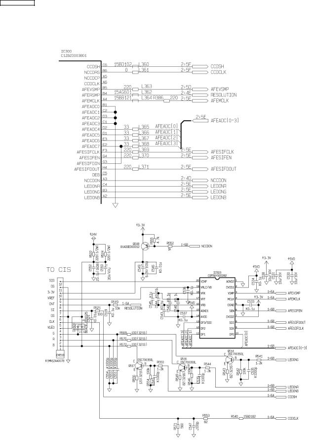
KX-MB1500UCB
6.4.CIS Control Section
The scanning block of this device consists of a control circuit and a CIS (contact image sensor), and AFE(Analog Front End) include A/D Converter.
When an original document is inserted and the start button pressed, pin A3 of IC300 goes to a low level and the transistor Q518 turns on.
This applies voltage to the CIS. The CIS is driven by each of the signals (CCDSH, CCDCLK, Resolution) output from IC300. The original image illuminated by the LED to output an analog image signal.
The analog image signal is input to the AFE on VINP(20pin of IC503) and converted into 16-bit data by the A/D converter inside IC503. Then this signal undergoes digital processing in order to obtain a high-quality image.
24
KX-MB1500UCB
Resolution
The CIS can change the resolution, 300 dpi mode or 600 dpi mode. If RESOLUTION signal is High level, CIS operates 600 dpi mode.
The other case is 300 dpi mode.
Operation |
CIS Resolution |
|
|
300dpi |
600dpi |
COPY |
Photo/Text, Text |
Photo |
PC SCAN |
~300 X 300 |
400 X 400~ |
25
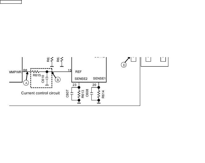
KX-MB1500UCB
6.5.Motor Drive Section
6.5.1.Engine Motor Control Circuit
1. Functions
All driving forces of printer engine part are supplied by tis engine motor.
Engine motor is controlled so as to rotate at constant speed during printing and copying.
2.Block Diagram of Main motor Drive circuit
Main motor drive circuit consists of motor driver IC and Current control circuit. In order to start the motor rotation, following 3 signals are supplied from IC300.
3.Explanation of each circuit
1.Motor driver
IC600 is the constant current, Bi-polar stepping motor drive IC.
This IC can drive up to 2A/phase and support up to 2W1-2 phase excitation.
When "enable" signal (IC600_pin2) becomes "L", motor driver is activated, and motor current are supplied from IC600_pin1, pin18, pin21 and pin22 to drive the motor coil.
Excitation type is selected by the logic level of "MS1"(IC600_pin8) and S2"(IC600_pin9).
The operation of IC600 is shown in below table corresponding to each logic level of enable, MS1, and MS2.
Enable |
MS1 |
MS2 |
Excitation type |
Motor Operation |
(IC600_pin2) |
(IC600_pin8) |
(IC600_pin9) |
|
|
H |
- |
- |
Disable |
Motor stop |
L |
L |
L |
2 Phase Excitation |
Full speed operation |
L |
H |
L |
F1-2 Excitation |
Half speed operation |
L |
L |
H |
W1-2 Excitation |
Not used |
L |
H |
H |
2W1-2 Excitation |
Not used |
After setting the above signals, clock signal is supplied from IC300_pinA12 to IC600_pin14.
Whenever clock signal is supplied, current value and direction supplied to Main motor change according to the excitation type which is determined by above signal levels.
The clock frequency also determines the motor speed.
2.Motor current control circuit
According to the rotation speed, motor current is controlled for appropriate value. In order to control the motor current, Ref voltage of IC600 is controlled.
When Ref voltage is high, motor current is increased, and the voltage is low, motor current is decreased.
For the control of Ref voltage, PWM pulse is supplied from IC300_pinB8. PWM pulse is integrated by R615 and C610.
Consequently PWM pulse is converted to DC voltage.
When duty of PWM pulse is high, Ref voltage is increased and when duty is low, Ref voltage is decreased.
26
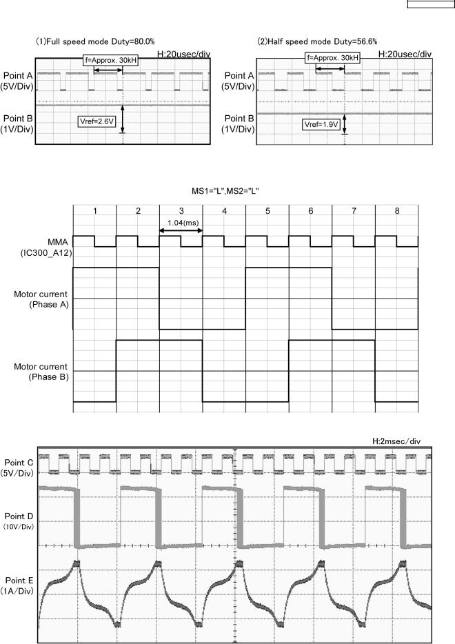
KX-MB1500UCB
4. Explanation of each circuit
5.Timing chart and wave form of Main motors
1.2-2 phase excitation (Full speed)
(1) Timing chart
(2) Wave form
27

KX-MB1500UCB
2. Flat torque 1-2 phase excitation (Half speed)
(1) Timing chart
(2) Wave form
28
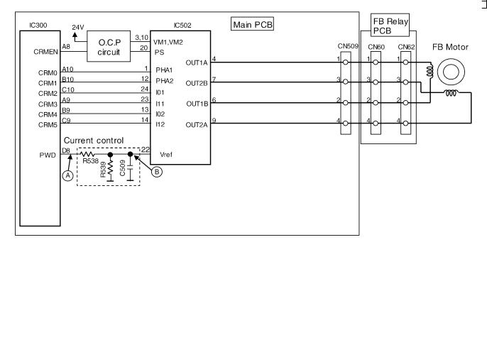
KX-MB1500UCB
6.5.2.FB (Flat bed) motor drive circuit
1.General
FB motor drive circuit consists of "Motor driver", "Motor current control circuit" and "O.C.P(Over Current Protection) circuit" FB motor feeds CIS unit in FB scan, FB copy.
A one step rotation of this motor feeds CIS unit 0.021mm.
2.Block Diagram of Scanner motor Drive circuit
6.5.2.1.Motor driver
Motor driver IC502 can drive motors up to 0.8A/phase and support up to W1-2 phase excitation. When "Power save" signal (IC502_pin20) becomes "H", motor driver is activated.
Stepping pulses are output from IC300 pins A9, B9, C9, A10, B10, and C10.
Frequency and pattern of these pulses determine the motor rotation speed and excitation mode respectively. Corresponding to these pulses, current are supplied from IC502_pin4, pin6, pin7 and pin9 to each motor coil.
6.5.2.2.Motor current control circuit
1.Function
According to the scan speed, motor current is controlled for appropriate value. For example, when scan speed is low, motor has enough driving force.
So to prevent the vibration and noise during motor rotation, motor drive current should be reduced. When scan speed is high, motor needs much driving force. so much current should be supplied. In order to control the motor current, Vref voltage of IC502 is controlled.
When Vref voltage is high, motor current is increased, and the voltage is low, motor current is reduced.
2.Circuit Diagram
Please refer to the circuit diagram shown in the block diagram of FB (Flat bed) motor drive circuit (P.29).
3.Circuit explanation
For the sake of Vref voltage control, PWM pulse is supplied from IC300_pinD8. PWM pulse is integrated by R538, R539 and C764, then converted to DC voltage. This DC voltage is supplied to Vref pin of IC502.
When duty of PWM pulse is high, Vref voltage is increased and when duty is low, Vref voltage is decreased.
29
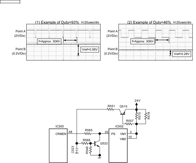
KX-MB1500UCB
4.Timing chart of current control
Following timing charts are the example of Vref voltage corresponding to PWM pulse duty.
6.5.2.3.O.C.P (Over Current Protection) circuit
1.Function
If motor driver can supply more than 15 watts, FB motors may become fire hazards. To prevent the risk of fire, this circuit is provided.
2.Circuit Diagram
3.Circuit explanation
When the current supplied from 24V exceeds 0.44A, the voltage between two registers R575 and R578 becomes more than 0.6V (=0.44A*2.7ohm/2), consequently both Q515 and Q522 turn on.
If Q522 turns on, IC502_pin20 becomes "Low" level.
As a result IC502 is deactivated and motor currents are cut off.
So the current which IC502 can supply is limited to less than 0.44A and the wattage is also limited to less than 10.7W (=0.44A*24V).
By limiting the wattage less than 15W, risk of fire hazard is eliminated.
30
Loading...