


PZU10B1A
Table of contents
 Loading...
NXP PZU10B1A, PZU10B1A/DG, PZU10B2A, PZU10B2A/DG, PZU10B3A Schematic [ru]
...
1. Product profile
1.1 General description
General-purpose Zener diodes in a SOD323 (SC-76) very small Surface-Mounted
Device (SMD) plastic package.
1.2 Features
1.3 Applications
n General regulation functions
1.4 Quick reference data
[1] Pulse test: t
p
≤ 300 µs; δ≤0.02.
[2] t
p
= 100 µs; square wave; T
j
=25°C prior to surge
[3] Device mounted on an FR4 Printed-Circuit Board (PCB), single-sided copper, tin-plated and standard
footprint.
PZUxBA series
Single Zener diodes
Rev. 01 — 19 September 2008 Product data sheet
n Non-repetitive peak reverse power
dissipation: P
ZSM
≤ 40 W
n Low reverse current I
R
range
n Total power dissipation: P
tot
≤ 320 mW n Small plastic package suitable for
surface-mounted design
n Tolerance series:
B: approximately ±5%;
B1, B2, B3: approximately ±2%
n AEC-Q101 qualified
n Wide working voltage range:
nominal 2.4 V to 36 V (E24 range)
Table 1. Quick reference data
Symbol Parameter Conditions Min Typ Max Unit
V
F
forward voltage I
F
= 100 mA
[1]
- - 1.1 V
P
ZSM
non-repetitivepeakreverse
power dissipation
[2]
--40W
P
tot
total power dissipation T
amb
≤ 25 °C
[3]
- - 320 mW
PZUXBA_SER_1 © NXP B.V. 2008. All rights reserved.
Product data sheet Rev. 01 — 19 September 2008 2 of 14
NXP Semiconductors
PZUxBA series
Single Zener diodes
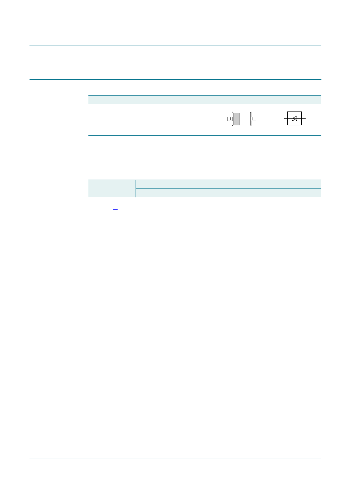
2. Pinning information
[1] The marking bar indicates the cathode.
3. Ordering information
[1] The series consists of 97 types with nominal working voltages from 2.4 V to 36 V.
[2] /DG: halogen-free
Table 2. Pinning
Pin Description Simplified outline Graphic symbol
1 cathode
[1]
2 anode
21
006aaa152
2
1
Table 3. Ordering information
Type number Package
Name Description Version
PZU2.4BA to
PZU36BA
[1]
SC-76 plastic surface-mounted package; 2 leads SOD323
PZU2.4BA/DG to
PZU36BA/DG
[1][2]

PZUXBA_SER_1 © NXP B.V. 2008. All rights reserved.
Product data sheet Rev. 01 — 19 September 2008 3 of 14
NXP Semiconductors
PZUxBA series
Single Zener diodes
4. Marking
[1] * = B: tolerance series B, approximately ±5%
* = B1, B2, B3: tolerance series B1, B2, B3: approximately ±2%
Table 4. Marking codes
Type number
[1]
Marking code Type number
[1]
Marking code
B B1 B2 B3 B B1 B2 B3
PZU2.4*A X8 - - - PZU2.4*A/DG Y8 - - -
PZU2.7*A X9 XA XB - PZU2.7*A/DG Y9 YA YB -
PZU3.0*A XT XU XV - PZU3.0*A/DG YT YU YV -
PZU3.3*A XW XX XY - PZU3.3*A/DG YW YX YY -
PZU3.6*A XZ MC MD - PZU3.6*A/DG YZ NC ND -
PZU3.9*A ME MF MG - PZU3.9*A/DG NE NF NG -
PZU4.3*A MM MN MP MR PZU4.3*A/DG NM NN NP NR
PZU4.7*A MS MT MU MV PZU4.7*A/DG NS NT NU NV
PZU5.1*A MW MX MY MZ PZU5.1*A/DG NW NX NY NZ
PZU5.6*A LF LG LH LK PZU5.6*A/DG RF RG RH RK
PZU6.2*A LL LM LN LP PZU6.2*A/DG RL RM RN RP
PZU6.8*A LR LS LT LU PZU6.8*A/DG RR RS RT RU
PZU7.5*A LV LW LX LY PZU7.5*A/DG RV RW RX RY
PZU8.2*A LZ CR CS CT PZU8.2*A/DG RZ ER ES ET
PZU9.1*A CU CV CW CX PZU9.1*A/DG EU EV EW EX
PZU10*A VA VB VC VD PZU10*A/DG WA WB WC WD
PZU11*A VE VF VG VH PZU11*A/DG WE WF WG WH
PZU12*A VK VL VM VN PZU12*A/DG WK WL WM WN
PZU13*A VP VR VS VT PZU13*A/DG WP WR WS WT
PZU14*A - - VU - PZU14*A/DG - - WU -
PZU15*A VV VW VX VY PZU15*A/DG WV WW WX WY
PZU16*A VZ X1 X2 X3 PZU16*A/DG WZ Y1 Y2 Y3
PZU18*A X4 X5 X6 X7 PZU18*A/DG Y4 Y5 Y6 Y7
PZU20*A XC XD XE XF PZU20*A/DG YC YD YE YF
PZU22*A XG XH XK XL PZU22*A/DG YG YH YK YL
PZU24*A XM XN XP XR PZU24*A/DG YM YN YP YR
PZU27*A XS - - - PZU27*A/DG YS - - -
PZU30*A MH - - - PZU30*A/DG NH - - -
PZU33*A MK - - - PZU33*A/DG NK - - -
PZU36*A ML - - - PZU36*A/DG NL - - -

PZUXBA_SER_1 © NXP B.V. 2008. All rights reserved.
Product data sheet Rev. 01 — 19 September 2008 4 of 14
NXP Semiconductors
PZUxBA series
Single Zener diodes
5. Limiting values
[1] t
p
= 100 µs; square wave; T
j
=25°C prior to surge
[2] Device mounted on an FR4 PCB, single-sided copper, tin-plated and standard footprint.
[3] Device mounted on an FR4 PCB, single-sided copper, tin-plated, mounting pad for cathode 1 cm
2
.
6. Thermal characteristics
[1] Device mounted on an FR4 PCB, single-sided copper, tin-plated and standard footprint.
[2] Device mounted on an FR4 PCB, single-sided copper, tin-plated, mounting pad for cathode 1 cm
2
.
[3] Soldering point of cathode tab.
7. Characteristics
[1] Pulse test: t
p
≤ 300 µs; δ≤0.02.
Table 5. Limiting values
In accordance with the Absolute Maximum Rating System (IEC 60134).
Symbol Parameter Conditions Min Max Unit
I
F
forward current - 200 mA
I
ZSM
non-repetitive peak reverse
current
[1]
- see
Table 8
and
9
P
ZSM
non-repetitive peak reverse
power dissipation
[1]
-40W
P
tot
total power dissipation T
amb
≤ 25 °C
[2]
- 320 mW
[3]
- 490 mW
T
j
junction temperature - 150 °C
T
amb
ambient temperature −55 +150 °C
T
stg
storage temperature −65 +150 °C
Table 6. Thermal characteristics
Symbol Parameter Conditions Min Typ Max Unit
R
th(j-a)
thermal resistance from
junction to ambient
in free air
[1]
- - 390 K/W
[2]
- - 255 K/W
R
th(j-sp)
thermal resistance from
junction to solder point
[3]
--55K/W
Table 7. Characteristics
T
j
=25
°
C unless otherwise specified.
Symbol Parameter Conditions Min Typ Max Unit
V
F
forward voltage
[1]
I
F
= 10 mA - - 0.9 V
I
F
= 100 mA - - 1.1 V

PZUXBA_SER_1 © NXP B.V. 2008. All rights reserved.
Product data sheet Rev. 01 — 19 September 2008 5 of 14
NXP Semiconductors
PZUxBA series
Single Zener diodes
[1] f = 1 MHz; V
R
=0V
[2] t
p
= 100 µs; square wave; T
j
=25°C prior to surge
Table 8. Characteristics per type; PZU2.4BA to PZU5.6B3A and PZU2.4BA/DG to PZU5.6B3A/DG
T
j
=25
°
C unless otherwise specified.
PZUxBA Sel Working
voltage
V
Z
(V)
Differentialresistance
r
dif
(Ω)
Reverse
current
I
R
(µA)
Temperature
coefficient
S
Z
(mV/K)
Diode
capacitance
C
d
(pF)
[1]
Non-repetitive
peak reverse
current
I
ZSM
(A)
[2]
I
Z
=5mA I
Z
= 0.5 mA I
Z
=5mA I
Z
=5mA
Min Max Max Max Max V
R
(V) Typ Max Max
2.4 B 2.3 2.6 1000 100 50 1 −1.6 450 8
2.7 B 2.5 2.9 1000 100 20 1 −2.0 440 8
B1 2.5 2.75
B2 2.65 2.9
3.0 B 2.8 3.2 1000 95 10 1 −2.1 425 8
B1 2.8 3.05
B2 2.95 3.2
3.3 B 3.1 3.5 1000 95 5 1 −2.4 410 8
B1 3.1 3.35
B2 3.25 3.5
3.6 B 3.4 3.8 1000 90 5 1 −2.4 390 8
B1 3.4 3.65
B2 3.55 3.8
3.9 B 3.7 4.1 1000 90 3 1 −2.5 370 8
B1 3.7 3.97
B2 3.87 4.10
4.3 B 4.01 4.48 1000 90 3 1 −2.5 350 8
B1 4.01 4.21
B2 4.15 4.34
B3 4.28 4.48
4.7 B 4.42 4.9 800 80 2 1 −1.4 325 8
B1 4.42 4.61
B2 4.55 4.75
B3 4.69 4.9
5.1 B 4.84 5.37 250 60 2 1.5 0.3 300 5.5
B1 4.84 5.04
B2 4.98 5.2
B3 5.14 5.37
5.6 B 5.31 5.92 100 40 1 2.5 1.9 275 5.5
B1 5.31 5.55
B2 5.49 5.73
B3 5.67 5.92
Loading...