


 Loading...
NXP 74HC595BQ, 74HC595D, 74HC595DB, 74HC595N, 74HC595PW Schematics
... 74HC595; 74HCT595
8-bit serial-in, serial or parallel-out shift register with output latches; 3-state
Rev. 6 — 12 December 2011 |
Product data sheet |
1. General description
The 74HC595; 74HCT595 are high-speed Si-gate CMOS devices and are pin compatible with Low-power Schottky TTL (LSTTL). They are specified in compliance with JEDEC standard No. 7A.
The 74HC595; 74HCT595 are 8-stage serial shift registers with a storage register and 3-state outputs. The registers have separate clocks.
Data is shifted on the positive-going transitions of the shift register clock input (SHCP). The data in each register is transferred to the storage register on a positive-going transition of the storage register clock input (STCP). If both clocks are connected together, the shift register will always be one clock pulse ahead of the storage register.
The shift register has a serial input (DS) and a serial standard output (Q7S) for cascading. It is also provided with asynchronous reset (active LOW) for all 8 shift register stages. The storage register has 8 parallel 3-state bus driver outputs. Data in the storage register appears at the output whenever the output enable input (OE) is LOW.
2.Features and benefits
8-bit serial input
8-bit serial or parallel output
Storage register with 3-state outputs
Shift register with direct clear
100 MHz (typical) shift out frequency
ESD protection:
HBM JESD22-A114F exceeds 2000 V
MM JESD22-A115-A exceeds 200 V
Multiple package options
Specified from 40 C to +85 C and from 40 C to +125 C
3.Applications
Serial-to-parallel data conversion
Remote control holding register

NXP Semiconductors |
74HC595; 74HCT595 |
|
8-bit serial-in, serial or parallel-out shift register with output latches; |
|
3-state |
4. Ordering information
Table 1. Ordering information
Type number |
Package |
|
|
|
|
|
|
|
|
|
Temperature range |
Name |
Description |
Version |
|
40 C to +125 C |
|
|
|
74HC595N |
DIP16 |
plastic dual in-line package; 16 leads (300 mil) |
SOT38-4 |
|
74HCT595N |
40 C to +125 C |
|
|
|
74HC595D |
SO16 |
plastic small outline package; 16 leads; |
SOT109-1 |
|
|
|
|
body width 3.9 mm |
|
74HCT595D |
40 C to +125 C |
|
|
|
|
|
|
||
74HC595DB |
SSOP16 |
plastic shrink small outline package; 16 leads; |
SOT338-1 |
|
|
|
|
body width 5.3 mm |
|
74HCT595DB |
40 C to +125 C |
|
|
|
|
|
|
||
74HC595PW |
TSSOP16 |
plastic thin shrink small outline package; 16 leads; |
SOT403-1 |
|
|
|
|
body width 4.4 mm |
|
74HCT595PW |
40 C to +125 C |
|
|
|
|
|
|
||
74HC595BQ |
DHVQFN16 |
plastic dual in-line compatible thermal enhanced |
SOT763-1 |
74HCT595BQ |
very thin quad flat package; no leads; 16 terminals; |
|||
body 2.5 |
3.5 |
0.85 mm |
||
|
||||
5. Functional diagram
14 |
DS |
|
|
|
|
|
|
|
|
|
|
|
|
||||
11 |
SHCP |
|
8-STAGE SHIFT REGISTER |
|
|
|
|
|
|||||||||
|
|
|
|
|
|
|
|
|
|
|
|||||||
10 |
|
|
|
|
|
|
|
|
|
|
|||||||
MR |
|
|
|
|
|
|
|||||||||||
|
|
|
|
|
|
|
|
|
|
|
|
||||||
|
|
|
|
|
|
|
|
|
|
|
|
|
|
|
|
|
|
|
|
|
|
|
|
|
|
|
|
|
|
|
|
|
|
|
|
12 |
STCP |
|
|
|
|
|
|
|
|
|
|
Q7S |
9 |
|
|||
|
8-BIT STORAGE REGISTER |
|
|
|
|||||||||||||
|
|
|
|
|
|
|
|
|
|
|
|
|
|
|
|
|
|
13 |
|
|
|
|
|
|
|
|
|
|
|
|
|
|
|
|
|
|
|
|
|
|
|
|
|
|
|
|
|
|
|
|
|
|
|
|
|
|
|
|
|
|
|
|
|
|
|
|
|
|
|
||
OE |
|
|
3-STATE OUTPUTS |
|
|
|
|
|
|
||||||||
|
|
|
|
|
|
|
|
|
|
|
|
|
|||||
|
|
|
|
|
|
|
|
|
|
|
|
|
|||||
|
|
|
|
|
|
|
|
|
|
|
|
|
|
|
|
|
|
|
|
|
|
|
|
Q0 |
Q1 |
Q2 |
Q3 |
Q4 |
Q5 |
Q6 |
Q7 |
|
|
|
|
|
|
|
|
|
|
|
|
|
|
|
|
|
|
|
|
|
|
|
|
|
|
|
|
15 |
1 |
2 |
3 |
4 |
5 |
6 |
7 |
|
mna554 |
||
Fig 1. Functional diagram
74HC_HCT595 |
All information provided in this document is subject to legal disclaimers. |
© NXP B.V. 2011. All rights reserved. |
Product data sheet |
Rev. 6 — 12 December 2011 |
2 of 24 |

NXP Semiconductors |
74HC595; 74HCT595 |
8-bit serial-in, serial or parallel-out shift register with output latches; 3-state
|
|
|
|
|
13 |
|
|
EN3 |
|
|
|
|
|
|
12 |
|
|
|
|
|
11 |
12 |
|
|
|
|
C2 |
|
|
|
|
|
|
|
|
|
|||
|
SHCP |
STCP |
|
|
10 |
R |
|
SRG8 |
|
|
|
|
11 |
|
|
||||
|
|
Q7S |
9 |
|
C1/ |
|
|
||
|
|
15 |
|
|
|
|
|||
|
|
Q0 |
|
14 |
|
|
|
15 |
|
|
|
1 |
|
1D |
|
2D |
|||
|
|
|
|
|
|||||
|
|
Q1 |
|
|
|
3 |
|||
|
|
2 |
|
|
|
|
|
1 |
|
|
|
|
|
|
|
|
|
||
|
|
Q2 |
|
|
|
|
|
2 |
|
|
14 |
3 |
|
|
|
|
|
||
|
|
|
|
|
|
|
|||
|
Q3 |
|
|
|
|
|
|
||
|
DS |
4 |
|
|
|
|
|
3 |
|
|
|
Q4 |
|
|
|
|
|
4 |
|
|
|
5 |
|
|
|
|
|
||
|
|
|
|
|
|
|
|
||
|
|
Q5 |
|
|
|
|
|
5 |
|
|
|
6 |
|
|
|
|
|
||
|
|
|
|
|
|
|
|
||
|
|
Q6 |
|
|
|
|
|
6 |
|
|
|
7 |
|
|
|
|
|
||
|
|
|
|
|
|
|
|
||
|
|
Q7 |
|
|
|
|
|
7 |
|
|
|
|
|
|
|
|
|
||
|
|
|
|
|
|
|
|
|
|
|
MR |
OE |
|
|
|
|
|
|
9 |
|
|
|
|
|
|
|
|
|
|
|
10 |
13 |
mna552 |
|
|
|
|
|
mna553 |
|
|
|
|
|
|
|
|
||
Fig 2. |
Logic symbol |
|
|
|
Fig 3. IEC logic symbol |
|
|||
|
|
STAGE 0 |
|
STAGES 1 TO 6 |
|
STAGE 7 |
|
||
|
DS |
D Q |
D |
Q |
|
D Q |
Q7S |
||
|
|
FF0 |
|
|
|
|
FF7 |
|
|
|
|
CP |
|
|
|
|
CP |
|
|
|
|
R |
|
|
|
|
|
R |
|
|
SHCP |
|
|
|
|
|
|
|
|
|
MR |
|
|
|
|
|
|
|
|
|
|
D |
Q |
|
|
|
D |
Q |
|
|
|
LATCH |
|
|
|
LATCH |
|
||
|
|
CP |
|
|
|
|
CP |
|
|
|
STCP |
|
|
|
|
|
|
|
|
|
OE |
|
|
|
|
|
|
|
|
|
|
|
Q0 |
Q1 Q2 Q3 Q4 Q5 Q6 |
|
|
Q7 |
mna555 |
|
|
|
|
|
|
|
||||
Fig 4. Logic diagram
74HC_HCT595 |
All information provided in this document is subject to legal disclaimers. |
© NXP B.V. 2011. All rights reserved. |
Product data sheet |
Rev. 6 — 12 December 2011 |
3 of 24 |
NXP Semiconductors |
74HC595; 74HCT595 |
|
8-bit serial-in, serial or parallel-out shift register with output latches; |
|
3-state |
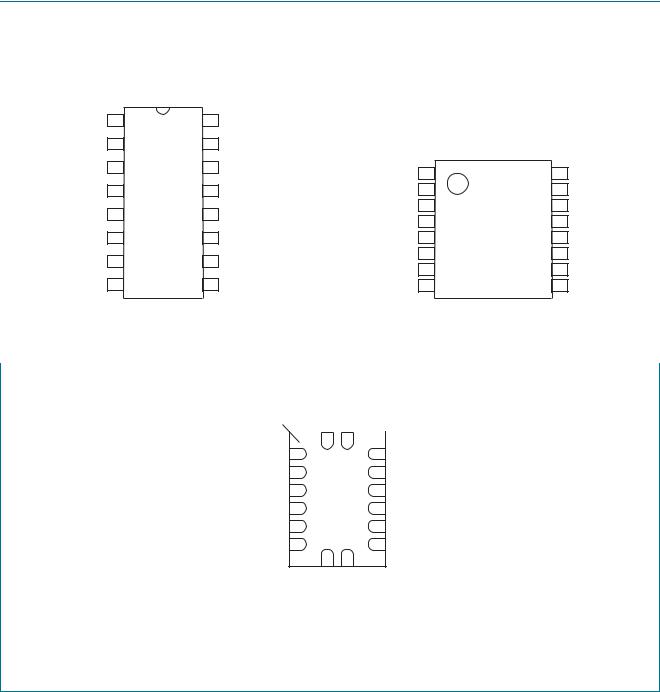
6.Pinning information
6.1Pinning
|
|
|
74HC595 |
|
|
|
|
|
|
|
|
|
|
|
|
|
|
|
|
|
|
|
|
74HCT595 |
|
|
|
|
|
|
|
|
|
|
|
|
|
|
|
|
|
Q1 |
1 |
|
VCC |
|
|
|
|
|
|
|
|
|
|
|
74HC595 |
|
|
|||
|
16 |
|
|
|
|
|
|
|
|
|
|
|
|
|
||||||
|
|
|
|
|
|
|
|
|
|
|
|
|
|
|
|
|
|
|
|
|
Q2 |
2 |
|
15 |
Q0 |
|
|
|
|
|
|
|
|
|
|
|
74HCT595 |
|
|
||
Q3 |
3 |
|
14 |
DS |
|
|
|
|
|
|
|
|
Q1 |
1 |
16 |
VCC |
||||
|
|
|
|
|
|
|
|
|
|
|
|
|
|
|
||||||
Q4 |
4 |
|
13 |
OE |
|
|
|
|
|
|
|
|
|
|
Q2 |
2 |
15 |
Q0 |
||
Q5 |
5 |
|
12 |
STCP |
|
|
|
|
|
|
|
|
Q3 |
3 |
14 |
DS |
||||
|
|
|
|
|
|
|
|
|
|
|
4 |
13 |
|
|
||||||
|
|
|
|
|
|
|
|
|
Q4 |
OE |
||||||||||
|
|
|
|
|
|
|
|
|
|
|
|
|
|
|
||||||
Q6 |
6 |
|
11 |
SHCP |
|
|
|
|
|
|
|
|
Q5 |
5 |
12 |
STCP |
||||
|
7 |
|
10 |
|
|
|
|
|
|
|
|
|
|
|
Q6 |
6 |
11 |
SHCP |
||
Q7 |
|
MR |
|
|
|
|
|
|
||||||||||||
|
|
|
|
|
|
|
|
|
Q7 |
7 |
10 |
|
|
|||||||
|
|
|
|
|
|
|
|
|
|
|
|
|
|
|
MR |
|
||||
GND |
8 |
|
9 |
Q7S |
|
|
|
|
|
|
|
|
GND |
8 |
9 |
Q7S |
||||
|
|
|
001aao241 |
|
|
|
|
|
|
|
|
|
|
|
|
|
|
001aao242 |
|
|
|
|
|
|
|
|
|
|
|
|
|
|
|
|
|
|
|
|
|
||
Fig 5. Pin configuration DIP16, SO16 |
|
|
|
|
Fig 6. Pin configuration SSOP16, TSSOP16 |
|||||||||||||||
|
|
|
|
|
|
|
|
|
|
|
|
|
|
|
|
|
|
|
|
|
|
|
|
|
|
|
|
|
|
|
|
|
|
|
|
|
|
|
|
||
|
|
|
|
|
|
|
|
74HC595 |
|
|
|
|
|
|
|
|
||||
|
|
|
|
|
|
|
|
74HCT595 |
|
|
|
|
|
|
|
|
||||
|
|
|
|
|
terminal 1 |
|
|
Q1 |
CC |
|
|
|
|
|
|
|
|
|||
|
|
|
|
|
|
|
V |
|
|
|
|
|
|
|
|
|||||
|
|
|
|
|
|
|
|
|
|
|
|
|
|
|
|
|
|
|
||
|
|
|
|
index area |
|
|
|
|
|
|
|
|
|
|
|
|
|
|
||
|
|
|
|
|
|
|
|
1 |
16 |
|
|
|
|
|
|
|
|
|
||
|
|
|
|
|
|
Q2 |
2 |
|
|
|
15 |
|
Q0 |
|
|
|
|
|||
|
|
|
|
|
|
Q3 |
3 |
|
|
|
|
14 |
|
DS |
|
|
|
|
||
|
|
|
|
|
|
Q4 |
4 |
|
|
|
|
13 |
|
|
|
|
|
|
||
|
|
|
|
|
|
|
|
|
|
|
OE |
|
|
|
|
|
||||
|
|
|
|
|
|
Q5 |
5 |
|
|
|
|
12 |
|
STCP |
|
|
|
|
||
|
|
|
|
|
|
Q6 |
6 |
|
GND(1) |
11 |
|
SHCP |
|
|
|
|
||||
|
|
|
|
|
|
Q7 |
7 |
|
|
|
10 |
|
|
|
|
|
|
|||
|
|
|
|
|
|
|
|
|
|
|
MR |
|
|
|
|
|
||||
8
GND
Transparent
Q7S 9
top view
001aao243
(1)This is not a supply pin, the substrate is attached to this pad using conductive die attach material. There is no electrical or mechanical requirement to solder this pad however if it is soldered the solder land should remain floating or be connected to GND.
Fig 7. Pin configuration for DHVQFN16
74HC_HCT595 |
All information provided in this document is subject to legal disclaimers. |
© NXP B.V. 2011. All rights reserved. |
Product data sheet |
Rev. 6 — 12 December 2011 |
4 of 24 |

NXP Semiconductors |
|
|
|
|
74HC595; 74HCT595 |
||||||||||||||
|
|
|
|
|
|
|
|
|
|
|
|
|
|
|
8-bit serial-in, serial or parallel-out shift register with output latches; |
||||
|
|
|
|
|
|
|
|
|
|
|
|
|
|
|
|
|
|
|
3-state |
|
|
|
|
|
|
6.2 |
|
|
Pin description |
|
|
|
|
||||||
Table 2. |
|
Pin description |
|
|
|
|
|
|
|||||||||||
|
|
|
|
|
|
|
|
|
|
|
|
|
|
|
|
|
|
|
|
|
Symbol |
|
|
|
|
Pin |
|
Description |
|
|
|
||||||||
|
Q1 |
|
|
|
|
|
1 |
|
|
parallel data output 1 |
|||||||||
|
|
|
|
|
|
|
|
|
|
|
|
|
|
|
|
|
|
||
|
Q2 |
|
|
|
|
|
2 |
|
|
parallel data output 2 |
|||||||||
|
|
|
|
|
|
|
|
|
|
|
|
|
|
|
|
|
|
||
|
Q3 |
|
|
|
|
|
3 |
|
|
parallel data output 3 |
|||||||||
|
|
|
|
|
|
|
|
|
|
|
|
|
|
|
|
|
|
||
|
Q4 |
|
|
|
|
|
4 |
|
|
parallel data output 4 |
|||||||||
|
|
|
|
|
|
|
|
|
|
|
|
|
|
|
|
|
|
||
|
Q5 |
|
|
|
|
|
5 |
|
|
parallel data output 5 |
|||||||||
|
|
|
|
|
|
|
|
|
|
|
|
|
|
|
|
|
|
||
|
Q6 |
|
|
|
|
|
6 |
|
|
parallel data output 6 |
|||||||||
|
|
|
|
|
|
|
|
|
|
|
|
|
|
|
|
|
|
||
|
Q7 |
|
|
|
|
|
7 |
|
|
parallel data output 7 |
|||||||||
|
|
|
|
|
|
|
|
|
|
|
|
|
|
|
|
|
|
||
|
GND |
|
|
|
|
|
8 |
|
|
ground (0 V) |
|
|
|
||||||
|
|
|
|
|
|
|
|
|
|
|
|
|
|
|
|
|
|
||
|
Q7S |
|
|
|
|
|
9 |
|
|
serial data output |
|||||||||
|
|
|
|
|
|
|
|
|
|
|
|
|
|
|
|
|
|
|
|
|
|
|
|
|
|
|
|
|
|
10 |
|
|
master reset (active LOW) |
||||||
|
MR |
|
|
|
|
|
|
|
|
|
|||||||||
|
|
|
|
|
|
|
|
|
|
|
|
|
|
|
|
|
|
||
|
SHCP |
|
|
|
|
|
11 |
|
|
shift register clock input |
|||||||||
|
|
|
|
|
|
|
|
|
|
|
|
|
|
|
|
|
|
||
|
STCP |
|
|
|
|
|
12 |
|
|
storage register clock input |
|||||||||
|
|
|
|
|
|
|
|
|
|
|
|
|
|
|
|
|
|
||
|
|
|
|
|
|
|
|
|
|
13 |
|
|
output enable input (active LOW) |
||||||
|
OE |
|
|
|
|
|
|
|
|
|
|||||||||
|
|
|
|
|
|
|
|
|
|
|
|
|
|
|
|
|
|
||
|
DS |
|
|
|
|
|
14 |
|
|
serial data input |
|
|
|
||||||
|
|
|
|
|
|
|
|
|
|
|
|
|
|
|
|
|
|
||
|
Q0 |
|
|
|
|
|
15 |
|
|
parallel data output 0 |
|||||||||
|
|
|
|
|
|
|
|
|
|
|
|
|
|
|
|
|
|
||
|
VCC |
|
|
|
|
|
16 |
|
|
supply voltage |
|
|
|
||||||
7. Functional description |
|
|
|
|
|||||||||||||||
|
|
|
|
|
|
|
|
|
|
|
|
|
|
|
|
|
|
|
|
Table 3. |
|
Function table[1] |
|
|
|
|
|
|
|||||||||||
|
Control |
|
|
|
|
|
|
|
|
|
Input |
Output |
|
Function |
|||||
|
SHCP |
|
STCP |
|
OE |
|
|
|
MR |
|
DS |
Q7S |
Qn |
|
|
|
|||
|
|
|
|
|
|
|
|
|
|
|
|
|
|
||||||
|
X |
X |
|
|
L |
|
|
L |
X |
L |
NC |
a LOW-level on |
MR |
only affects the shift registers |
|||||
|
X |
|
|
|
L |
|
|
L |
X |
L |
L |
empty shift register loaded into storage register |
|||||||
X |
X |
|
|
H |
|
|
L |
X |
L |
Z |
shift register clear; parallel outputs in high-impedance OFF-state |
||||||||
|
X |
|
L |
|
H |
H |
Q6S |
NC |
logic HIGH-level shifted into shift register stage 0. Contents of all |
||||||||||
|
|
|
|
|
|
|
|
|
|
|
|
|
|
|
|
|
shift register stages shifted through, e.g. previous state of stage 6 |
||
|
|
|
|
|
|
|
|
|
|
|
|
|
|
|
|
|
(internal Q6S) appears on the serial output (Q7S). |
||
X |
|
L |
|
H |
X |
NC |
QnS |
contents of shift register stages (internal QnS) are transferred to |
|||||||||||
|
|
|
|
|
|
|
|
|
|
|
|
|
the storage register and parallel output stages |
||||||
|
L |
|
H |
X |
Q6S |
QnS |
contents of shift register shifted through; previous contents of the |
||||||||||||
shift register is transferred to the storage register and the parallel output stages
[1]H = HIGH voltage state;
L = LOW voltage state;
= LOW-to-HIGH transition; X = don’t care;
NC = no change;
Z = high-impedance OFF-state.
74HC_HCT595 |
All information provided in this document is subject to legal disclaimers. |
© NXP B.V. 2011. All rights reserved. |
Product data sheet |
Rev. 6 — 12 December 2011 |
5 of 24 |

NXP Semiconductors |
|
|
|
|
|
|
|
|
|
|
|
|
|
|
|
|
|
74HC595; 74HCT595 |
||||||||||||||||||||||
|
|
|
|
|
|
|
|
|
|
|
|
|
8-bit serial-in, serial or parallel-out shift register with output latches; |
|||||||||||||||||||||||||||
|
|
|
|
|
|
|
|
|
|
|
|
|
|
|
|
|
|
|
|
|
|
|
|
|
|
|
|
|
|
|
|
|
|
|
|
|
|
|
|
3-state |
|
|
|
|
|
|
|
|
|
|
|
|
|
|
|
|
|
|
|
|
|
|
|
|
|
|
|
|
|
|
|
|
|
|
|
|
|
|
|
|
|
|
|
|
|
|
|
|
|
|
|
|
|
|
|
|
|
|
|
|
|
|
|
|
|
|
|
|
|
|
|
|
|
|
|
|
|
|
|
|
||
SHCP |
|
|
|
|
|
|
|
|
|
|
|
|
|
|
|
|
|
|
|
|
|
|
|
|
|
|
|
|
|
|
|
|
|
|
|
|
|
|
||
|
DS |
|
|
|
|
|
|
|
|
|
|
|
|
|
|
|
|
|
|
|
|
|
|
|
|
|
|
|
|
|
|
|
|
|
||||||
|
|
|
|
|
|
|
|
|
|
|
|
|
|
|
|
|
|
|
|
|
|
|
|
|
|
|
|
|
|
|
|
|
|
|||||||
|
|
|
|
|
|
|
|
|
|
|
|
|
|
|
|
|
|
|
|
|
|
|
|
|
|
|
|
|
|
|
|
|
|
|||||||
|
|
|
|
|
|
|
|
|
|
|
|
|
|
|
|
|
|
|
|
|
|
|
|
|
|
|
|
|
|
|
|
|
|
|
|
|
|
|
|
|
STCP |
|
|
|
|
|
|
|
|
|
|
|
|
|
|
|
|
|
|
|
|
|
|
|
|
|
|
|
|
|
|
|
|
|
|||||||
|
|
|
|
|
|
|
|
|
|
|
|
|
|
|
|
|
|
|
|
|
|
|
|
|
|
|
|
|
|
|
|
|||||||||
|
|
|
|
|
|
|
|
|
|
|
|
|
|
|
|
|
|
|
|
|
|
|
|
|
|
|
|
|
|
|
|
|||||||||
|
|
|
|
|
|
|
|
|
|
|
|
|
|
|
|
|
|
|
|
|
|
|
|
|
|
|
|
|
|
|
|
|||||||||
|
|
|
|
|
|
|
|
|
|
|
|
|
|
|
|
|
|
|
|
|
|
|
|
|
|
|
|
|
|
|
|
|
|
|
|
|
||||
|
|
|
|
|
|
|
|
|
|
|
|
|
|
|
|
|
|
|
|
|
|
|
|
|
|
|
|
|
|
|
|
|
|
|
|
|
|
|
|
|
|
|
|
|
|
|
|
|
|
|
|
|
|
|
|
|
|
|
|
|
|
|
|
|
|
|
|
|
|
|
|
|
|
|
|
|
|
|
|
|
|
|
MR |
|
|
|
|
|
|
|
|
|
|
|
|
|
|
|
|
|
|
|
|
|
|
|
|
|
|
|
|
|
|
|
|
|
|
|
|
|||
|
|
|
|
|
|
|
|
|
|
|
|
|
|
|
|
|
|
|
|
|
|
|
|
|
|
|
|
|
|
|
|
|
|
|
||||||
|
|
|
|
|
|
|
|
|
|
|
|
|
|
|
|
|
|
|
|
|
|
|
|
|
|
|
|
|
|
|
|
|
|
|
|
|
||||
|
|
|
|
|
|
|
|
|
|
|
|
|
|
|
|
|
|
|
|
|
|
|
|
|
|
|
|
|
|
|
|
|
|
|
|
|
|
|
|
|
|
|
|
|
|
|
|
|
|
|
|
|
|
|
|
|
|
|
|
|
|
|
|
|
|
|
|
|
|
|
|
|
|
|
|
|
|
|
|
|
|
|
OE |
|
|
|
|
|
|
|
|
|
|
|
|
|
|
|
|
|
|
|
|
|
|
|
|
|
|
|
|
|
|
|
|
|
|
|
||||
|
|
|
|
|
|
|
|
|
|
|
|
|
|
|
|
|
|
|
|
|
|
|
|
|
|
|
|
|
|
|
|
|||||||||
|
|
|
|
|
|
|
|
|
|
|
|
|
|
|
|
|
|
|
|
|
|
|
|
|
|
|
|
|
|
|
||||||||||
|
Q0 |
|
|
|
|
|
|
|
|
|
|
|
|
|
|
|
|
|
|
|
|
|
|
Z-state |
|
|
||||||||||||||
|
|
|
|
|
|
|
|
|
|
|
|
|
|
|
|
|
|
|
|
|
|
|
|
|
||||||||||||||||
|
Q1 |
|
|
|
|
|
|
|
|
|
|
|
|
|
|
|
|
|
|
|
|
|
|
Z-state |
|
|
||||||||||||||
|
|
|
|
|
|
|
|
|
|
|
|
|
|
|
|
|
|
|
|
|
|
|
||||||||||||||||||
|
|
|
|
|
|
|
|
|
|
|
|
|
|
|
|
|
|
|
|
|
|
|
|
|
|
|
|
|
|
|
|
|
|
|||||||
|
Q6 |
|
|
|
|
|
|
|
|
|
|
|
|
|
|
|
|
|
|
|
|
|
|
Z-state |
|
|
||||||||||||||
|
|
|
|
|
|
|
|
|
|
|
|
|
|
|
|
|
|
|
|
|
|
|
|
|
||||||||||||||||
|
|
|
|
|
|
|
|
|
|
|
|
|
|
|
|
|
|
|
|
|
|
|
|
|
||||||||||||||||
|
|
|
|
|
|
|
|
|
|
|
|
|
|
|
|
|
|
|
|
|
|
|
|
|
|
|
|
|
|
|
|
|
|
|
|
|
|
|
|
|
|
Q7 |
|
|
|
|
|
|
|
|
|
|
|
|
|
|
|
|
|
|
|
|
|
|
Z-state |
|
|
||||||||||||||
|
|
|
|
|
|
|
|
|
|
|
|
|
|
|
|
|
|
|
|
|
|
|
|
|
||||||||||||||||
|
|
|
|
|
|
|
|
|
|
|
|
|
|
|
|
|
|
|
|
|
|
|
|
|
||||||||||||||||
|
|
|
|
|
|
|
|
|
|
|
|
|
|
|
|
|
|
|
|
|
|
|
|
|
|
|
|
|
|
|
|
|
|
|
|
|
|
|
|
|
|
|
|
|
|
|
|
|
|
|
|
|
|
|
|
|
|
|
|
|
|
|
|
|
|
|
|
|
|
|
|
|
|
|
|
|
|||||
Q7S |
|
|
|
|
|
|
|
|
|
|
|
|
|
|
|
|
|
|
|
|
|
|
|
|
|
|
|
|
|
|
|
|
|
|
|
|
||||
|
|
|
|
|
|
|
|
|
|
|
|
|
|
|
|
|
|
|
|
|
|
|
|
|
|
|
|
|
|
|
|
|
|
|
|
|||||
|
|
|
|
|
|
|
|
|
|
|
|
|
|
|
|
|
|
|
|
|
|
|
|
|
|
|
|
|
|
|
|
|
|
|
|
|
|
mna556 |
||
Fig 8. Timing diagram
8. Limiting values
Table 4. Limiting values
In accordance with the Absolute Maximum Rating System (IEC 60134). Voltages are referenced to GND (ground = 0 V).
Symbol |
Parameter |
Conditions |
Min |
Max |
Unit |
|
|
|
0.5 |
|
|
VCC |
supply voltage |
VI < 0.5 V or VI > VCC + 0.5 V |
+7 |
V |
|
IIK |
input clamping current |
- |
20 |
mA |
|
IOK |
output clamping current |
VO < 0.5 V or VO > VCC + 0.5 V |
- |
20 |
mA |
IO |
output current |
VO = 0.5 V to (VCC + 0.5 V) |
|
25 |
|
|
|
pin Q7S |
- |
mA |
|
|
|
pins Qn |
- |
35 |
mA |
ICC |
supply current |
|
- |
70 |
mA |
IGND |
ground current |
|
70 |
- |
mA |
Tstg |
storage temperature |
|
65 |
+150 |
C |
Ptot |
total power dissipation |
|
|
|
|
DIP16 package |
[1] |
- |
750 |
mW |
SO16 package |
[2] |
- |
500 |
mW |
SSOP16 package |
[3] |
- |
500 |
mW |
TSSOP16 package |
[3] |
- |
500 |
mW |
DHVQFN16 package |
[4] |
- |
500 |
mW |
[1]For DIP16 package: Ptot derates linearly with 12 mW/K above 70 C.
[2]For SO16 package: Ptot derates linearly with 8 mW/K above 70 C.
[3]For SSOP16 and TSSOP16 packages: Ptot derates linearly with 5.5 mW/K above 60 C.
[4]For DHVQFN16 package: Ptot derates linearly with 4.5 mW/K above 60 C.
74HC_HCT595 |
All information provided in this document is subject to legal disclaimers. |
© NXP B.V. 2011. All rights reserved. |
Product data sheet |
Rev. 6 — 12 December 2011 |
6 of 24 |

NXP Semiconductors 74HC595; 74HCT595
8-bit serial-in, serial or parallel-out shift register with output latches; 3-state
9. Recommended operating conditions
Table 5. |
|
Recommended operating conditions |
|
|
|
|
|
|
|
|
|
|
|
|
|
|
|
|||
Symbol |
Parameter |
|
Conditions |
|
|
74HC595 |
|
74HCT595 |
|
Unit |
||||||||||
|
|
|
|
|
|
|
Min |
|
Typ |
Max |
|
Min |
|
Typ |
|
Max |
|
|
||
VCC |
supply voltage |
|
|
|
2.0 |
5.0 |
|
6.0 |
4.5 |
|
5.0 |
5.5 |
|
V |
||||||
VI |
input voltage |
|
|
|
0 |
- |
|
VCC |
0 |
|
- |
|
|
VCC |
|
V |
||||
VO |
output voltage |
|
|
|
0 |
- |
|
VCC |
0 |
|
- |
|
|
VCC |
|
V |
||||
t/ V |
input transition rise and |
VCC = 2.0 V |
- |
- |
|
625 |
- |
|
- |
|
- |
|
ns/V |
|||||||
|
fall rate |
|
|
|
|
|
|
|
|
|
|
|
|
|
|
|
|
|
|
|
|
|
|
VCC = 4.5 V |
- |
1.67 |
|
139 |
- |
|
1.67 |
139 |
|
ns/V |
|||||||
|
|
|
|
|
|
|
|
|||||||||||||
|
|
|
|
|
VCC = 6.0 V |
- |
- |
|
83 |
- |
|
- |
|
- |
|
ns/V |
||||
Tamb |
ambient temperature |
|
|
40 |
+25 |
|
+125 |
|
40 |
+25 |
+125 |
|
C |
|||||||
10. Static characteristics |
|
|
|
|
|
|
|
|
|
|
|
|
|
|
|
|||||
|
|
|
|
|
|
|
|
|
|
|
|
|
|
|
|
|
|
|
|
|
Table 6. |
|
Static characteristics |
|
|
|
|
|
|
|
|
|
|
|
|
|
|
|
|
||
At recommended operating conditions; voltages are referenced to GND (ground = 0 V). |
|
|
|
|
|
|
|
|
|
|||||||||||
|
|
|
|
|
40 |
C to +85 |
C |
|
40 C to +125 C |
|
||||||||||
Symbol |
|
Parameter |
Conditions |
|
|
Unit |
||||||||||||||
|
|
|
|
|
|
Min |
|
Typ |
|
Max |
|
Min |
|
|
Max |
|
|
|||
|
|
|
|
|
|
|
|
|
|
|
|
|
|
|
|
|
|
|
|
|
74HC595 |
|
|
|
|
|
|
|
|
|
|
|
|
|
|
|
|
|
|
|
|
|
|
|
|
|
|
|
|
|
|
|
|
|
|
|||||||
VIH |
|
HIGH-level |
VCC = 2.0 V |
1.5 |
1.2 |
|
- |
1.5 |
|
|
|
- |
V |
|||||||
|
|
input voltage |
|
|
|
|
|
|
|
|
|
|
|
|
|
|
|
|
|
|
|
|
VCC = 4.5 V |
3.15 |
2.4 |
|
- |
3.15 |
|
|
- |
V |
|||||||||
|
|
|
|
|
|
|||||||||||||||
|
|
|
VCC = 6.0 V |
4.2 |
3.2 |
|
- |
4.2 |
|
|
|
- |
V |
|||||||
VIL |
|
LOW-level |
VCC = 2.0 V |
- |
0.8 |
|
0.5 |
- |
|
|
|
0.5 |
V |
|||||||
|
|
input voltage |
|
|
|
|
|
|
|
|
|
|
|
|
|
|
|
|
|
|
|
|
VCC = 4.5 V |
- |
2.1 |
|
1.35 |
- |
|
|
|
1.35 |
V |
||||||||
|
|
|
|
|
|
|
||||||||||||||
|
|
|
VCC = 6.0 V |
- |
2.8 |
|
1.8 |
- |
|
|
|
1.8 |
V |
|||||||
VOH |
|
HIGH-level |
VI = VIH or VIL |
|
|
|
|
|
|
|
|
|
|
|
|
|
|
|
||
|
|
output voltage |
|
|
|
|
|
|
|
|
|
|
|
|
|
|
|
|
|
|
|
|
all outputs |
|
|
|
|
|
|
|
|
|
|
|
|
|
|
|
|
||
|
|
|
IO = 20 |
A; VCC = 2.0 V |
1.9 |
2.0 |
|
- |
1.9 |
|
|
|
- |
V |
||||||
|
|
|
IO = 20 |
A; VCC = 4.5 V |
4.4 |
4.5 |
|
- |
4.4 |
|
|
|
- |
V |
||||||
|
|
|
IO = 20 |
A; VCC = 6.0 V |
5.9 |
6.0 |
|
- |
5.9 |
|
|
|
- |
V |
||||||
|
|
|
Q7S output |
|
|
|
|
|
|
|
|
|
|
|
|
|
|
|
||
|
|
|
IO = 4 mA; VCC = 4.5 V |
3.84 |
4.32 |
|
- |
3.7 |
|
|
|
- |
V |
|||||||
|
|
|
IO = 5.2 mA; VCC = 6.0 V |
5.34 |
5.81 |
|
- |
5.2 |
|
|
|
- |
V |
|||||||
|
|
|
Qn bus driver outputs |
|
|
|
|
|
|
|
|
|
|
|
|
|
|
|
||
|
|
|
IO = 6 mA; VCC = 4.5 V |
3.84 |
4.32 |
|
- |
3.7 |
|
|
|
- |
V |
|||||||
|
|
|
IO = 7.8 mA; VCC = 6.0 V |
5.34 |
5.81 |
|
- |
5.2 |
|
|
|
- |
V |
|||||||
74HC_HCT595 |
All information provided in this document is subject to legal disclaimers. |
© NXP B.V. 2011. All rights reserved. |
Product data sheet |
Rev. 6 — 12 December 2011 |
7 of 24 |

NXP Semiconductors |
74HC595; 74HCT595 |
|
8-bit serial-in, serial or parallel-out shift register with output latches; |
|
3-state |
Table 6. |
Static characteristics …continued |
|
|
|
|
|
|
|
|
|
|||
At recommended operating conditions; voltages are referenced to GND (ground = 0 V). |
|
|
|
|
|
||||||||
|
|
|
|
40 |
C to +85 |
C |
|
40 C to +125 C |
|
||||
Symbol |
|
Parameter |
Conditions |
|
Unit |
||||||||
|
|
|
|
|
Min |
Typ |
|
Max |
|
Min |
|
Max |
|
VOL |
LOW-level |
VI = VIH or VIL |
|
|
|
|
|
|
|
|
|
||
|
|
output voltage |
|
|
|
|
|
|
|
|
|
|
|
|
|
all outputs |
|
|
|
|
|
|
|
|
|
||
|
|
|
IO = 20 |
A; VCC = 2.0 V |
- |
0 |
|
0.1 |
- |
0.1 |
V |
||
|
|
|
IO = 20 |
A; VCC = 4.5 V |
- |
0 |
|
0.1 |
- |
0.1 |
V |
||
|
|
|
IO = 20 |
A; VCC = 6.0 V |
- |
0 |
|
0.1 |
- |
0.1 |
V |
||
|
|
|
Q7S output |
|
|
|
|
|
|
|
|
|
|
|
|
|
|
|
|
|
|
|
|
|
|||
|
|
|
IO = 4 mA; VCC = 4.5 V |
- |
0.15 |
|
0.33 |
- |
0.4 |
V |
|||
|
|
|
IO = 5.2 mA; VCC = 6.0 V |
- |
0.16 |
|
0.33 |
- |
0.4 |
V |
|||
|
|
|
Qn bus driver outputs |
|
|
|
|
|
|
|
|
|
|
|
|
|
|
|
|
|
|
|
|
|
|||
|
|
|
IO = 6 mA; VCC = 4.5 V |
- |
0.15 |
|
0.33 |
- |
0.4 |
V |
|||
|
|
|
IO = 7.8 mA; VCC = 6.0 V |
- |
0.16 |
|
0.33 |
- |
0.4 |
V |
|||
II |
input leakage |
VI = VCC or GND; VCC = 6.0 V |
- |
- |
|
1.0 |
- |
|
1.0 |
A |
|||
|
|
current |
|
|
|
|
|
5.0 |
|
|
|
10 |
A |
IOZ |
OFF-state |
VI = VIH or VIL; VCC = 6.0 V; |
- |
- |
|
- |
|
||||||
|
|
output current |
VO = VCC or GND |
|
|
|
|
|
|
|
|
A |
|
ICC |
supply current |
VI = VCC or GND; IO = 0 A; |
- |
- |
|
80 |
- |
160 |
|||||
|
|
|
VCC = 6.0 V |
|
|
|
|
|
|
|
|
|
|
CI |
input |
|
|
- |
3.5 |
|
- |
- |
- |
pF |
|||
|
|
capacitance |
|
|
|
|
|
|
|
|
|
|
|
|
|
|
|
|
|
|
|
|
|
|
|
|
|
74HCT595 |
|
|
|
|
|
|
|
|
|
|
|
|
|
|
|
|
|
|
|
|
|
|
|
||||
VIH |
HIGH-level |
VCC = 4.5 V to 5.5 V |
2.0 |
1.6 |
|
- |
2.0 |
- |
V |
||||
|
|
input voltage |
|
|
|
|
|
|
|
|
|
|
|
|
|
|
|
|
|
|
|
|
|
||||
VIL |
LOW-level |
VCC = 4.5 V to 5.5 V |
- |
1.2 |
|
0.8 |
- |
0.8 |
V |
||||
|
|
input voltage |
|
|
|
|
|
|
|
|
|
|
|
|
|
|
|
|
|
|
|
|
|
|
|
||
VOH |
HIGH-level |
VI = VIH or VIL; VCC = 4.5 V |
|
|
|
|
|
|
|
|
|
||
|
|
output voltage |
|
|
|
|
|
|
|
|
|
|
|
|
|
all outputs |
|
|
|
|
|
|
|
|
|
||
|
|
|
IO = 20 A |
4.4 |
4.5 |
|
- |
4.4 |
- |
V |
|||
|
|
|
Q7S output |
|
|
|
|
|
|
|
|
|
|
|
|
|
IO = 4 mA |
3.84 |
4.32 |
|
- |
3.7 |
- |
V |
|||
|
|
|
Qn bus driver outputs |
|
|
|
|
|
|
|
|
|
|
|
|
|
IO = 6 mA |
3.7 |
4.32 |
|
- |
3.7 |
- |
V |
|||
VOL |
LOW-level |
VI = VIH or VIL; VCC = 4.5 V |
|
|
|
|
|
|
|
|
|
||
|
|
output voltage |
|
|
|
|
|
|
|
|
|
|
|
|
|
all outputs |
|
|
|
|
|
|
|
|
|
||
|
|
|
IO = 20 |
A |
- |
0 |
|
0.1 |
- |
0.1 |
V |
||
|
|
|
Q7S output |
|
|
|
|
|
|
|
|
|
|
|
|
|
|
|
|
|
|
|
|
|
|||
|
|
|
IO = 4.0 mA |
- |
0.15 |
|
0.33 |
- |
0.4 |
V |
|||
|
|
|
Qn bus driver outputs |
|
|
|
|
|
|
|
|
|
|
|
|
|
|
|
|
|
|
|
|
|
|||
|
|
|
IO = 6.0 mA |
- |
0.16 |
|
0.33 |
- |
0.4 |
V |
|||
II |
input leakage |
VI = VCC or GND; VCC = 5.5 V |
- |
- |
|
1.0 |
- |
|
1.0 |
A |
|||
|
|
current |
|
|
|
|
|
|
|
|
|
|
|
74HC_HCT595 |
|
|
All information provided in this document is subject to legal disclaimers. |
|
|
|
© NXP B.V. 2011. All rights reserved. |
||||||
Product data sheet |
Rev. 6 — 12 December 2011 |
8 of 24 |
Loading...