


BZB84-B10
Table of contents
 Loading...
NXP BZB84-B10, BZB84-B11, BZB84-B12, BZB84-B13, BZB84-B15 Schematic [ru]
...
1. Product profile
1.1 General description
General-purpose Zener diodes in a SOT23 (TO-236AB) small Surface-Mounted
Device (SMD) plastic package.
1.2 Features
1.3 Applications
n General regulation functions
1.4 Quick reference data
[1] Pulse test: t
p
≤ 300 µs; δ≤0.02.
[2] t
p
= 100 µs; square wave; T
j
=25°C prior to surge
BZB84 series
Dual Zener diodes
Rev. 03 — 9 June 2009 Product data sheet
n Non-repetitive peak reverse power
dissipation: ≤ 40 W
n Small plastic package suitable for
surface-mounted design
n Total power dissipation: ≤ 300 mW n Dual common anode configuration
n Two tolerance series:
B=±2%andC=±5%
n AEC-Q101 qualified
n Wide working voltage range:
nominal 2.4 V to 75 V (E24 range)
Table 1. Quick reference data
Symbol Parameter Conditions Min Typ Max Unit
Per diode
V
F
forward voltage I
F
=10mA
[1]
- - 0.9 V
P
ZSM
non-repetitive peak reverse
power dissipation
[2]
--40W
BZB84_SER_3 © NXP B.V. 2009. All rights reserved.
Product data sheet Rev. 03 — 9 June 2009 2 of 14
NXP Semiconductors
BZB84 series
Dual Zener diodes
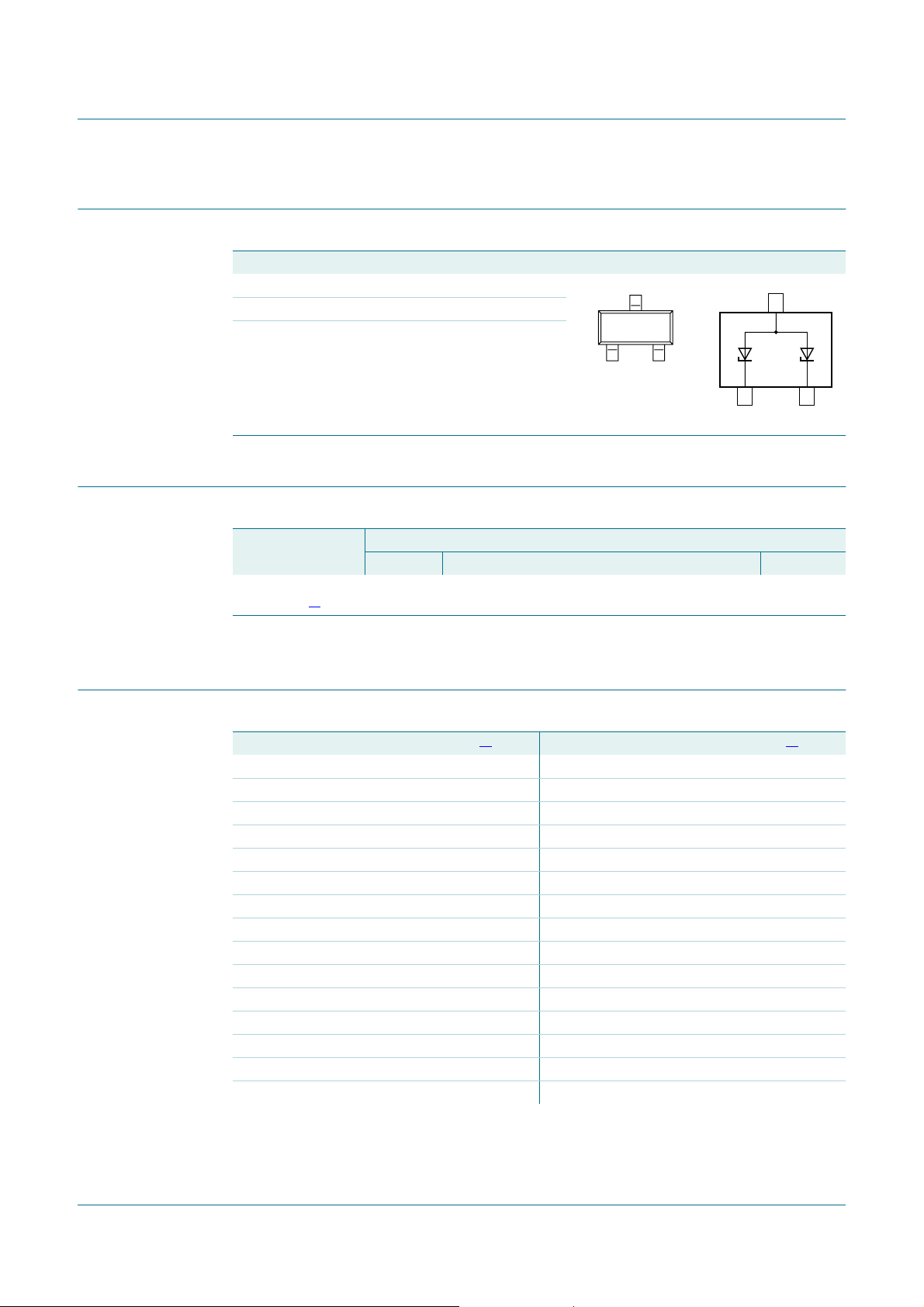
2. Pinning information
3. Ordering information
[1] The series consists of 74 types with nominal working voltages from 2.4 V to 75 V.
4. Marking
Table 2. Pinning
Pin Description Simplified outline Graphic symbol
1 cathode (diode 1)
2 cathode (diode 2)
3 common anode
12
3
006aaa154
12
3
Table 3. Ordering information
Type number Package
Name Description Version
BZB84-B2V4 to
BZB84-C75
[1]
- plastic surface-mounted package; 3 leads SOT23
Table 4. Marking codes
Type number Marking code
[1]
Type number Marking code
[1]
BZB84-B2V4 V9* BZB84-C2V4 U9*
BZB84-B2V7 VA* BZB84-C2V7 UA*
BZB84-B3V0 VB* BZB84-C3V0 UB*
BZB84-B3V3 VC* BZB84-C3V3 UC*
BZB84-B3V6 VD* BZB84-C3V6 UD*
BZB84-B3V9 VE* BZB84-C3V9 UE*
BZB84-B4V3 VF* BZB84-C4V3 UF*
BZB84-B4V7 VG* BZB84-C4V7 UG*
BZB84-B5V1 VH* BZB84-C5V1 UH*
BZB84-B5V6 VK* BZB84-C5V6 UK*
BZB84-B6V2 VL* BZB84-C6V2 UL*
BZB84-B6V8 VM* BZB84-C6V8 UM*
BZB84-B7V5 VN* BZB84-C7V5 UN*
BZB84-B8V2 VP* BZB84-C8V2 UP*
BZB84-B9V1 VR* BZB84-C9V1 UR*

BZB84_SER_3 © NXP B.V. 2009. All rights reserved.
Product data sheet Rev. 03 — 9 June 2009 3 of 14
NXP Semiconductors
BZB84 series
Dual Zener diodes
[1] * = -: made in Hong Kong
* = p: made in Hong Kong
* = t: made in Malaysia
* = W: made in China
5. Limiting values
BZB84-B10 VS* BZB84-C10 US*
BZB84-B11 VT* BZB84-C11 UT*
BZB84-B12 VU* BZB84-C12 UU*
BZB84-B13 VV* BZB84-C13 UV*
BZB84-B15 VW* BZB84-C15 UW*
BZB84-B16 PT* BZB84-C16 PB*
BZB84-B18 PU* BZB84-C18 PC*
BZB84-B20 RP* BZB84-C20 RQ*
BZB84-B22 PV* BZB84-C22 PD*
BZB84-B24 PW* BZB84-C24 PE*
BZB84-B27 PX* BZB84-C27 PF*
BZB84-B30 PY* BZB84-C30 PG*
BZB84-B33 PZ* BZB84-C33 PH*
BZB84-B36 RA* BZB84-C36 PJ*
BZB84-B39 RB* BZB84-C39 PK*
BZB84-B43 RC* BZB84-C43 PL*
BZB84-B47 RD* BZB84-C47 PM*
BZB84-B51 RE* BZB84-C51 PN*
BZB84-B56 RF* BZB84-C56 PP*
BZB84-B62 RG* BZB84-C62 PQ*
BZB84-B68 RH* BZB84-C68 PR*
BZB84-B75 RJ* BZB84-C75 PS*
Table 4. Marking codes
…continued
Type number Marking code
[1]
Type number Marking code
[1]
Table 5. Limiting values
In accordance with the Absolute Maximum Rating System (IEC 60134).
Symbol Parameter Conditions Min Max Unit
Per diode
I
F
forward current - 200 mA
I
ZSM
non-repetitive peak
reverse current
[1]
- see
Table 8, 9,
10 and 11
P
ZSM
non-repetitive peak
reverse power dissipation
[1]
-40W

BZB84_SER_3 © NXP B.V. 2009. All rights reserved.
Product data sheet Rev. 03 — 9 June 2009 4 of 14
NXP Semiconductors
BZB84 series
Dual Zener diodes
[1] t
p
= 100 µs; square wave; T
j
=25°C prior to surge
[2] Device mounted on an FR4 Printed-Circuit Board (PCB), single-sided copper, tin-plated and standard
footprint.
6. Thermal characteristics
[1] Device mounted on an FR4 PCB, single-sided copper, tin-plated and standard footprint.
[2] Soldering points at pins 1 and 2.
7. Characteristics
[1] Pulse test: t
p
≤ 300 µs; δ≤0.02.
Per device
P
tot
total power dissipation T
amb
≤ 25 °C
[2]
- 300 mW
T
j
junction temperature - 150 °C
T
amb
ambient temperature −55 +150 °C
T
stg
storage temperature −65 +150 °C
Table 5. Limiting values
…continued
In accordance with the Absolute Maximum Rating System (IEC 60134).
Symbol Parameter Conditions Min Max Unit
Table 6. Thermal characteristics
Symbol Parameter Conditions Min Typ Max Unit
Per device; single diode loaded
R
th(j-a)
thermal resistance from
junction to ambient
in free air
[1]
- - 417 K/W
R
th(j-sp)
thermal resistance from
junction to solder point
[2]
- - 100 K/W
Table 7. Characteristics
T
j
=25
°
C unless otherwise specified.
Symbol Parameter Conditions Min Typ Max Unit
Per diode
V
F
forward voltage I
F
=10mA
[1]
- - 0.9 V

BZB84_SER_3 © NXP B.V. 2009. All rights reserved.
Product data sheet Rev. 03 — 9 June 2009 5 of 14
NXP Semiconductors
BZB84 series
Dual Zener diodes
[1] f = 1 MHz; V
R
=0V
[2] t
p
= 100 µs; square wave; T
j
=25°C prior to surge
Table 8. Characteristics per type; BZB84-B2V4 to BZB84-B24
T
j
=25
°
C unless otherwise specified.
BZB84-
Bxxx
Working voltage
V
Z
(V)
Differential
resistance
r
dif
(Ω)
Reverse current
I
R
(µA)
Temperature
coefficient
S
Z
(mV/K)
Diode
capacitance
C
d
(pF)
[1]
Non-repetitive
peak reverse
current
I
ZSM
(A)
[2]
I
Z
=5mA I
Z
=1mA I
Z
=5mA I
Z
=5mA
Min Max Max Max Max V
R
(V) Min Max Max Max
2V4 2.35 2.45 600 100 50 1 −3.5 0 450 6.0
2V7 2.65 2.75 600 100 20 1 −3.5 0 450 6.0
3V0 2.94 3.06 600 95 10 1 −3.5 0 450 6.0
3V3 3.23 3.37 600 95 5 1 −3.5 0 450 6.0
3V6 3.53 3.67 600 90 5 1 −3.5 0 450 6.0
3V9 3.82 3.98 600 90 3 1 −3.5 0 450 6.0
4V3 4.21 4.39 600 90 3 1 −3.5 0 450 6.0
4V7 4.61 4.79 500 80 3 2 −3.5 0.2 300 6.0
5V1 5.00 5.20 480 60 2 2 −2.7 1.2 300 6.0
5V6 5.49 5.71 400 40 1 2 −2.0 2.5 300 6.0
6V2 6.08 6.32 150 10 3 4 0.4 3.7 200 6.0
6V8 6.66 6.94 80 15 2 4 1.2 4.5 200 6.0
7V5 7.35 7.65 80 15 1 5 2.5 5.3 150 4.0
8V2 8.04 8.36 80 15 0.70 5 3.2 6.2 150 4.0
9V1 8.92 9.28 100 15 0.50 6 3.8 7.0 150 3.0
10 9.80 10.20 150 20 0.20 7 4.5 8.0 90 3.0
11 10.80 11.20 150 20 0.10 8 5.4 9.0 85 2.5
12 11.80 12.20 150 25 0.10 8 6.0 10.0 85 2.5
13 12.70 13.30 170 30 0.10 8 7.0 11.0 80 2.5
15 14.70 15.30 200 30 0.05 10.5 9.2 13.0 75 2.0
16 15.70 16.30 200 40 0.05 11.2 10.4 14.0 75 1.5
18 17.60 18.40 225 45 0.05 12.6 12.4 16.0 70 1.5
20 19.6 20.4 225 55 0.05 14.0 14.4 18.0 60 1.5
22 21.6 22.4 250 55 0.05 15.4 16.4 20.0 60 1.25
24 23.5 24.5 250 70 0.05 16.8 18.4 22.0 55 1.25
Loading...