


PDTC143TE
Table of contents
 Loading...
NXP PDTC143TE, PDTC143TEF, PDTC143TK, PDTC143TM, PDTC143TS Schematic [ru]
...
DATA SH EET
Product data sheet
Supersedes data of 2004 Apr 06
2004 Aug 06
DISCRETE SEMICONDUCTORS
PDTC143T series
NPN resistor-equipped transistors;
R1 = 4.7 kΩ, R2 = open
2004 Aug 06 2
NXP Semiconductors Product data sheet
NPN resistor-equipped transistors;
R1 = 4.7 kΩ, R2 = open
PDTC143T series
FEATURES
• Built-in bias resistors
• Simplified circuit design
• Reduction of component count
• Reduced pick and place costs.
APPLICATIONS
• General purpose switching and amplification
• Inverter and interface circuits
• Circuit applications.
QUICK REFERENCE DATA
DESCRIPTION
NPN resistor-equipped transistor (see “Simplified outline,
symbol and pinning” for package details).
SYMBOL PARAMETER TYP. MAX. UNIT
V
CEO
collector-emitter
voltage
− 50 V
I
O
output current (DC) − 100 mA
R1 bias resistor 4.7 − kΩ
R2 open − − −
PRODUCT OVERVIEW
Note
1. * = p: Made in Hong Kong.
* = t: Made in Malaysia.
* = W: Made in China.
T YPE NUMBER
PACKAGE
MARKING CODE PNP COMPLEMENT
PHILIPS EIAJ
PDTC143TE SOT416 SC-75 40 PDTA143TE
PDTC143TEF SOT490 SC-89 11 PDTA143TEF
PDTC143TK SOT346 SC-59 52 PDTA143TK
PDTC143TM SOT883 SC-101 DM PDTA143TM
PDTC143TS SOT54 (TO-92) SC-43 TC143T PDTA143TS
PDTC143TT SOT23 − *33
(1)
PDTA143TT
PDTC143TU SOT323 SC-70 *52
(1)
PDTA143TU
2004 Aug 06 3
NXP Semiconductors Product data sheet
NPN resistor-equipped transistors;
R1 = 4.7 kΩ, R2 = open
PDTC143T series
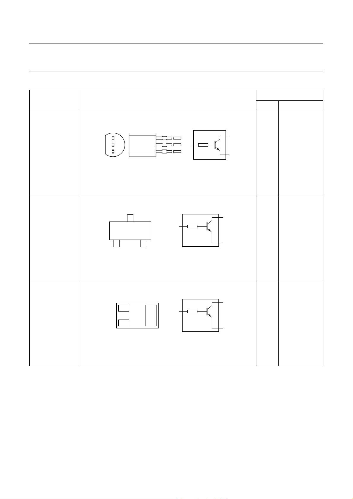
SIMPLIFIED OUTLINE, SYMBOL AND PINNING
T YPE NUMBER SIMPLIFIED OUTLINE AND SYMBOL
PINNING
PIN DESCRIPTION
PDTC143TS 1 base
2 collector
3 emitter
PDTC143TE 1 base
PDTC143TEF 2 emitter
PDTC143TK 3 collector
PDTC143TT
PDTC143TU
PDTC143TM 1 base
2 emitter
3 collector
handbook, halfpage
MAM361
1
2
3
2
3
1
R1
handbook, halfpage
MDB270
1
2
3
Top view
R1
1
2
3
handbook, halfpage
MHC507
1
2
3
R1
2
1
3
Bottom view

2004 Aug 06 4
NXP Semiconductors Product data sheet
NPN resistor-equipped transistors;
R1 = 4.7 kΩ, R2 = open
PDTC143T series
ORDERING INFORMATION
LIMITING VALUES
In accordance with the Absolu te Maximum Rating System (IEC 60134).
Notes
1. Refer to standard mounting conditions.
2. Reflow soldering is the only recommended soldering method.
3. Refer to SOT883 standard mounting conditions; FR4 with 60 μm copper strip line.
TYPE NUMBER
PACKAGE
NAME DESCRIPTION VERSION
PDTC143TE − plastic surface mounted package; 3 leads SOT416
PDTC143TEF − plastic surface mounted package; 3 leads SOT490
PDTC143TK − plastic surface mounted package; 3 leads SOT346
PDTC143TM − leadless ultra small plastic package; 3 solder lands; body
1.0
× 0.6 × 0.5 mm
SOT883
PDTC143TS − plastic single-ended leaded (through hole) package; 3 leads SOT54
PDTC143TT − plastic surface mounted package; 3 leads SOT23
PDTC143TU − plastic surface mounted package; 3 leads SOT323
SYMBOL PARAMETER CONDITIONS MIN. MAX. UNIT
V
CBO
collector-base voltage open emitter − 50 V
V
CEO
collector-emitter voltage open base − 50 V
V
EBO
emitter-base voltage open collector − 5 V
I
O
output current (DC) − 100 mA
I
CM
collector current − 100 mA
P
tot
total power dissipation T
amb
≤ 25 °C
SOT54 note 1 − 500 mW
SOT23 note 1 − 250 mW
SOT346 note 1 − 250 mW
SOT323 note 1 − 200 mW
SOT490 notes 1 and 2 − 250 mW
SOT883 notes 2 and 3 − 250 mW
SOT416 note 1 − 150 mW
T
stg
storage temperature −65 +150 °C
T
j
junction temperature − 150 °C
T
amb
operating ambient
temperature
−65 +150 °C

2004 Aug 06 5
NXP Semiconductors Product data sheet
NPN resistor-equipped transistors;
R1 = 4.7 kΩ, R2 = open
PDTC143T series
THERMAL CHARACTERISTICS
Notes
1. Refer to standard mounting conditions.
2. Reflow soldering is the only recommended soldering method.
3. Refer to SOT883 standard mounting conditions; FR4 with 60 μm copper strip line.
CHARACTERISTICS
T
amb
= 25 °C unless otherwise specified.
SYMBOL PARAMETER CONDITIONS VALUE UNIT
R
th(j-a)
thermal resistance from junction to ambient in free air
SOT54 note 1 250 K/W
SOT23 note 1 500 K/W
SOT346 note 1 500 K/W
SOT323 note 1 625 K/W
SOT490 notes 1 and 2 500 K/W
SOT883 notes 2 and 3 500 K/W
SOT416 note 1 833 K/W
SYMBOL PARAMETER CONDITIONS MIN. TYP. MAX. UNIT
I
CBO
collector-base cut-off curren t V
CB
= 50 V; I
E
= 0 A − − 100 nA
I
CEO
collector-emitter cut-off current V
CE
= 30 V; I
B
= 0 A − − 1 μA
V
CE
= 30 V; I
B
= 0 A; T
j
= 150 °C − − 50 μA
I
EBO
emitter-base cut-off current V
EB
= 5 V; I
C
= 0 A − − 100 nA
h
FE
DC current gain V
CE
= 5 V; I
C
= 1 mA 200 − −
V
CEsat
collector-emitter saturation voltage I
C
= 5 mA; I
B
= 0.25 mA − − 100 mV
R1 input resistor 3.3 4.7 6.1 kΩ
C
c
collector capacitance I
E
= i
e
= 0 A; V
CB
= 10 V;
f
= 1 MHz
− − 2.5 pF
Loading...