


 Loading...
NXP 74LVC2G126DC, 74LVC2G126DP, 74LVC2G126GD, 74LVC2G126GF, 74LVC2G126GM Schematic [ru]
...74LVC2G126
Dual bus buffer/line driver; 3-state
Rev. 12 — 8 April 2013 Product data sheet
1. General description
The 74LVC2G126 is a dual non-inverting buffer/line driver with 3-state outputs. Each 3-state output is controlled by an output enable input (pin nOE). A LOW-level at pin nOE causes the output to assume a high-impedance OFF-state. Schmitt trigger action at all inputs makes the circuit highly tolerant of slower input rise and fall times.
Inputs can be driven from either 3.3 V or 5 V devices. This feature allows the use of the 74LVC2G126 as a translator in a mixed 3.3 V and 5 V environment.
It is fully specified for partial power-down applications using IOFF. The IOFF circuitry disables the output, preventing a damaging backflow current through the device when it is powered down.
2.Features and benefits
Wide supply voltage range from 1.65 V to 5.5 V
5 V tolerant input/output for interfacing with 5 V logic
High noise immunity
Complies with JEDEC standard:
JESD8-7 (1.65 V to 1.95 V)
JESD8-5 (2.3 V to 2.7 V)
JESD8-B/JESD36 (2.7 V to 3.6 V)
ESD protection:
HBM JESD22-A114F exceeds 2000 V
MM JESD22-A115-A exceeds 200 V
24 mA output drive (VCC = 3.0 V)
CMOS low power consumption
Latch-up performance exceeds 250 mA
Direct interface with TTL levels
Inputs accept voltages up to 5 V
Multiple package options
Specified from 40 C to +85 C and 40 C to +125 C

NXP Semiconductors |
|
74LVC2G126 |
||||
|
|
|
|
|
Dual bus buffer/line driver; 3-state |
|
3. |
Ordering information |
|
|
|
||
Table 1. |
Ordering information |
|
|
|
||
|
|
|
|
|
||
Type number |
Package |
|
|
|
||
|
|
|
|
|
|
|
|
|
|
Temperature range |
Name |
Description |
Version |
74LVC2G126DP |
40 C to +125 C |
TSSOP8 |
plastic thin shrink small outline package; 8 leads; |
SOT505-2 |
||
|
|
|
|
|
body width 3 mm; lead length 0.5 mm |
|
|
|
|
|
|
||
74LVC2G126DC |
40 C to +125 C |
VSSOP8 |
plastic very thin shrink small outline package; 8 leads; |
SOT765-1 |
||
|
|
|
|
|
body width 2.3 mm |
|
|
|
|
|
|
||
74LVC2G126GT |
40 C to +125 C |
XSON8 |
plastic extremely thin small outline package; no leads; |
SOT833-1 |
||
|
|
|
|
|
8 terminals; body 1 1.95 0.5 mm |
|
|
|
|
|
|
||
74LVC2G126GF |
40 C to +125 C |
XSON8 |
extremely thin small outline package; no leads; |
SOT1089 |
||
|
|
|
|
|
8 terminals; body 1.35 1 0.5 mm |
|
|
|
|
|
|
||
74LVC2G126GD |
40 C to +125 C |
XSON8 |
plastic extremely thin small outline package; no leads; |
SOT996-2 |
||
|
|
|
|
|
8 terminals; body 3 2 0.5 mm |
|
|
|
|
|
|
||
74LVC2G126GM |
40 C to +125 C |
XQFN8 |
plastic, extremely thin quad flat package; no leads; |
SOT902-2 |
||
|
|
|
|
|
8 terminals; body 1.6 1.6 0.5 mm |
|
|
|
|
|
|
||
74LVC2G126GN |
40 C to +125 C |
XSON8 |
extremely thin small outline package; no leads; |
SOT1116 |
||
|
|
|
|
|
8 terminals; body 1.2 1.0 0.35 mm |
|
|
|
|
|
|
||
74LVC2G126GS |
40 C to +125 C |
XSON8 |
extremely thin small outline package; no leads; |
SOT1203 |
||
|
|
|
|
|
8 terminals; body 1.35 1.0 0.35 mm |
|
|
|
|
|
|
|
|
4. |
Marking |
|
|
|
|
|
Table 2. |
Marking codes |
|
|
|
||
|
|
|
|
|
||
Type number |
|
|
Marking code[1] |
|
||
74LVC2G126DP |
|
|
V26 |
|
||
|
|
|
|
|
||
74LVC2G126DC |
|
|
V26 |
|
||
|
|
|
|
|
||
74LVC2G126GT |
|
|
V26 |
|
||
|
|
|
|
|
||
74LVC2G126GF |
|
|
VN |
|
||
|
|
|
|
|
||
74LVC2G126GD |
|
|
V26 |
|
||
|
|
|
|
|
||
74LVC2G126GM |
|
|
V26 |
|
||
|
|
|
|
|
||
74LVC2G126GN |
|
|
VN |
|
||
|
|
|
|
|
||
74LVC2G126GS |
|
|
VN |
|
||
|
|
|
|
|
|
|
[1]The pin 1 indicator is located on the lower left corner of the device, below the marking code.
74LVC2G126 |
All information provided in this document is subject to legal disclaimers. |
© NXP B.V. 2013. All rights reserved. |
Product data sheet |
Rev. 12 — 8 April 2013 |
2 of 22 |

NXP Semiconductors |
74LVC2G126 |
|
Dual bus buffer/line driver; 3-state |
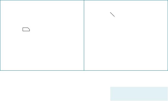
5. Functional diagram
1A |
1Y |
|
|
1OE |
|
|
|
2A |
2Y |
nA |
nY |
2OE |
|
|
|
|
001aah787 |
nOE |
mna234 |
|
|
||
Fig 1. Logic symbol |
|
Fig 2. Logic diagram (one gate) |
|
6.Pinning information
6.1Pinning
|
|
|
|
|
|
74LVC2G126 |
|
|||
|
|
|
|
|
|
|
|
|
|
|
|
|
|
|
|
|
|
|
|
|
|
|
|
|
|
1OE |
1 |
|
8 |
|
VCC |
|
|
|
|
|
|
|
|
|
|
|
|
|
74LVC2G126 |
|
|
1A |
|
2 |
|
7 |
|
2OE |
|
|
|
|
|
|
|
|
|
|
|
|
|
|
|
|
|
|
|
|
|
|
|
|
|
|
|
|
|
|
|
|
|
1OE |
1 |
8 |
VCC |
2Y |
|
3 |
|
6 |
|
1Y |
|
|
|
|
|
|
|
||||
|
|
|
|
|
|
|
||||
1A |
2 |
7 |
2OE |
|
|
|
|
|
|
|
|
|
|
|
|
|
|
|
|
|
2A |
2Y |
3 |
6 |
1Y |
GND |
|
4 |
|
5 |
|
|
GND |
4 |
5 |
2A |
|
|
|
|
|
|
|
|
|
|
|
001aab741 |
||||||
|
|
|
|
|
|
|
|
|||
|
001aab740 |
|
|
Transparent top view |
||||||
Fig 3. Pin configuration SOT505-2 and SOT765-1 |
Fig 4. Pin configuration SOT833-1, SOT1089, |
|||||||||
|
|
|
|
SOT1116 and SOT1203 |
|
|||||
|
|
|
|
|
|
|
|
|
|
|
74LVC2G126 |
All information provided in this document is subject to legal disclaimers. |
© NXP B.V. 2013. All rights reserved. |
Product data sheet |
Rev. 12 — 8 April 2013 |
3 of 22 |
NXP Semiconductors |
74LVC2G126 |
|
Dual bus buffer/line driver; 3-state |
|
|
|
|
|
|
1OE |
1 |
|
8 |
VCC |
|
|
|
|
|
|
|
1A |
|
2 |
|
7 |
2OE |
|
|
|
74LVC2G126 |
|
|
2Y |
|
3 |
|
6 |
1Y |
|
|
|
|
|
|
GND |
|
4 |
|
5 |
2A |
|
|
|
|
|
|
|
|
|
001aah949 |
||
|
|
|
Transparent top view |
|
|
Fig 5. Pin configuration SOT996-2
|
|
|
|
74LVC2G126 |
|
|
|
||||
terminal 1 |
|
|
|
|
|
CC |
|
|
|
||
index area |
|
|
|
|
|
|
|
|
|||
|
|
|
|
|
V |
|
|
|
|||
|
|
|
|
|
|
|
|
|
|
|
|
|
|
|
|
|
|
|
|
|
|
|
|
2OE |
|
1 |
|
|
|
8 |
|
|
|
|
|
|
|
|
|
|
|
|
7 |
|
1OE |
||
|
|
|
|
|
|
|
|
|
|
||
|
|
|
|
|
|
|
|
|
|
|
|
|
|
|
|
|
|
|
|
|
|
|
|
|
|
|
|
|
|
|
|
|
|
|
|
1Y |
|
2 |
|
|
|
|
|
|
6 |
|
1A |
|
|
|
|
|
|
|
|
|
|
|
|
|
|
|
|
|
|
|
|
|
|
|
|
|
|
|
|
|
|
|
|
|
|
|
|
2A |
|
3 |
|
|
|
4 |
|
|
5 |
|
2Y |
|
|
|
|
|
|
|
|
|
|
||
|
|
|
|
|
|
|
|
|
|
|
|
|
|
|
|
|
|
|
|
|
|
|
|
|
|
|
|
|
|
GND |
001aaf056 |
||||
|
|
|
|
|
|
|
|
|
|||
Transparent top view
Fig 6. Pin configuration SOT902-2
6.2 Pin description
Table 3. |
Pin description |
|
|
|
||
|
|
|
|
|
|
|
Symbol |
|
Pin |
|
Description |
||
|
|
SOT505-2, SOT765-1, SOT833-1, SOT1089, |
SOT902-2 |
|
|
|
|
|
SOT996-2, SOT1116 and SOT1203 |
|
|
|
|
1OE, 2OE |
1, 7 |
|
7, 1 |
output enable input (active HIGH) |
||
|
|
|
|
|
|
|
1A, 2A |
2, 5 |
|
6, 3 |
data input |
||
|
|
|
|
|
|
|
1Y, 2Y |
6, 3 |
|
2, 5 |
data output |
||
|
|
|
|
|
|
|
GND |
4 |
|
4 |
ground (0 V) |
||
|
|
|
|
|
|
|
VCC |
8 |
|
8 |
supply voltage |
||
|
|
|
|
|
||
7. Functional description |
|
|
|
|||
Table 4. |
Function table[1] |
|
|
|
||
Input |
|
|
|
|
|
Output |
nOE |
|
|
nA |
|
|
nY |
H |
|
|
L |
|
|
L |
|
|
|
|
|
|
|
H |
|
|
H |
|
|
H |
|
|
|
|
|
|
|
L |
|
|
X |
|
|
Z |
|
|
|
|
|
|
|
[1]H = HIGH voltage level; L = LOW voltage level; X = don’t care; Z = high-impedance OFF-state.
74LVC2G126 |
All information provided in this document is subject to legal disclaimers. |
© NXP B.V. 2013. All rights reserved. |
Product data sheet |
Rev. 12 — 8 April 2013 |
4 of 22 |

NXP Semiconductors |
74LVC2G126 |
|
Dual bus buffer/line driver; 3-state |
8. Limiting values
Table 5. Limiting values
In accordance with the Absolute Maximum Rating System (IEC 60134). Voltages are referenced to GND (ground = 0 V).
Symbol |
Parameter |
Conditions |
|
Min |
Max |
Unit |
VCC |
supply voltage |
|
|
0.5 |
+6.5 |
V |
IIK |
input clamping current |
VI < 0 V |
|
50 |
- |
mA |
VI |
input voltage |
|
[1] |
0.5 |
+6.5 |
V |
IOK |
output clamping current |
VO > VCC or VO < 0 V |
|
- |
50 |
mA |
VO |
output voltage |
Active mode |
[1] |
0.5 |
VCC + 0.5 |
V |
|
|
Power-down mode |
[1][2] |
0.5 |
+6.5 |
V |
|
|
|
|
|
|
|
IO |
output current |
VO = 0 V to VCC |
|
- |
50 |
mA |
ICC |
supply current |
|
|
- |
+100 |
mA |
IGND |
ground current |
|
|
100 |
- |
mA |
Ptot |
total power dissipation |
Tamb = 40 C to +125 C |
[3] |
- |
300 |
mW |
Tstg |
storage temperature |
|
|
65 |
+150 |
C |
[1]The input and output voltage ratings may be exceeded if the input and output current ratings are observed.
[2]When VCC = 0 V (Power-down mode), the output voltage can be 5.5 V in normal operation.
[3]For TSSOP8 packages: above 55 C the value of Ptot derates linearly at 2.5 mW/K. For VSSOP8 packages: above 110 C the value of Ptot derates linearly at 8.0 mW/K.
For XSON8 and XQFN8 packages: above 118 C the value of Ptot derates linearly with 7.8 mW/K.
9. Recommended operating conditions
Table 6. |
Operating conditions |
|
|
|
|
|
|
|
|
|
|
Symbol |
Parameter |
Conditions |
Min |
Max |
Unit |
VCC |
supply voltage |
|
1.65 |
5.5 |
V |
VI |
input voltage |
|
0 |
5.5 |
V |
VO |
output voltage |
Active mode |
0 |
VCC |
V |
|
|
VCC = 0 V; Power-down mode |
0 |
5.5 |
V |
Tamb |
ambient temperature |
|
40 |
+125 |
C |
t/ V |
input transition rise and fall rate |
VCC = 1.65 V to 2.7 V |
- |
20 |
ns/V |
|
|
VCC = 2.7 V to 5.5 V |
- |
10 |
ns/V |
74LVC2G126 |
All information provided in this document is subject to legal disclaimers. |
© NXP B.V. 2013. All rights reserved. |
Product data sheet |
Rev. 12 — 8 April 2013 |
5 of 22 |
NXP Semiconductors |
|
|
74LVC2G126 |
|||
|
|
|
Dual bus buffer/line driver; 3-state |
|||
10. Static characteristics |
|
|
|
|
||
Table 7. |
Static characteristics |
|
|
|
|
|
At recommended operating conditions; voltages are referenced to GND (ground = 0 V). |
|
|
|
|||
|
|
|
|
|
|
|
Symbol |
Parameter |
Conditions |
Min |
Typ[1] |
Max |
Unit |
Tamb = 40 C to +85 C |
|
|
|
|
|
|
VIH |
HIGH-level input voltage |
VCC = 1.65 V to 1.95 V |
0.65 VCC |
- |
- |
V |
|
|
VCC = 2.3 V to 2.7 V |
1.7 |
- |
- |
V |
|
|
VCC = 2.7 V to 3.6 V |
2.0 |
- |
- |
V |
|
|
VCC = 4.5 V to 5.5 V |
0.7 VCC |
- |
- |
V |
VIL |
LOW-level input voltage |
VCC = 1.65 V to 1.95 V |
- |
- |
0.35 VCC |
V |
|
|
VCC = 2.3 V to 2.7 V |
- |
- |
0.7 |
V |
|
|
VCC = 2.7 V to 3.6 V |
- |
- |
0.8 |
V |
|
|
VCC = 4.5 V to 5.5 V |
- |
- |
0.3 VCC |
V |
VOL |
LOW-level output voltage |
VI = VIH or VIL |
|
|
|
|
|
|
IO = 100 A; VCC = 1.65 V to 5.5 V |
- |
- |
0.1 |
V |
|
|
IO = 4 mA; VCC = 1.65 V |
- |
- |
0.45 |
V |
|
|
IO = 8 mA; VCC = 2.3 V |
- |
- |
0.3 |
V |
|
|
IO = 12 mA; VCC = 2.7 V |
- |
- |
0.4 |
V |
|
|
IO = 24 mA; VCC = 3.0 V |
- |
- |
0.55 |
V |
|
|
IO = 32 mA; VCC = 4.5 V |
- |
- |
0.55 |
V |
VOH |
HIGH-level output voltage |
VI = VIH or VIL |
|
|
|
|
|
|
IO = 100 A; VCC = 1.65 V to 5.5 V |
VCC 0.1 |
- |
- |
V |
|
|
IO = 4 mA; VCC = 1.65 V |
1.2 |
- |
- |
V |
|
|
IO = 8 mA; VCC = 2.3 V |
1.9 |
- |
- |
V |
|
|
IO = 12 mA; VCC = 2.7 V |
2.2 |
- |
- |
V |
|
|
IO = 24 mA; VCC = 3.0 V |
2.3 |
- |
- |
V |
|
|
IO = 32 mA; VCC = 4.5 V |
3.8 |
- |
- |
V |
II |
input leakage current |
VI = 5.5 V or GND; VCC = 0 V to 5.5 V |
- |
0.1 |
5 |
A |
IOZ |
OFF-state output current |
VI = VIH or VIL; VO = 5.5 V or GND; |
- |
0.1 |
10 |
A |
|
|
VCC = 3.6 V |
|
|
|
|
IOFF |
power-off leakage current |
VI or VO = 5.5 V; VCC = 0 V |
- |
0.1 |
10 |
A |
ICC |
supply current |
VI = 5.5 V or GND; |
- |
0.1 |
10 |
A |
|
|
VCC = 1.65 V to 5.5 V; IO = 0 A |
|
|
|
|
ICC |
additional supply current |
per pin; VI = VCC 0.6 V; IO = 0 A; |
- |
5 |
500 |
A |
|
|
VCC = 2.3 V to 5.5 V |
|
|
|
|
CI |
input capacitance |
|
- |
2 |
- |
pF |
74LVC2G126 |
All information provided in this document is subject to legal disclaimers. |
© NXP B.V. 2013. All rights reserved. |
Product data sheet |
Rev. 12 — 8 April 2013 |
6 of 22 |
NXP Semiconductors |
|
|
74LVC2G126 |
|||
|
|
|
Dual bus buffer/line driver; 3-state |
|||
Table 7. |
Static characteristics …continued |
|
|
|
|
|
At recommended operating conditions; voltages are referenced to GND (ground = 0 V). |
|
|
|
|||
|
|
|
|
|
|
|
Symbol |
Parameter |
Conditions |
Min |
Typ[1] |
Max |
Unit |
Tamb = 40 C to +125 C |
|
|
|
|
|
|
VIH |
HIGH-level input voltage |
VCC = 1.65 V to 1.95 V |
0.65 VCC |
- |
- |
V |
|
|
VCC = 2.3 V to 2.7 V |
1.7 |
- |
- |
V |
|
|
VCC = 2.7 V to 3.6 V |
2.0 |
- |
- |
V |
|
|
VCC = 4.5 V to 5.5 V |
0.7 VCC |
- |
- |
V |
VIL |
LOW-level input voltage |
VCC = 1.65 V to 1.95 V |
- |
- |
0.35 VCC |
V |
|
|
VCC = 2.3 V to 2.7 V |
- |
- |
0.7 |
V |
|
|
VCC = 2.7 V to 3.6 V |
- |
- |
0.8 |
V |
|
|
VCC = 4.5 V to 5.5 V |
- |
- |
0.3 VCC |
V |
VOL |
LOW-level output voltage |
VI = VIH or VIL |
|
|
|
|
|
|
IO = 100 A; VCC = 1.65 V to 5.5 V |
- |
- |
0.1 |
V |
|
|
IO = 4 mA; VCC = 1.65 V |
- |
- |
0.70 |
V |
|
|
IO = 8 mA; VCC = 2.3 V |
- |
- |
0.45 |
V |
|
|
IO = 12 mA; VCC = 2.7 V |
- |
- |
0.60 |
V |
|
|
IO = 24 mA; VCC = 3.0 V |
- |
- |
0.80 |
V |
|
|
IO = 32 mA; VCC = 4.5 V |
- |
- |
0.80 |
V |
VOH |
HIGH-level output voltage |
VI = VIH or VIL |
|
|
|
|
|
|
IO = 100 A; VCC = 1.65 V to 5.5 V |
VCC 0.1 |
- |
- |
V |
|
|
IO = 4 mA; VCC = 1.65 V |
0.95 |
- |
- |
V |
|
|
IO = 8 mA; VCC = 2.3 V |
1.7 |
- |
- |
V |
|
|
IO = 12 mA; VCC = 2.7 V |
1.9 |
- |
- |
V |
|
|
IO = 24 mA; VCC = 3.0 V |
2.0 |
- |
- |
V |
|
|
IO = 32 mA; VCC = 4.5 V |
3.4 |
- |
- |
V |
II |
input leakage current |
VI = 5.5 V or GND; VCC = 0 V to 5.5 V |
- |
- |
20 |
A |
IOZ |
OFF-state output current |
VI = VIH or VIL; VO = 5.5 V or GND; |
- |
- |
20 |
A |
|
|
VCC = 3.6 V |
|
|
|
|
IOFF |
power-off leakage current |
VI or VO = 5.5 V; VCC = 0 V |
- |
- |
20 |
A |
ICC |
supply current |
VI = 5.5 V or GND; |
- |
- |
40 |
A |
|
|
VCC = 1.65 V to 5.5 V; IO = 0 A |
|
|
|
|
ICC |
additional supply current |
per pin; VI = VCC 0.6 V; IO = 0 A; |
- |
- |
5 |
mA |
|
|
VCC = 2.3 V to 5.5 V |
|
|
|
|
[1]Typical values are measured at VCC = 3.3 V and Tamb = 25 C.
74LVC2G126 |
All information provided in this document is subject to legal disclaimers. |
© NXP B.V. 2013. All rights reserved. |
Product data sheet |
Rev. 12 — 8 April 2013 |
7 of 22 |
Loading...