


BFG540
Table of contents
 Loading...
BFG540; BFG540/X; BFG540/XR
NPN 9 GHz wideband transistor
Rev. 05 — 21 November 2007 Product data sheet
IMPORTANT NOTICE
Dear customer,
As from October 1st, 2006 Philips Semiconductors has a new trade name
- NXP Semiconductors, which will be used in future data sheets together with new contact
details.
In data sheets where the previous Philips references remain, please use the new links as
shown below.
http://www.philips.semiconductors.com use http://www.nxp.com
http://www.semiconductors.philips.com use http://www.nxp.com (Internet)
sales.addresses@www.semiconductors.philips.com use salesaddresses@nxp.com
(email)
The copyright notice at the bottom of each page (or elsewhere in the document,
depending on the version)
- © Koninklijke Philips Electronics N.V. (year). All rights reserved is replaced with:
- © NXP B.V. (year). All rights reserved. If you have any questions related to the data sheet, please contact our nearest sales
office via e-mail or phone (details via salesaddresses@nxp.com). Thank you for your
cooperation and understanding,
NXP Semiconductors

NXP Semiconductors Product specification
Rev. 05 - 21 November 2007
2 of 14
NPN 9 GHz wideband transistor
FEATURES
• High power gain
• Low noise figure
• High transition frequency
• Gold metallization ensures
excellent reliability.
DESCRIPTION
NPN silicon planar epitaxial
transistors, intended for wideband
applications in the GHz range, such
as analog and digital cellular
telephones, cordless telephones
(CT1, CT2, DECT, etc.), radar
detectors, satelliteTV tuners (SATV),
MATV/CATV amplifiers and repeater
amplifiers in fibre-optical systems.
Thetransistors are mountedin plastic
SOT143B and SOT143R packages.
PINNING
PIN DESCRIPTION
BFG540 (Fig.1) Code: %MG
1 collector
2 base
3 emitter
4 emitter
BFG540/X (Fig.1) Code: %MM
1 collector
2 emitter
3 base
4 emitter
BFG540/XR (Fig.2) Code: %MR
1 collector
2 emitter
3 base
4 emitter
BFG540; BFG540/X;
BFG540/XR
handbook, 2 columns
12
Top view
Fig.1 SOT143B.
handbook, 2 columns
Top view
Fig.2 SOT143R.
34
MSB014
43
12
MSB035
NXP Semiconductors Product specification
Rev. 05 - 21 November 2007
3 of 14
NPN 9 GHz wideband transistor
BFG540; BFG540/X;
BFG540/XR
QUICK REFERENCE DATA
SYMBOL PARAMETER CONDITIONS MIN. TYP. MAX. UNIT
V
CBO
V
CES
I
C
P
tot
h
FE
C
re
f
T
G
UM
2
s
21
F noise figure Γ
collector-base voltage open emitter −−20 V
collector-emitter voltage RBE=0 −−15 V
DC collector current −−120 mA
total power dissipation Ts≤ 60 °C; note 1 −−400 mW
DC current gain IC= 40 mA; VCE=8V; Tj=25°C 100 120 250
feedback capacitance IC= 0; VCE= 8 V; f = 1 MHz − 0.5 − pF
transition frequency IC= 40 mA; VCE= 8 V; f = 1 GHz;
T
=25°C
amb
maximum unilateral power gain IC= 40 mA; VCE= 8 V; f = 900 MHz;
T
=25°C
amb
I
= 40 mA; VCE= 8 V; f = 2 GHz;
C
T
=25°C
amb
insertion power gain I
= 40 mA; VCE= 8 V; f = 900 MHz;
C
T
=25°C
amb
= Γ
; IC= 10 mA; VCE=8V;
s
opt
f = 900 MHz; T
Γ
= Γ
; IC= 40 mA; VCE=8V;
s
opt
f = 900 MHz; T
= Γ
Γ
; IC= 10 mA; VCE=8V;
s
opt
f = 2 GHz; T
amb
=25°C
amb
=25°C
amb
=25°C
− 9 − GHz
− 18 − dB
− 11 − dB
15 16 − dB
− 1.3 1.8 dB
− 1.9 2.4 dB
− 2.1 − dB
LIMITING VALUES
In accordance with the Absolute Maximum System (IEC 60134).
SYMBOL PARAMETER CONDITIONS MIN. MAX. UNIT
V
V
V
I
P
T
T
CBO
CES
EBO
C
tot
stg
j
collector-base voltage open emitter − 20 V
collector-emitter voltage RBE=0 − 15 V
emitter-base voltage open collector − 2.5 V
DC collector current − 120 mA
total power dissipation Ts≤ 60 °C; note 1 − 400 mW
storage temperature −65 +150 °C
junction temperature − 150 °C
Note
1. T
is the temperature at the soldering point of the collector pin.
s
THERMAL CHARACTERISTICS
SYMBOL PARAMETER CONDITIONS VALUE UNIT
R
th j-s
thermal resistance from junction to soldering point Ts≤ 60 °C; note 1 290 K/W
Note
is the temperature at the soldering point of the collector pin.
1. T
s
NXP Semiconductors Product specification
Rev. 05 - 21 November 2007
4 of 14
NPN 9 GHz wideband transistor
BFG540; BFG540/X;
BFG540/XR
CHARACTERISTICS
Tj=25°C unless otherwise specified.
SYMBOL PARAMETER CONDITIONS MIN. TYP. MAX. UNIT
I
CBO
h
FE
C
e
C
c
C
re
f
T
G
UM
2
s
21
F noise figure Γ
P
L1
ITO third order intercept point note 2 − 34 − dBm
V
O
d
2
collector cut-off current IE= 0; VCB=8V −−50 nA
DC current gain IC= 40 mA; VCE= 8 V 60 120 250
emitter capacitance IC=ic= 0; VEB= 0.5 V; f = 1 MHz − 2 − pF
collector capacitance IE=ie= 0; VCB=8V; f=1MHz − 0.9 − pF
feedback capacitance IC= 0; VCB= 8 V; f = 1 MHz − 0.5 − pF
transition frequency IC= 40 mA; VCE= 8 V; f = 1 GHz;
T
=25°C
amb
maximum unilateral power gain
(note 1)
insertion power gain I
output power at 1 dB gain
compression
IC= 40 mA; VCE= 8 V; f = 900 MHz;
T
=25°C
amb
I
= 40 mA; VCE= 8 V; f = 2 GHz;
C
T
=25°C
amb
= 40 mA; VCE= 8 V; f = 900 MHz;
C
T
=25°C
amb
= Γ
; IC= 10 mA; VCE=8V;
s
opt
f = 900 MHz; T
Γ
= Γ
; IC= 40 mA; VCE=8V;
s
opt
f = 900 MHz; T
Γ
= Γ
; IC= 10 mA; VCE=8V;
s
opt
f = 2 GHz; T
amb
=25°C
amb
=25°C
amb
=25°C
IC= 40 mA; VCE=8V; RL=50Ω;
f = 900 MHz; T
amb
=25°C
− 9 − GHz
− 18 − dB
− 11 − dB
15 16 − dB
− 1.3 1.8 dB
− 1.9 2.4 dB
− 2.1 − dB
− 21 − dBm
output voltage note 3 − 500 − mV
second order intermodulation
note 4 −−50 − dB
distortion
Notes
1. G
2. V
is the maximum unilateral power gain, assuming s12 is zero and
UM
= 8 V; IC= 40 mA; RL=50Ω; T
CE
amb
=25°C;
fp= 900 MHz; fq= 902 MHz;
measured at f
= 898 MHz and f
(2p − q)
(2q − p)
= 904 MHz.
3. dim= −60 dB (DIN 45004B); IC= 40 mA; VCE= 8 V; ZL=ZS=75Ω; T
Vp=VO; Vq=VO−6 dB; Vr=VO−6 dB;
fp= 795.25 MHz; fq= 803.25 MHz; fr= 805.25 MHz;
measured at f
(p+q−r)
4. IC= 40 mA; VCE= 8 V; VO= 275 mV; T
fp= 250 MHz; fq= 560 MHz; measured at f
= 793.25 MHz.
amb
=25°C;
= 810 MHz.
(p + q)
G
amb
UM
=25°C;
10
-------------------------------------------------------1s
–()1s
2
s
21
2
11
–()
dB.log=
2
22
NXP Semiconductors Product specification
Rev. 05 - 21 November 2007
5 of 14
NPN 9 GHz wideband transistor
150
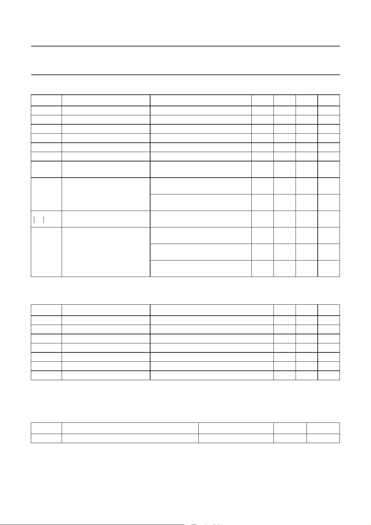
Ts(
MBG249
o
C)
600
handbook, halfpage
P
tot
(mW)
400
200
0
0 50 100 200
250
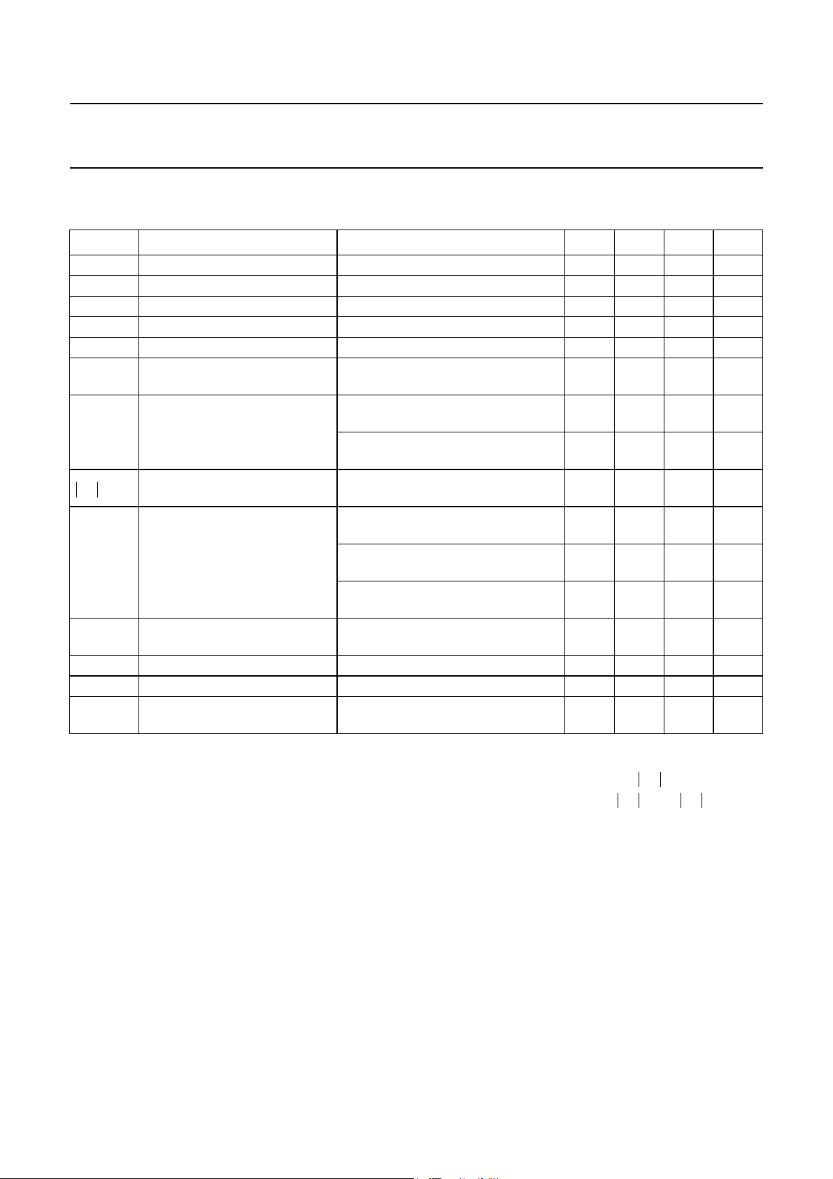
handbook, halfpage
h
FE
200
150
100
50
0
−2
10
BFG540; BFG540/X;
BFG540/XR
−1
10
11010
IC (mA)
MRA749
2
VCE≤ 10 V.
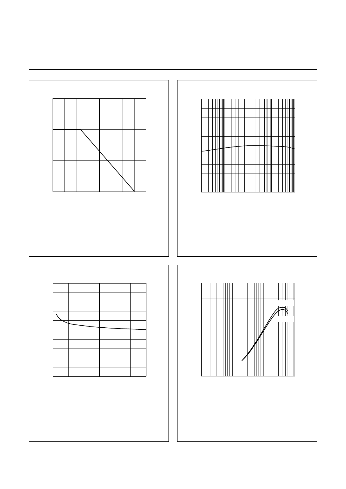
handbook, halfpage
1
C
re
(pF)
0.8
0.6
0.4
0.2
0
04
Fig.3 Power derating curve.
812
VCB (V)
MRA750
VCE= 8 V; Tj = 25 °C.
Fig.4 DC current gain as a function of collector
current.
12
handbook, halfpage
f
T
(GHz)
8
4
0
−1
10
11010
MRA751
V
= 8 V
CE
V
= 4 V
CE
IC (mA)
2
IC= 0; f = 1 MHz.
Fig.5 Feedback capacitance as a function of
collector-base voltage.
f = 1 GHz; T
amb
=25°C.
Fig.6 Transition frequency as a function of
collector current.
Loading...