


74LVC1G08GF
Table of contents
 Loading...
NXP 74LVC1G08GF, 74LVC1G08GM, 74LVC1G08GN, 74LVC1G08GS, 74LVC1G08GV Schematic [ru]
...
1. General description
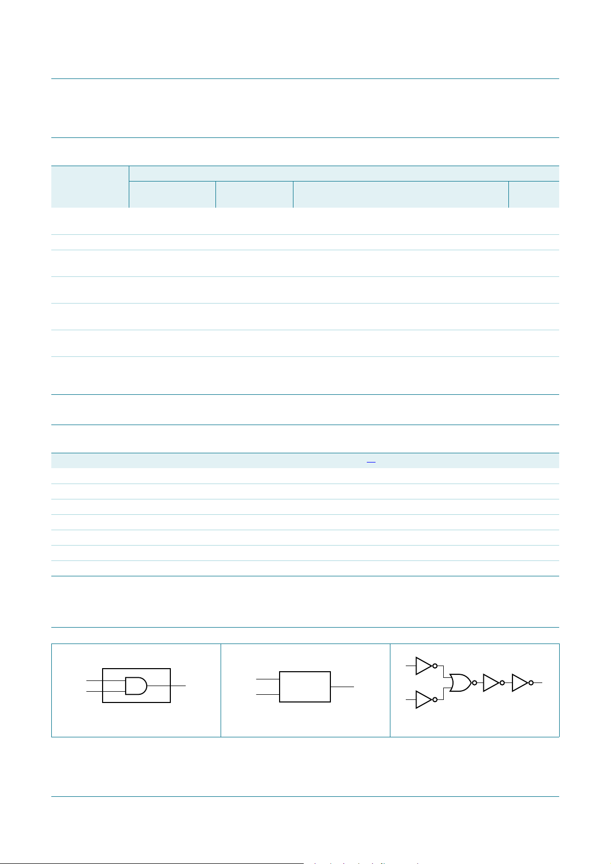
The 74LVC1G08 provides one 2-input AND function.
Inputs can be driven from either 3.3 V or 5 V devices. This feature allows the use of these
devices as translators in mixed 3.3 V and 5 V applications.
Schmitt trigger action at all inputs makes the circuit tolerant of slower input rise and fall
time.
This device is fully specified for partial power-down applications using I
OFF
.
The I
OFF
circuitry disables the output, preventing the damaging backflow current through
the device when it is powered down.
2. Features and benefits
Wide supply voltage range from 1.65 V to 5.5 V
High noise immunity
Complies with JEDEC standard:
JESD8-7 (1.65 V to 1.95 V)
JESD8-5 (2.3 V to 2.7 V)
JESD8-B/JESD36 (2.7 V to 3.6 V)
24 mA output drive (V
CC
=3.0V)
CMOS low power consumption
Latch-up performance 250 mA
Direct interface with TTL levels
Inputs accept voltages up to 5 V
ESD protection:
HBM JESD22-A114F exceeds 2000 V
MM JESD22-A115-A exceeds 200 V
Multiple package options
Specifie d from 40 C to +85 C and 40 C to +125 C
74LVC1G08
Single 2-input AND gate
Rev. 10 — 29 June 2012 Product data sheet
74LVC1G08 All information provided in this document is subject to legal disclaimers. © NXP B.V. 2012. All rights reserved.
Product data sheet Rev. 10 — 29 June 2012 2 of 19
NXP Semiconductors
74LVC1G08
Single 2-input AND gate
3. Ordering information
4. Marking
[1] The pin 1 indicator is located on the lower left corner of the device, below the marking code.
5. Functional diagram
Table 1. Ordering information
Type number Package
T emperature
range
Name Description Version
74LVC1G08GW 40 Cto+125C TSSOP5 plastic thin shrink small outline package; 5 leads;
body width 1.25 mm
SOT353-1
74LVC1G08GV 40 Cto+125C SC-74A plastic surface-mounted package; 5 leads SOT753
74LVC1G08GM 40 Cto+125C XSON6 plastic extremely thin small outline package;
no leads; 6 terminals; body 1 1.45 0.5 mm
SOT886
74LVC1G08GF 40 C to +125 C XSON6 plastic extremely thin small outline package;
no leads; 6 terminals; body 1 1 0.5 mm
SOT891
74LVC1G08GN 40 C to +125 C XSON6 extremely thin small outline package; no leads;
6 terminals; body 0.9 1.0 0.35 mm
SOT1115
74LVC1G08GS 40 C to +125 C XSON6 extremely thin small outline package; no leads;
6 terminals; body 1.0 1.0 0.35 mm
SOT1202
74LVC1G08GX 40 C to +125 C X2SON5 X2SON5: plastic thermal enhanced extremely thin
small outline package; no leads; 5 terminals;
body 0.8 0.8 0.35 mm
SOT1226
Table 2. Marking
Type number Marking code
[1]
74LVC1G08GW VE
74LVC1G08GV V08
74LVC1G08GM VE
74LVC1G08GF VE
74LVC1G08GN VE
74LVC1G08GS VE
74LVC1G08GX VE
Fig 1. Logic symbol Fig 2. IEC logic symbol Fig 3. Logic diagram
mna113
B
A
Y
2
1
4
mna114
2
4
&
1
mna221
A
B
Y

74LVC1G08 All information provided in this document is subject to legal disclaimers. © NXP B.V. 2012. All rights reserved.
Product data sheet Rev. 10 — 29 June 2012 3 of 19
NXP Semiconductors
74LVC1G08
Single 2-input AND gate
6. Pinning information
6.1 Pinning
6.2 Pin description
Fig 4. Pin configu ration SOT353-1 and SOT753 Fig 5. Pin configuration SOT886
74LVC1G08
BV
CC
A
GND Y
001aab638
1
2
3
5
4
74LVC1G08
A
001aab639
B
GND
n.c.
V
CC
Y
Transparent top view
2
3
1
5
4
6
Fig 6. Pin configu ration SOT891, SOT1115 and
SOT1202
Fig 7. Pin configuration SOT1226 (X2SON5)
74LVC1G08
A
001aae978
B
GND
n.c.
V
CC
Y
Transparent top view
2
3
1
5
4
6
B
V
CC
GND
1
3
2
5
4
A
Y
aaa-003023
Transparent top view
74LVC1G08
Table 3. Pin description
Symbol Pin Description
TSSOP5 and X2SON5 XSON6
B 1 1 data input
A 2 2 data input
GND 3 3 ground (0 V)
Y 4 4 data output
n.c. - 5 not connected
V
CC
5 6 supply voltage

74LVC1G08 All information provided in this document is subject to legal disclaimers. © NXP B.V. 2012. All rights reserved.
Product data sheet Rev. 10 — 29 June 2012 4 of 19
NXP Semiconductors
74LVC1G08
Single 2-input AND gate
7. Functional description
[1] H = HIGH voltage level; L = LOW voltage level
8. Limiting values
[1] The input and output voltage ratings may be exceeded if the input and output current ratings are observed.
[2] When V
CC
= 0 V (Power-down mode), the output voltage can be 5.5 V in normal operation.
[3] For TSSOP5 and SC-74A packages: above 87.5 C the value of P
tot
derates linearly with 4.0 mW/K.
For XSON6 and X2SON5 package: above 118 C the value of P
tot
derates linearly with 7.8 mW/K.
Table 4. Function table
[1]
Input Output
A B Y
LLL
LHL
HLL
HHH
Table 5. Limiting values
In accordance with the Absolute Maximum Rating System (IEC 60134). Voltages are referenced to GND (ground = 0 V).
Symbol Parameter Conditions Min Max Unit
V
CC
supply voltage 0.5 +6.5 V
I
IK
input clamping current V
I
< 0 V 50 - mA
V
I
input voltage
[1]
0.5 +6.5 V
I
OK
output clamping current V
O
> V
CC
or V
O
< 0 V - 50 mA
V
O
output voltage Active mode
[1][2]
0.5 V
CC
+ 0.5 V
Power-down mode
[1][2]
0.5 +6.5 V
I
O
output current V
O
= 0 V to V
CC
- 50 mA
I
CC
supply current - 100 mA
I
GND
ground current 100 - mA
P
tot
total power dissipation T
amb
= 40 C to +125 C
[3]
- 250 mW
T
stg
storage temperature 65 +150 C
74LVC1G08 All information provided in this document is subject to legal disclaimers. © NXP B.V. 2012. All rights reserved.
Product data sheet Rev. 10 — 29 June 2012 5 of 19
NXP Semiconductors
74LVC1G08
Single 2-input AND gate
9. Recommended operating conditions
10. Static characteristics
Table 6. Recommended operating conditions
Symbol Parameter Conditions Min Typ Max Unit
V
CC
supply voltage 1.65 - 5.5 V
V
I
input voltage 0 - 5.5 V
V
O
output voltage Active mode 0 - V
CC
V
V
CC
= 0 V; Power-down mode 0 - 5.5 V
T
amb
ambient temperature 40 - +125 C
t/V input transition rise and fall rate V
CC
= 1.65 V to 2.7 V - - 20 ns/V
V
CC
= 2.7 V to 5.5 V - - 10 ns/V
Table 7. Static characteristics
At recommended operating conditions. Voltages are referenced to GND (ground = 0 V).
Symbol Parameter Conditions 40 C to +85 C 40 C to +125 C Unit
Min Typ
[1]
Max Min Max
V
IH
HIGH-level
input voltage
V
CC
= 1.65 V to 1.95 V 0.65V
CC
- - 0.65V
CC
-V
V
CC
= 2.3 V to 2.7 V 1.7 - - 1.7 - V
V
CC
= 2.7 V to 3.6 V 2.0 - - 2.0 - V
V
CC
= 4.5 V to 5.5 V 0.7V
CC
- - 0.7V
CC
-V
V
IL
LOW-level
input voltage
V
CC
= 1.65 V to 1.95 V - - 0.35V
CC
-0.35V
CC
V
V
CC
= 2.3 V to 2.7 V - - 0.7 - 0.7 V
V
CC
= 2.7 V to 3.6 V - - 0.8 - 0.8 V
V
CC
= 4.5 V to 5.5 V - - 0.3V
CC
-0.3V
CC
V
V
OH
HIGH-level
output voltage
V
I
=V
IH
or V
IL
I
O
= 100 A;
V
CC
= 1.65 V to 5.5 V
V
CC
0.1 - - V
CC
0.1 - V
I
O
= 4mA; V
CC
= 1.65 V 1.2 - - 0.95 - V
I
O
= 8mA; V
CC
= 2.3 V 1.9 - - 1.7 - V
I
O
= 12 mA; V
CC
= 2.7 V 2.2 - - 1.9 - V
I
O
= 24 mA; V
CC
= 3.0 V 2.3 - - 2.0 - V
I
O
= 32 mA; V
CC
= 4.5 V 3.8 - - 3.4 - V
V
OL
LOW-level
output voltage
V
I
=V
IH
or V
IL
I
O
=100A;
V
CC
= 1.65 V to 5.5 V
- - 0.10 - 0.10 V
I
O
=4mA; V
CC
= 1.65 V - - 0.45 - 0.70 V
I
O
=8mA; V
CC
= 2.3 V - - 0.30 - 0.45 V
I
O
=12mA; V
CC
= 2.7 V - - 0.40 - 0.60 V
I
O
=24mA; V
CC
= 3.0 V - - 0.55 - 0.80 V
I
O
=32mA; V
CC
= 4.5 V - - 0.55 - 0.80 V
I
I
input leakage
current
V
I
= 5.5 V or GND;
V
CC
=0Vto5.5V
- 0.1 5-100 A
74LVC1G08 All information provided in this document is subject to legal disclaimers. © NXP B.V. 2012. All rights reserved.
Product data sheet Rev. 10 — 29 June 2012 6 of 19
NXP Semiconductors
74LVC1G08
Single 2-input AND gate
[1] All typical values are measured at V
CC
= 3.3 V and T
amb
=25C.
11. Dynamic characteristics
[1] Typical values are measured at T
amb
=25C and V
CC
= 1.8 V, 2.5 V, 2.7 V, 3.3 V and 5.0 V respectively.
[2] t
pd
is the same as t
PLZ
and t
PZL
.
[3] C
PD
is used to determine the dynamic power dissipation (P
D
in W).
P
D
=C
PD
V
CC
2
f
i
N+(C
L
V
CC
2
f
o
) where:
f
i
= input frequency in MHz;
f
o
= output frequency in MHz;
C
L
= output load capacitance in pF;
V
CC
= supply voltage in V;
N = number of inputs switching;
(C
L
V
CC
2
f
o
) = sum of outputs.
I
OFF
power-off
leakage
current
V
CC
= 0 V; V
I
or V
O
=5.5V - 0.1 10 - 200 A
I
CC
supply current V
I
= 5.5 V or GND; I
O
= 0 A;
V
CC
= 1.65 V to 5.5 V
-0.110 - 200A
I
CC
additional
supply current
per pin; V
CC
= 2.3 V to 5.5 V;
V
I
=V
CC
0.6 V; I
O
=0 A
- 5 500 - 5000 A
C
I
input
capacitance
V
CC
= 3.3 V; V
I
= GND to V
CC
-5- - -pF
Table 7. Static characteristics
…continued
At recommended operating conditions. Voltages are referenced to GND (ground = 0 V).
Symbol Parameter Conditions 40 C to +85 C 40 C to +125 C Unit
Min Typ
[1]
Max Min Max
Table 8. Dynamic characteristics
Voltages are referenced to GND (ground = 0 V); for load circuit see Figure 9.
Symbol Parameter Conditions 40 C to +85 C 40 C to +125 C Unit
Min Typ
[1]
Max Min Max
t
pd
propagation delay A, B to Y; see Figure 8
[2]
V
CC
= 1.65 V to 1.95 V 1.0 3.4 8.0 1.0 10.5 ns
V
CC
= 2.3 V to 2.7 V 0.5 2.2 5.5 0.5 7.0 ns
V
CC
= 2.7 V 0.5 2.5 5.5 0.5 7.0 ns
V
CC
= 3.0 V to 3.6 V 0.5 2.1 4.5 0.5 6.0 ns
V
CC
= 4.5 V to 5.5 V 0.5 1.7 4.0 0.5 5.5 ns
C
PD
power dissipation
capacitance
V
I
= GND to V
CC
; V
CC
= 3.3 V
[3]
-16- - -pF
Loading...