


 Loading...
LPC178x/7x
32-bit ARM Cortex-M3 microcontroller; up to 512 kB flash and 96 kB SRAM; USB Device/Host/OTG; Ethernet; LCD; EMC
Rev. 5 — 9 September 2014 |
Product data sheet |
1. General description
The LPC178x/7x is an ARM Cortex-M3 based microcontroller for embedded applications requiring a high level of integration and low power dissipation.
The ARM Cortex-M3 is a next generation core that offers better performance than the ARM7 at the same clock rate and other system enhancements such as modernized debug features and a higher level of support block integration. The ARM Cortex-M3 CPU incorporates a 3-stage pipeline and has a Harvard architecture with separate local instruction and data buses, as well as a third bus with slightly lower performance for peripherals. The ARM Cortex-M3 CPU also includes an internal prefetch unit that supports speculative branches.
The LPC178x/7x adds a specialized flash memory accelerator to accomplish optimal performance when executing code from flash. The LPC178x/7x operates at up to 120 MHz CPU frequency.
The peripheral complement of the LPC178x/7x includes up to 512 kB of flash program memory, up to 96 kB of SRAM data memory, up to 4032 byte of EEPROM data memory, External Memory Controller (EMC), LCD (LPC178x only), Ethernet, USB Device/Host/OTG, a General Purpose DMA controller, five UARTs, three SSP controllers, three I2C-bus interfaces, a Quadrature Encoder Interface, four general purpose timers, two general purpose PWMs with six outputs each and one motor control PWM, an ultra-low power RTC with separate battery supply and event recorder, a windowed watchdog timer, a CRC calculation engine, up to 165 general purpose I/O pins, and more.
The analog peripherals include one eight-channel 12-bit ADC and a 10-bit DAC.
The pinout of LPC178x/7x is intended to allow pin function compatibility with the LPC24xx and LPC23xx.
For additional documentation, see Section 18 “References”.
2.Features and benefits
Functional replacement for the LPC23xx and LPC24xx family devices.
System:
ARM Cortex-M3 processor, running at frequencies of up to 120 MHz. A Memory Protection Unit (MPU) supporting eight regions is included.
ARM Cortex-M3 built-in Nested Vectored Interrupt Controller (NVIC).
NXP Semiconductors |
LPC178x/7x |
|
32-bit ARM Cortex-M3 microcontroller |
Multilayer AHB matrix interconnect provides a separate bus for each AHB master. AHB masters include the CPU, USB, Ethernet, and the General Purpose DMA controller. This interconnect provides communication with no arbitration delays unless two masters attempt to access the same slave at the same time.
Split APB bus allows for higher throughput with fewer stalls between the CPU and DMA. A single level of write buffering allows the CPU to continue without waiting for completion of APB writes if the APB was not already busy.
Cortex-M3 system tick timer, including an external clock input option.
Standard JTAG test/debug interface as well as Serial Wire Debug and Serial WireTrace Port options.
Embedded Trace Macrocell (ETM) module supports real-time trace.
Boundary scan for simplified board testing.
Non-maskable Interrupt (NMI) input.
Memory:
Up to 512 kB on-chip flash program memory with In-System Programming (ISP) and In-Application Programming (IAP) capabilities. The combination of an enhanced flash memory accelerator and location of the flash memory on the CPU local code/data bus provides high code performance from flash.
Up to 96 kB on-chip SRAM includes:
64 kB of main SRAM on the CPU with local code/data bus for high-performance CPU access.
Two 16 kB peripheral SRAM blocks with separate access paths for higher throughput. These SRAM blocks may be used for DMA memory as well as for general purpose instruction and data storage.
Up to 4032 byte on-chip EEPROM.
LCD controller, supporting both Super-Twisted Nematic (STN) and Thin-Film Transistors (TFT) displays.
Dedicated DMA controller.
Selectable display resolution (up to 1024 768 pixels).
Supports up to 24-bit true-color mode.
External Memory Controller (EMC) provides support for asynchronous static memory devices such as RAM, ROM and flash, as well as dynamic memories such as single data rate SDRAM with an SDRAM clock of up to 80 MHz.
Eight channel General Purpose DMA controller (GPDMA) on the AHB multilayer matrix that can be used with the SSP, I2S, UART, CRC engine, Analog-to-Digital and Digital-to-Analog converter peripherals, timer match signals, GPIO, and for memory-to-memory transfers.
Serial interfaces:
Ethernet MAC with MII/RMII interface and associated DMA controller. These functions reside on an independent AHB.
USB 2.0 full-speed dual-port device/host/OTG controller with on-chip PHY and associated DMA controller.
Five UARTs with fractional baud rate generation, internal FIFO, DMA support, and RS-485/EIA-485 support. One UART (UART1) has full modem control I/O, and one UART (USART4) supports IrDA, synchronous mode, and a smart card mode conforming to ISO7816-3.
Three SSP controllers with FIFO and multi-protocol capabilities. The SSP controllers can be used with the GPDMA.
LPC178X_7X |
All information provided in this document is subject to legal disclaimers. |
© NXP Semiconductors N.V. 2014. All rights reserved. |
Product data sheet |
Rev. 5 — 9 September 2014 |
2 of 122 |
NXP Semiconductors |
LPC178x/7x |
|
32-bit ARM Cortex-M3 microcontroller |
Three enhanced I2C-bus interfaces, one with a true open-drain output supporting the full I2C-bus specification and Fast-mode Plus with data rates of 1 Mbit/s, two with standard port pins. Enhancements include multiple address recognition and monitor mode.
I2S-bus (Inter-IC Sound) interface for digital audio input or output. It can be used with the GPDMA.
CAN controller with two channels.
Digital peripherals:
SD/MMC memory card interface.
Up to 165 General Purpose I/O (GPIO) pins depending on the packaging with configurable pull-up/down resistors, open-drain mode, and repeater mode. All GPIOs are located on an AHB bus for fast access and support Cortex-M3 bit-banding. GPIOs can be accessed by the General Purpose DMA Controller. Any pin of ports 0 and 2 can be used to generate an interrupt.
Two external interrupt inputs configurable as edge/level sensitive. All pins on port 0 and port 2 can be used as edge sensitive interrupt sources.
Four general purpose timers/counters with a total of eight capture inputs and ten compare outputs. Each timer block has an external count input. Specific timer events can be selected to generate DMA requests.
Quadrature encoder interface that can monitor one external quadrature encoder.
Two standard PWM/timer blocks with external count input option.
One motor control PWM with support for three-phase motor control.
Real-Time Clock (RTC) with a separate power domain. The RTC is clocked by a dedicated RTC oscillator. The RTC block includes 20 bytes of battery-powered backup registers, allowing system status to be stored when the rest of the chip is powered off. Battery power can be supplied from a standard 3 V lithium button cell. The RTC will continue working when the battery voltage drops to as low as 2.1 V. An RTC interrupt can wake up the CPU from any reduced power mode.
Event Recorder that can capture the clock value when an event occurs on any of three inputs. The event identification and the time it occurred are stored in registers. The Event Recorder is located in the RTC power domain and can therefore operate as long as there is RTC power.
Windowed Watchdog Timer (WWDT). Windowed operation, dedicated internal oscillator, watchdog warning interrupt, and safety features.
CRC Engine block can calculate a CRC on supplied data using one of three standard polynomials. The CRC engine can be used in conjunction with the DMA controller to generate a CRC without CPU involvement in the data transfer.
Analog peripherals:
12-bit Analog-to-Digital Converter (ADC) with input multiplexing among eight pins, conversion rates up to 400 kHz, and multiple result registers. The 12-bit ADC can be used with the GPDMA controller.
10-bit Digital-to-Analog Converter (DAC) with dedicated conversion timer and GPDMA support.
Power control:
Four reduced power modes: Sleep, Deep-sleep, Power-down, and Deep power-down.
LPC178X_7X |
All information provided in this document is subject to legal disclaimers. |
© NXP Semiconductors N.V. 2014. All rights reserved. |
Product data sheet |
Rev. 5 — 9 September 2014 |
3 of 122 |

NXP Semiconductors |
LPC178x/7x |
|
32-bit ARM Cortex-M3 microcontroller |
The Wake-up Interrupt Controller (WIC) allows the CPU to automatically wake up from any priority interrupt that can occur while the clocks are stopped in Deep-sleep, Power-down, and Deep power-down modes.
Processor wake-up from Power-down mode via any interrupt able to operate during Power-down mode (includes external interrupts, RTC interrupt, PORT0/2 pin interrupt, and NMI).
Brownout detect with separate threshold for interrupt and forced reset.
On-chip Power-On Reset (POR).
Clock generation:
Clock output function that can reflect the main oscillator clock, IRC clock, RTC clock, CPU clock, USB clock, or the watchdog timer clock.
On-chip crystal oscillator with an operating range of 1 MHz to 25 MHz.
12 MHz Internal RC oscillator (IRC) trimmed to 1% accuracy that can optionally be used as a system clock.
An on-chip PLL allows CPU operation up to the maximum CPU rate without the need for a high-frequency crystal. May be run from the main oscillator or the internal RC oscillator.
A second, dedicated PLL may be used for USB interface in order to allow added flexibility for the Main PLL settings.
Versatile pin function selection feature allows many possibilities for using on-chip peripheral functions.
Unique device serial number for identification purposes.
Single 3.3 V power supply (2.4 V to 3.6 V). Temperature range of 40 C to 85 C.
Available as LQFP208, TFBGA208, TFBGA180, and LQFP144 package.
3.Applications
Communications:
Point-of-sale terminals, web servers, multi-protocol bridges
Industrial/Medical:
Automation controllers, application control, robotics control, HVAC, PLC, inverters, circuit breakers, medical scanning, security monitoring, motor drive, video intercom
Consumer/Appliance:
Audio, MP3 decoders, alarm systems, displays, printers, scanners, small appliances, fitness equipment
Automotive:
After-market, car alarms, GPS/fleet monitors
LPC178X_7X |
All information provided in this document is subject to legal disclaimers. |
© NXP Semiconductors N.V. 2014. All rights reserved. |
Product data sheet |
Rev. 5 — 9 September 2014 |
4 of 122 |

NXP Semiconductors |
LPC178x/7x |
||
|
|
32-bit ARM Cortex-M3 microcontroller |
|
4. Ordering information |
|
||
Table 1. Ordering information |
|
|
|
|
|
|
|
Type number |
Package |
|
|
|
|
|
|
|
Name |
Description |
Version |
LPC1788 |
|
|
|
|
|
|
|
LPC1788FBD208 |
LQFP208 |
plastic low profile quad flat package; 208 leads; body 28 28 1.4 mm |
SOT459-1 |
|
|
|
|
LPC1788FET208 |
TFBGA208 |
plastic thin fine-pitch ball grid array package; 208 balls; body |
SOT950-1 |
|
|
15 ´ 15 ´ 0.7 mm |
|
|
|
|
|
LPC1788FET180 |
TFBGA180 |
thin fine-pitch ball grid array package; 180 balls; body 12 ´ 12 ´ 0.8 mm |
SOT570-3 |
|
|
|
|
LPC1788FBD144 |
LQFP144 |
plastic low profile quad flat package; 144 leads; body 20 20 1.4 mm |
SOT486-1 |
|
|
|
|
LPC1787 |
|
|
|
|
|
|
|
LPC1787FBD208 |
LQFP208 |
plastic low profile quad flat package; 208 leads; body 28 28 1.4 mm |
SOT459-1 |
|
|
|
|
LPC1786 |
|
|
|
|
|
|
|
LPC1786FBD208 |
LQFP208 |
plastic low profile quad flat package; 208 leads; body 28 28 1.4 mm |
SOT459-1 |
|
|
|
|
LPC1785 |
|
|
|
|
|
|
|
LPC1785FBD208 |
LQFP208 |
plastic low profile quad flat package; 208 leads; body 28 28 1.4 mm |
SOT459-1 |
|
|
|
|
LPC1778 |
|
|
|
|
|
|
|
LPC1778FBD208 |
LQFP208 |
plastic low profile quad flat package; 208 leads; body 28 28 1.4 mm |
SOT459-1 |
|
|
|
|
LPC1778FET208 |
TFBGA208 |
plastic thin fine-pitch ball grid array package; 208 balls; body |
SOT950-1 |
|
|
15 ´ 15 ´ 0.7 mm |
|
|
|
|
|
LPC1778FET180 |
TFBGA180 |
thin fine-pitch ball grid array package; 180 balls; body 12 ´ 12 ´ 0.8 mm |
SOT570-3 |
|
|
|
|
LPC1778FBD144 |
LQFP144 |
plastic low profile quad flat package; 144 leads; body 20 20 1.4 mm |
SOT486-1 |
|
|
|
|
LPC1777 |
|
|
|
|
|
|
|
LPC1777FBD208 |
LQFP208 |
plastic low profile quad flat package; 208 leads; body 28 28 1.4 mm |
SOT459-1 |
|
|
|
|
LPC1776 |
|
|
|
|
|
|
|
LPC1776FBD208 |
LQFP208 |
plastic low profile quad flat package; 208 leads; body 28 28 1.4 mm |
SOT459-1 |
|
|
|
|
LPC1776FET180 |
TFBGA180 |
thin fine-pitch ball grid array package; 180 balls; body 12 ´ 12 ´ 0.8 mm |
SOT570-3 |
|
|
|
|
LPC1774 |
|
|
|
|
|
|
|
LPC1774FBD208 |
LQFP208 |
plastic low profile quad flat package; 208 leads; body 28 28 1.4 mm |
SOT459-1 |
|
|
|
|
LPC1774FBD144 |
LQFP144 |
plastic low profile quad flat package; 144 leads; body 20 20 1.4 mm |
SOT486-1 |
|
|
|
|
LPC178X_7X |
All information provided in this document is subject to legal disclaimers. |
© NXP Semiconductors N.V. 2014. All rights reserved. |
Product data sheet |
Rev. 5 — 9 September 2014 |
5 of 122 |
NXP Semiconductors |
LPC178x/7x |
|
32-bit ARM Cortex-M3 microcontroller |
Table 2. LPC178x/7x ordering options
All parts include two CAN channels, three SSP interfaces, three I2C interfaces, one I2S interface, DAC, and an 8-channel 12-bit ADC.
Type number |
Flash |
Main |
Peripheral |
Total |
EEPROM |
Ethernet |
USB |
UART |
EMC |
LCD |
QEI |
SD/ |
|
(kB) |
SRAM |
SRAM |
SRAM |
(byte) |
|
|
|
bus |
|
|
MMC |
|
|
(kB) |
(kB) |
(kB) |
|
|
|
|
width |
|
|
|
|
|
|
|
|
|
|
|
|
(bit) |
|
|
|
|
|
|
|
|
|
|
|
|
[1] |
|
|
|
|
|
|
|
|
|
|
|
|
|
|
|
|
LPC178x |
|
|
|
|
|
|
|
|
|
|
|
|
|
|
|
|
|
|
|
|
|
|
|
|
|
LPC1788FBD208 |
512 |
64 |
16 2 |
96 |
4032 |
Y |
H/O/D |
5 |
32 |
Y |
Y |
Y |
|
|
|
|
|
|
|
|
|
|
|
|
|
LPC1788FET208 |
512 |
64 |
16 2 |
96 |
4032 |
Y |
H/O/D |
5 |
32 |
Y |
Y |
Y |
|
|
|
|
|
|
|
|
|
|
|
|
|
LPC1788FET180 |
512 |
64 |
16 2 |
96 |
4032 |
Y |
H/O/D |
5 |
16 |
Y |
Y |
Y |
|
|
|
|
|
|
|
|
|
|
|
|
|
LPC1788FBD144 |
512 |
64 |
16 2 |
96 |
4032 |
Y |
H/O/D |
5 |
8 |
Y |
Y |
Y |
|
|
|
|
|
|
|
|
|
|
|
|
|
LPC1787FBD208 |
512 |
64 |
16 2 |
96 |
4032 |
N |
H/O/D |
5 |
32 |
Y |
Y |
Y |
|
|
|
|
|
|
|
|
|
|
|
|
|
LPC1786FBD208 |
256 |
64 |
16 |
80 |
4032 |
Y |
H/O/D |
5 |
32 |
Y |
Y |
Y |
|
|
|
|
|
|
|
|
|
|
|
|
|
LPC1785FBD208 |
256 |
64 |
16 |
80 |
4032 |
N |
H/O/D |
5 |
32 |
Y |
N |
Y |
|
|
|
|
|
|
|
|
|
|
|
|
|
LPC177x |
|
|
|
|
|
|
|
|
|
|
|
|
|
|
|
|
|
|
|
|
|
|
|
|
|
LPC1778FBD208 |
512 |
64 |
16 2 |
96 |
4032 |
Y |
H/O/D |
5 |
32 |
N |
Y |
Y |
|
|
|
|
|
|
|
|
|
|
|
|
|
LPC1778FET208 |
512 |
64 |
16 2 |
96 |
4032 |
Y |
H/O/D |
5 |
32 |
N |
Y |
Y |
|
|
|
|
|
|
|
|
|
|
|
|
|
LPC1778FET180 |
512 |
64 |
16 2 |
96 |
4032 |
Y |
H/O/D |
5 |
16 |
N |
Y |
Y |
|
|
|
|
|
|
|
|
|
|
|
|
|
LPC1778FBD144 |
512 |
64 |
16 2 |
96 |
4032 |
Y |
H/O/D |
5 |
8 |
N |
Y |
Y |
|
|
|
|
|
|
|
|
|
|
|
|
|
LPC1777FBD208 |
512 |
64 |
16 2 |
96 |
4032 |
N |
H/O/D |
5 |
32 |
N |
Y |
Y |
|
|
|
|
|
|
|
|
|
|
|
|
|
LPC1776FBD208 |
256 |
64 |
16 |
80 |
4032 |
Y |
H/O/D |
5 |
32 |
N |
Y |
Y |
|
|
|
|
|
|
|
|
|
|
|
|
|
LPC1776FET180 |
256 |
64 |
16 |
80 |
4032 |
Y |
H/O/D |
5 |
16 |
N |
Y |
Y |
|
|
|
|
|
|
|
|
|
|
|
|
|
LPC1774FBD208 |
128 |
32 |
8 |
40 |
2048 |
N |
D |
5 |
32 |
N |
N |
N |
|
|
|
|
|
|
|
|
|
|
|
|
|
LPC1774FBD144 |
128 |
32 |
8 |
40 |
2048 |
N |
D |
4[2] |
8 |
N |
N |
N |
[1]Maximum data bus width of the External Memory Controller (EMC) depends on package size. Smaller widths may be used.
[2]USART4 not available.
LPC178X_7X |
All information provided in this document is subject to legal disclaimers. |
© NXP Semiconductors N.V. 2014. All rights reserved. |
Product data sheet |
Rev. 5 — 9 September 2014 |
6 of 122 |

NXP Semiconductors |
LPC178x/7x |
|
32-bit ARM Cortex-M3 microcontroller |
5. Block diagram
debug |
JTAG |
|
|
|
|
|
|
|
port |
|
interface |
|
|
|
|
|
|
EMULATION TRACE MODULE |
|
TEST/DEBUG |
|
|
LPC178x/7x |
|
|
|
|
|
|
|
|
|
CLOCK |
||
|
INTERFACE |
|
|
|
|
|
||
|
|
|
|
|
|
GENERATION, |
||
|
|
|
|
|
|
|
||
|
|
|
|
|
|
POWER CONTROL, |
||
|
ARM |
MPU |
|
GPDMA |
ETHERNET(1) |
USB |
SYSTEM |
|
CORTEX-M3 |
CONTROLLER |
DEVICE/ |
FUNCTIONS |
|||||
|
|
|
|
|
HOST(1)/OTG(1) |
clocks and |
||
|
|
|
|
|
|
|
|
|
|
I-code D-code |
system |
|
master |
master |
master |
controls |
|
slave |
bus |
bus |
bus |
|
|
|
slave |
|
|
|
|
|
|
|
|||
EMC |
|
|
|
|
|
|
|
ROM |
slave |
|
|
|
|
|
|
slave |
|
|
|
|
|
|
|
|
|
|
LCD(1) |
|
|
MULTILAYER AHB MATRIX |
|
SRAM |
|||
|
|
|
|
|
|
|
|
|
|
|
|
|
|
|
|
|
96/80/40 kB |
|
slave |
slave |
slave |
slave |
slave |
|
||
|
|
|
|
|
|
|||
HIGH-SPEED |
CRC |
|
AHB TO |
AHB TO |
FLASH |
|
||
|
GPIO |
|
|
4032 B/ |
||||
|
|
|
|
APB |
APB |
ACCELERATOR |
||
|
|
|
|
|
2048 B |
|||
|
|
|
|
|
BRIDGE 0 |
BRIDGE 1 |
FLASH |
|
|
APB slave group 0 |
|
EEPROM |
|||||
|
|
|
|
512/256/128/64 kB |
|
|||
|
|
|
|
|
|
|
|
|
|
|
SSP1 |
|
|
|
|
APB slave group 1 |
|
|
|
UART0/1 |
|
|
|
|
SSP0/2 |
|
|
|
|
|
|
|
|
|
|
|
|
I2C0/1 |
|
|
|
|
UART2/3 |
|
|
|
|
|
|
|
|
|
|
|
|
CAN 0/1 |
|
|
|
|
USART4(1) |
|
|
|
|
|
|
|
|
|
|
|
|
TIMER 0/1 |
|
|
|
|
I2C2 |
|
|
|
|
|
|
|
|
|
|
|
WINDOWED WDT |
|
|
|
|
SD/MMC(1) |
|
|
|
|
|
|
|
|
|
||
|
|
PWM0/1 |
|
|
|
|
TIMER2/3 |
|
|
|
|
|
|
|
|
|
|
|
|
12-bit ADC |
|
|
|
|
QUADRATURE ENCODER(1) |
|
|
|
|
|
|
|
|
|
|
|
PIN CONNECT |
|
|
|
|
DAC |
|
|
|
|
|
|
|
|
|
||
GPIO INTERRUPT CONTROL |
|
|
|
I2S |
|
|||
|
|
|
|
|
||||
|
EVENT RECORDER |
|
|
|
|
MOTOR CONTROL PWM |
||
|
|
|
|
|
|
|
||
|
32 kHz |
RTC |
|
|
|
SYSTEM CONTROL |
||
OSCILLATOR |
|
|
|
|
|
|||
|
|
|
|
|
|
|||
|
BACKUP REGISTERS |
|
|
|
|
|
||
|
RTC POWER DOMAIN |
|
|
|
|
= connected to GPDMA |
||
|
|
|
|
|
|
|
||
|
|
|
|
|
|
|
|
002aaf528 |
(1) Not available on all parts. See Table 2.
Fig 1. Block diagram
LPC178X_7X |
All information provided in this document is subject to legal disclaimers. |
© NXP Semiconductors N.V. 2014. All rights reserved. |
Product data sheet |
Rev. 5 — 9 September 2014 |
7 of 122 |
NXP Semiconductors |
LPC178x/7x |
|
32-bit ARM Cortex-M3 microcontroller |
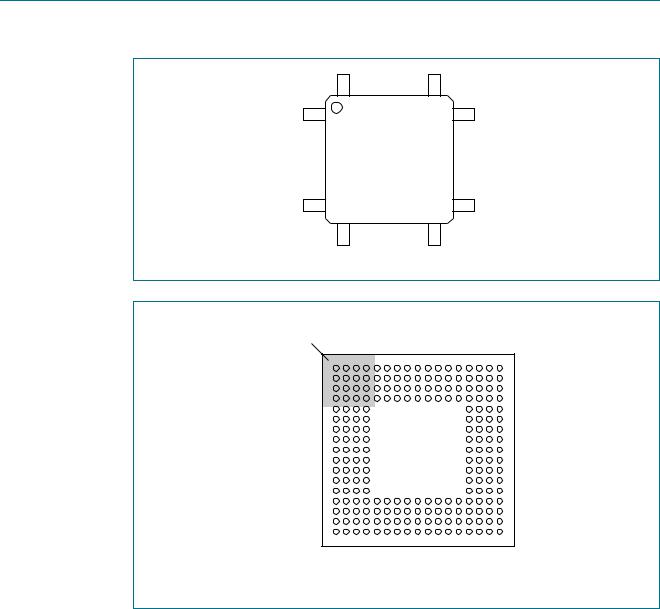
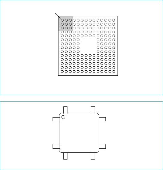
6.Pinning information
6.1Pinning
208 |
157 |
1 |
156 |
LPC178x/7xFBD208
52
53
104
105
002aaf518
Fig 2. Pin configuration (LQFP208)
ball A1 |
|
|
|
|
|
|
|
|
index area |
2 |
4 |
6 |
8 |
10 12 |
14 16 |
|
|
1 |
3 |
5 |
7 |
9 |
11 |
13 |
15 |
17 |
A |
|
|
|
|
|
|
|
|
B |
|
|
|
|
|
|
|
|
C |
|
|
|
|
|
|
|
|
D |
|
|
|
|
|
|
|
|
E |
|
|
|
|
|
|
|
|
F |
|
|
|
|
|
|
|
|
G |
|
|
|
|
|
|
|
|
H |
|
|
LPC178x/7x |
|
|
|
||
J |
|
|
|
|
|
|||
K |
|
|
|
|
|
|
|
|
L |
|
|
|
|
|
|
|
|
M |
|
|
|
|
|
|
|
|
N |
|
|
|
|
|
|
|
|
P |
|
|
|
|
|
|
|
|
R |
|
|
|
|
|
|
|
|
T |
|
|
|
|
|
|
|
|
U |
|
|
|
|
|
|
|
|
002aaf529
Transparent top view
Fig 3. Pin configuration (TFBGA208)
LPC178X_7X |
All information provided in this document is subject to legal disclaimers. |
© NXP Semiconductors N.V. 2014. All rights reserved. |
Product data sheet |
Rev. 5 — 9 September 2014 |
8 of 122 |
NXP Semiconductors |
LPC178x/7x |
|
32-bit ARM Cortex-M3 microcontroller |
ball A1 |
LPC178x/7x |
index area |
|
1 2 3 4 5 6 7 8 9 10 11 12 13 14
A
B
C
D
E
F
G
H
J
K
L
M
N
P
002aaf519
Transparent top view
Fig 4. Pin configuration (TFBGA180)
144 |
109 |
1 |
108 |
LPC178x/7x
36
37
Fig 5. Pin configuration (LQFP144)
72
73
002aaf520
6.2 Pin description
I/O pins on the LPC178x/7x are 5 V tolerant and have input hysteresis unless otherwise indicated in the table below. Crystal pins, power pins, and reference voltage pins are not 5 V tolerant. In addition, when pins are selected to be ADC inputs, they are no longer 5 V tolerant and the input voltage must be limited to the voltage at the ADC positive reference pin (VREFP).
All port pins Pn[m] are multiplexed, and the multiplexed functions appear in Table 3 in the order defined by the FUNC bits of the corresponding IOCON register up to the highest used function number. Each port pin can support up to eight multiplexed functions. IOCON register FUNC values which are reserved are noted as ‘R’ in the pin configuration table.
LPC178X_7X |
All information provided in this document is subject to legal disclaimers. |
© NXP Semiconductors N.V. 2014. All rights reserved. |
Product data sheet |
Rev. 5 — 9 September 2014 |
9 of 122 |
NXP Semiconductors |
LPC178x/7x |
|
32-bit ARM Cortex-M3 microcontroller |
Table 3. Pin description
Not all functions are available on all parts. See Table 2 (Ethernet, USB, LCD, QEI, SD/MMC, DAC pins) and Table 7 (EMC pins).
Symbol |
Pin LQFP208 |
Ball TFBGA208 |
Ball TFBGA180 |
Pin LQFP144 |
|
|
|
|
|
|
|
Description |
|
|
Reset state[1] |
|
|
Type[2] |
|
|
|
||||
|
|
|
|
|
|
|||||||
|
|
|
|
|
|
|||||||
|
|
|
|
|
|
|||||||
P0[0] to |
|
|
|
|
|
|
|
|
I/O |
Port 0: Port 0 is a 32-bit I/O port with individual direction |
||
P0[31] |
|
|
|
|
|
|
|
|
|
|
|
controls for each bit. The operation of port 0 pins depends upon |
|
|
|
|
|
|
|
|
|
|
|
|
the pin function selected via the pin connect block. |
|
|
|
|
|
|
|
|
|
||||
P0[0] |
94 |
U15 |
M10 |
66 |
[3] |
I; |
I/O |
P0[0] — General purpose digital input/output pin. |
||||
|
|
|
|
|
|
PU |
|
|
|
|
||
|
|
|
|
|
|
I |
CAN_RD1 — CAN1 receiver input. |
|||||
|
|
|
|
|
|
|
|
|
||||
|
|
|
|
|
|
|
|
|
|
|
||
|
|
|
|
|
|
|
|
|
O |
U3_TXD — Transmitter output for UART3. |
||
|
|
|
|
|
|
|
|
|
|
|
||
|
|
|
|
|
|
|
|
|
I/O |
I2C1_SDA — I2C1 data input/output (this pin does not use a |
||
|
|
|
|
|
|
|
|
|
|
|
|
specialized I2C pad). |
|
|
|
|
|
|
|
|
|
|
|
||
|
|
|
|
|
|
|
|
|
O |
U0_TXD — Transmitter output for UART0. |
||
|
|
|
|
|
|
|
|
|
||||
P0[1] |
96 |
T14 |
N11 |
67 |
[3] |
I; |
I/O |
P0[1] — General purpose digital input/output pin. |
||||
|
|
|
|
|
|
PU |
|
|
|
|
||
|
|
|
|
|
|
O |
CAN_TD1 — CAN1 transmitter output. |
|||||
|
|
|
|
|
|
|
|
|
||||
|
|
|
|
|
|
|
|
|
|
|
||
|
|
|
|
|
|
|
|
|
I |
U3_RXD — Receiver input for UART3. |
||
|
|
|
|
|
|
|
|
|
|
|
||
|
|
|
|
|
|
|
|
|
I/O |
I2C1_SCL — I2C1 clock input/output (this pin does not use a |
||
|
|
|
|
|
|
|
|
|
|
|
|
specialized I2C pad). |
|
|
|
|
|
|
|
|
|
|
|
||
|
|
|
|
|
|
|
|
|
I |
U0_RXD — Receiver input for UART0. |
||
|
|
|
|
|
|
|
|
|
||||
P0[2] |
202 |
C4 |
D5 |
141 |
[3] |
I; |
I/O |
P0[2] — General purpose digital input/output pin. |
||||
|
|
|
|
|
|
PU |
|
|
|
|
||
|
|
|
|
|
|
O |
U0_TXD — Transmitter output for UART0. |
|||||
|
|
|
|
|
|
|
|
|
||||
|
|
|
|
|
|
|
|
|
|
|
||
|
|
|
|
|
|
|
|
|
O |
U3_TXD — Transmitter output for UART3. |
||
|
|
|
|
|
|
|
|
|
||||
P0[3] |
204 |
D6 |
A3 |
142 |
[3] |
I; |
I/O |
P0[3] — General purpose digital input/output pin. |
||||
|
|
|
|
|
|
PU |
|
|
|
|
||
|
|
|
|
|
|
I |
U0_RXD — Receiver input for UART0. |
|||||
|
|
|
|
|
|
|
|
|
||||
|
|
|
|
|
|
|
|
|
|
|
||
|
|
|
|
|
|
|
|
|
I |
U3_RXD — Receiver input for UART3. |
||
|
|
|
|
|
|
|
|
|
||||
P0[4] |
168 |
B12 |
A11 |
116 |
[3] |
I; |
I/O |
P0[4] — General purpose digital input/output pin. |
||||
|
|
|
|
|
|
PU |
|
|
||||
|
|
|
|
|
|
I/O |
I2S_RX_SCK — I2S Receive clock. It is driven by the master |
|||||
|
|
|
|
|
|
|
|
|
|
|
|
and received by the slave. Corresponds to the signal SCK in the |
|
|
|
|
|
|
|
|
|
|
|
|
I2S-bus specification. |
|
|
|
|
|
|
|
|
|
I |
CAN_RD2 — CAN2 receiver input. |
||
|
|
|
|
|
|
|
|
|
|
|
||
|
|
|
|
|
|
|
|
|
I |
T2_CAP0 — Capture input for Timer 2, channel 0. |
||
|
|
|
|
|
|
|
|
|
|
|
|
|
|
|
|
|
|
|
|
|
|
- |
|
|
R — Function reserved. |
|
|
|
|
|
|
|
|
|
|
|
|
|
|
|
|
|
|
|
|
|
|
- |
|
|
R — Function reserved. |
|
|
|
|
|
|
|
|
|
|
|
|
|
|
|
|
|
|
|
|
|
|
- |
|
|
R — Function reserved. |
|
|
|
|
|
|
|
|
|
|
|
||
|
|
|
|
|
|
|
|
|
O |
LCD_VD[0] — LCD data. |
||
|
|
|
|
|
|
|
|
|
|
|
|
|
LPC178X_7X |
All information provided in this document is subject to legal disclaimers. |
© NXP Semiconductors N.V. 2014. All rights reserved. |
Product data sheet |
Rev. 5 — 9 September 2014 |
10 of 122 |
NXP Semiconductors |
LPC178x/7x |
|
32-bit ARM Cortex-M3 microcontroller |
Table 3. Pin description …continued
Not all functions are available on all parts. See Table 2 (Ethernet, USB, LCD, QEI, SD/MMC, DAC pins) and Table 7 (EMC pins).
Symbol |
Pin LQFP208 |
Ball TFBGA208 |
Ball TFBGA180 |
Pin LQFP144 |
|
Reset state[1] |
|
|
|
|
|
Description |
|
|
|
|
|
|
|
|
|||||
|
|
|
|
|
||||||||
|
|
|
|
Type[2] |
|
|
|
|||||
|
|
|
|
|
|
|||||||
P0[5] |
166 |
C12 |
B11 |
115 |
[3] |
I; |
I/O |
P0[5] — General purpose digital input/output pin. |
||||
|
|
|
|
|
|
PU |
|
|
||||
|
|
|
|
|
|
I/O |
I2S_RX_WS — I2S Receive word select. It is driven by the |
|||||
|
|
|
|
|
|
|
|
|
|
|
|
master and received by the slave. Corresponds to the signal WS |
|
|
|
|
|
|
|
|
|
|
|
|
in the I2S-bus specification. |
|
|
|
|
|
|
|
|
|
O |
CAN_TD2 — CAN2 transmitter output. |
||
|
|
|
|
|
|
|
|
|
|
|
||
|
|
|
|
|
|
|
|
|
I |
T2_CAP1 — Capture input for Timer 2, channel 1. |
||
|
|
|
|
|
|
|
|
|
|
|
|
|
|
|
|
|
|
|
|
|
|
- |
|
|
R — Function reserved. |
|
|
|
|
|
|
|
|
|
|
|
|
|
|
|
|
|
|
|
|
|
|
- |
|
|
R — Function reserved. |
|
|
|
|
|
|
|
|
|
|
|
|
|
|
|
|
|
|
|
|
|
|
- |
|
|
R — Function reserved. |
|
|
|
|
|
|
|
|
|
|
|
||
|
|
|
|
|
|
|
|
|
O |
LCD_VD[1] — LCD data. |
||
|
|
|
|
|
|
|
|
|
||||
P0[6] |
164 |
D13 |
D11 |
113 |
[3] |
I; |
I/O |
P0[6] — General purpose digital input/output pin. |
||||
|
|
|
|
|
|
PU |
|
|
||||
|
|
|
|
|
|
I/O |
I2S_RX_SDA — I2S Receive data. It is driven by the transmitter |
|||||
|
|
|
|
|
|
|
|
|
|
|
|
and read by the receiver. Corresponds to the signal SD in the |
|
|
|
|
|
|
|
|
|
|
|
|
I2S-bus specification. |
|
|
|
|
|
|
|
|
|
I/O |
SSP1_SSEL — Slave Select for SSP1. |
||
|
|
|
|
|
|
|
|
|
|
|
||
|
|
|
|
|
|
|
|
|
O |
T2_MAT0 — Match output for Timer 2, channel 0. |
||
|
|
|
|
|
|
|
|
|
|
|
||
|
|
|
|
|
|
|
|
|
O |
U1_RTS — Request to Send output for UART1. Can also be |
||
|
|
|
|
|
|
|
|
|
|
|
|
configured to be an RS-485/EIA-485 output enable signal for |
|
|
|
|
|
|
|
|
|
|
|
|
UART1. |
|
|
|
|
|
|
|
|
|
|
|
|
|
|
|
|
|
|
|
|
|
|
- |
|
|
R — Function reserved. |
|
|
|
|
|
|
|
|
|
|
|
|
|
|
|
|
|
|
|
|
|
|
- |
|
|
R — Function reserved. |
|
|
|
|
|
|
|
|
|
|
|
||
|
|
|
|
|
|
|
|
|
O |
LCD_VD[8] — LCD data. |
||
|
|
|
|
|
|
|
|
|
||||
P0[7] |
162 |
C13 |
B12 |
112 |
[4] |
I; IA |
I/O |
P0[7] — General purpose digital input/output pin. |
||||
|
|
|
|
|
|
|
|
|
|
|
||
|
|
|
|
|
|
|
|
|
I/O |
I2S_TX_SCK — I2S transmit clock. It is driven by the master |
||
|
|
|
|
|
|
|
|
|
|
|
|
and received by the slave. Corresponds to the signal SCK in the |
|
|
|
|
|
|
|
|
|
|
|
|
I2S-bus specification. |
|
|
|
|
|
|
|
|
|
I/O |
SSP1_SCK — Serial Clock for SSP1. |
||
|
|
|
|
|
|
|
|
|
|
|
||
|
|
|
|
|
|
|
|
|
O |
T2_MAT1 — Match output for Timer 2, channel 1. |
||
|
|
|
|
|
|
|
|
|
|
|
||
|
|
|
|
|
|
|
|
|
I |
RTC_EV0 — Event input 0 to Event Monitor/Recorder. |
||
|
|
|
|
|
|
|
|
|
|
|
|
|
|
|
|
|
|
|
|
|
|
- |
|
|
R — Function reserved. |
|
|
|
|
|
|
|
|
|
|
|
|
|
|
|
|
|
|
|
|
|
|
- |
|
|
R — Function reserved. |
|
|
|
|
|
|
|
|
|
|
|
||
|
|
|
|
|
|
|
|
|
O |
LCD_VD[9] — LCD data. |
||
|
|
|
|
|
|
|
|
|
|
|
|
|
LPC178X_7X |
All information provided in this document is subject to legal disclaimers. |
© NXP Semiconductors N.V. 2014. All rights reserved. |
Product data sheet |
Rev. 5 — 9 September 2014 |
11 of 122 |
NXP Semiconductors |
LPC178x/7x |
|
32-bit ARM Cortex-M3 microcontroller |
Table 3. Pin description …continued
Not all functions are available on all parts. See Table 2 (Ethernet, USB, LCD, QEI, SD/MMC, DAC pins) and Table 7 (EMC pins).
Symbol |
Pin LQFP208 |
Ball TFBGA208 |
Ball TFBGA180 |
Pin LQFP144 |
|
Reset state[1] |
|
|
|
|
|
|
Description |
|
|
|
|
|
|
|
|
|
|
|
|||||
|
|
|
|
|
|
|
||||||||
|
|
|
|
Type[2] |
|
|
|
|
|
|||||
|
|
|
|
|
|
|
|
|||||||
P0[8] |
160 |
A15 |
C12 |
111 |
[4] |
I; IA |
I/O |
|
P0[8] — General purpose digital input/output pin. |
|||||
|
|
|
|
|
|
|
|
|
|
|
||||
|
|
|
|
|
|
|
|
|
I/O |
I2S_TX_WS — I2S Transmit word select. It is driven by the |
||||
|
|
|
|
|
|
|
|
|
|
|
|
|
master and received by the slave. Corresponds to the signal WS |
|
|
|
|
|
|
|
|
|
|
|
|
|
|
in the I2S-bus specification. |
|
|
|
|
|
|
|
|
|
|
I/O |
SSP1_MISO — Master In Slave Out for SSP1. |
||||
|
|
|
|
|
|
|
|
|
|
|
||||
|
|
|
|
|
|
|
|
|
O |
T2_MAT2 — Match output for Timer 2, channel 2. |
||||
|
|
|
|
|
|
|
|
|
|
|
||||
|
|
|
|
|
|
|
|
|
I |
RTC_EV1 — Event input 1 to Event Monitor/Recorder. |
||||
|
|
|
|
|
|
|
|
|
|
|
|
|
||
|
|
|
|
|
|
|
|
|
- |
|
|
R — Function reserved. |
||
|
|
|
|
|
|
|
|
|
|
|
|
|
||
|
|
|
|
|
|
|
|
|
- |
|
|
R — Function reserved. |
||
|
|
|
|
|
|
|
|
|
|
|
||||
|
|
|
|
|
|
|
|
|
O |
LCD_VD[16] — LCD data. |
||||
|
|
|
|
|
|
|
|
|
|
|||||
P0[9] |
158 |
C14 |
A13 |
109 |
[4] |
I; IA |
I/O |
|
P0[9] — General purpose digital input/output pin. |
|||||
|
|
|
|
|
|
|
|
|
|
|
||||
|
|
|
|
|
|
|
|
|
I/O |
I2S_TX_SDA — I2S transmit data. It is driven by the transmitter |
||||
|
|
|
|
|
|
|
|
|
|
|
|
|
and read by the receiver. Corresponds to the signal SD in the |
|
|
|
|
|
|
|
|
|
|
|
|
|
|
I2S-bus specification. |
|
|
|
|
|
|
|
|
|
|
I/O |
SSP1_MOSI — Master Out Slave In for SSP1. |
||||
|
|
|
|
|
|
|
|
|
|
|
||||
|
|
|
|
|
|
|
|
|
O |
T2_MAT3 — Match output for Timer 2, channel 3. |
||||
|
|
|
|
|
|
|
|
|
|
|
||||
|
|
|
|
|
|
|
|
|
I |
RTC_EV2 — Event input 2 to Event Monitor/Recorder. |
||||
|
|
|
|
|
|
|
|
|
|
|
|
|
||
|
|
|
|
|
|
|
|
|
- |
|
|
R — Function reserved. |
||
|
|
|
|
|
|
|
|
|
|
|
|
|
||
|
|
|
|
|
|
|
|
|
- |
|
|
R — Function reserved. |
||
|
|
|
|
|
|
|
|
|
|
|
||||
|
|
|
|
|
|
|
|
|
O |
LCD_VD[17] — LCD data. |
||||
|
|
|
|
|
|
|
|
|
|
|||||
P0[10] |
98 |
T15 |
L10 |
69 |
[3] |
I; |
I/O |
|
P0[10] — General purpose digital input/output pin. |
|||||
|
|
|
|
|
|
PU |
|
|
|
|
|
|
||
|
|
|
|
|
|
O |
|
U2_TXD — Transmitter output for UART2. |
||||||
|
|
|
|
|
|
|
|
|
|
|||||
|
|
|
|
|
|
|
|
|
|
|
|
|||
|
|
|
|
|
|
|
|
|
I/O |
|
I2C2_SDA — I2C2 data input/output (this pin does not use a |
|||
|
|
|
|
|
|
|
|
|
|
|
|
|
specialized I2C pad). |
|
|
|
|
|
|
|
|
|
|
|
|
|
|||
|
|
|
|
|
|
|
|
|
O |
|
T3_MAT0 — Match output for Timer 3, channel 0. |
|||
|
|
|
|
|
|
|
|
|
|
|||||
P0[11] |
100 |
R14 |
P12 |
70 |
[3] |
I; |
I/O |
|
P0[11] — General purpose digital input/output pin. |
|||||
|
|
|
|
|
|
PU |
|
|
|
|
|
|
||
|
|
|
|
|
|
I |
U2_RXD — Receiver input for UART2. |
|||||||
|
|
|
|
|
|
|
|
|
||||||
|
|
|
|
|
|
|
|
|
|
|
||||
|
|
|
|
|
|
|
|
|
I/O |
I2C2_SCL — I2C2 clock input/output (this pin does not use a |
||||
|
|
|
|
|
|
|
|
|
|
|
|
|
specialized I2C pad). |
|
|
|
|
|
|
|
|
|
|
|
|
|
|||
|
|
|
|
|
|
|
|
|
O |
|
T3_MAT1 — Match output for Timer 3, channel 1. |
|||
|
|
|
|
|
|
|
|
|
|
|||||
P0[12] |
41 |
R1 |
J4 |
29 |
[5] |
I; |
I/O |
|
P0[12] — General purpose digital input/output pin. |
|||||
|
|
|
|
|
|
PU |
|
|
|
|
|
|
||
|
|
|
|
|
|
O |
|
USB_PPWR2 — Port Power enable signal for USB port 2. |
||||||
|
|
|
|
|
|
|
|
|
|
|||||
|
|
|
|
|
|
|
|
|
|
|
||||
|
|
|
|
|
|
|
|
|
I/O |
SSP1_MISO — Master In Slave Out for SSP1. |
||||
|
|
|
|
|
|
|
|
|
|
|
||||
|
|
|
|
|
|
|
|
|
I |
ADC0_IN[6] — A/D converter 0, input 6. When configured as an |
||||
|
|
|
|
|
|
|
|
|
|
|
|
ADC input, the digital function of the pin must be disabled. |
||
|
|
|
|
|
|
|
|
|
|
|
|
|
|
|
LPC178X_7X |
All information provided in this document is subject to legal disclaimers. |
© NXP Semiconductors N.V. 2014. All rights reserved. |
Product data sheet |
Rev. 5 — 9 September 2014 |
12 of 122 |
NXP Semiconductors |
LPC178x/7x |
|
32-bit ARM Cortex-M3 microcontroller |
Table 3. Pin description …continued
Not all functions are available on all parts. See Table 2 (Ethernet, USB, LCD, QEI, SD/MMC, DAC pins) and Table 7 (EMC pins).
Symbol |
Pin LQFP208 |
Ball TFBGA208 |
Ball TFBGA180 |
Pin LQFP144 |
|
Reset state[1] |
|
|
|
|
|
|
Description |
|
|
|
|
|
|
|
|
|
|
|
|||||
|
|
|
|
|
|
|
||||||||
|
|
|
|
Type[2] |
|
|
|
|
|
|||||
|
|
|
|
|
|
|
|
|||||||
P0[13] |
45 |
R2 |
J5 |
32 |
[5] |
I; |
I/O |
|
P0[13] — General purpose digital input/output pin. |
|||||
|
|
|
|
|
|
PU |
|
|
|
|
|
|
||
|
|
|
|
|
|
O |
|
USB_UP_LED2 — USB port 2 GoodLink LED indicator. It is |
||||||
|
|
|
|
|
|
|
|
|
|
|||||
|
|
|
|
|
|
|
|
|
|
|
|
|
LOW when the device is configured (non-control endpoints |
|
|
|
|
|
|
|
|
|
|
|
|
|
|
enabled), or when the host is enabled and has detected a |
|
|
|
|
|
|
|
|
|
|
|
|
|
|
device on the bus. It is HIGH when the device is not configured, |
|
|
|
|
|
|
|
|
|
|
|
|
|
|
or when host is enabled and has not detected a device on the |
|
|
|
|
|
|
|
|
|
|
|
|
|
|
bus, or during global suspend. It transitions between LOW and |
|
|
|
|
|
|
|
|
|
|
|
|
|
|
HIGH (flashes) when the host is enabled and detects activity on |
|
|
|
|
|
|
|
|
|
|
|
|
|
|
the bus. |
|
|
|
|
|
|
|
|
|
|
|
|
|
|||
|
|
|
|
|
|
|
|
|
I/O |
|
SSP1_MOSI — Master Out Slave In for SSP1. |
|||
|
|
|
|
|
|
|
|
|
|
|
||||
|
|
|
|
|
|
|
|
|
I |
ADC0_IN[7] — A/D converter 0, input 7. When configured as an |
||||
|
|
|
|
|
|
|
|
|
|
|
|
|
ADC input, the digital function of the pin must be disabled. |
|
|
|
|
|
|
|
|
|
|
|
|||||
P0[14] |
69 |
T7 |
M5 |
48 |
[3] |
I; |
I/O |
|
P0[14] — General purpose digital input/output pin. |
|||||
|
|
|
|
|
|
PU |
|
|
|
|
|
|
||
|
|
|
|
|
|
O |
|
USB_HSTEN2 — Host Enabled status for USB port 2. |
||||||
|
|
|
|
|
|
|
|
|
|
|||||
|
|
|
|
|
|
|
|
|
|
|
|
|||
|
|
|
|
|
|
|
|
|
I/O |
|
SSP1_SSEL — Slave Select for SSP1. |
|||
|
|
|
|
|
|
|
|
|
|
|
||||
|
|
|
|
|
|
|
|
|
O |
USB_CONNECT2 — SoftConnect control for USB port 2. |
||||
|
|
|
|
|
|
|
|
|
|
|
|
Signal used to switch an external 1.5 k resistor under software |
||
|
|
|
|
|
|
|
|
|
|
|
|
|
control. Used with the SoftConnect USB feature. |
|
|
|
|
|
|
|
|
|
|
|
|||||
P0[15] |
128 |
J16 |
H13 |
89 |
[3] |
I; |
I/O |
|
P0[15] — General purpose digital input/output pin. |
|||||
|
|
|
|
|
|
PU |
|
|
|
|
|
|
||
|
|
|
|
|
|
O |
|
U1_TXD — Transmitter output for UART1. |
||||||
|
|
|
|
|
|
|
|
|
|
|||||
|
|
|
|
|
|
|
|
|
|
|
|
|||
|
|
|
|
|
|
|
|
|
I/O |
|
SSP0_SCK — Serial clock for SSP0. |
|||
|
|
|
|
|
|
|
|
|
|
|||||
P0[16] |
130 |
J14 |
H14 |
90 |
[3] |
I; |
I/O |
|
P0[16] — General purpose digital input/output pin. |
|||||
|
|
|
|
|
|
PU |
|
|
|
|
|
|
||
|
|
|
|
|
|
I |
|
U1_RXD — Receiver input for UART1. |
||||||
|
|
|
|
|
|
|
|
|
|
|||||
|
|
|
|
|
|
|
|
|
|
|
||||
|
|
|
|
|
|
|
|
|
I/O |
SSP0_SSEL — Slave Select for SSP0. |
||||
|
|
|
|
|
|
|
|
|
|
|||||
P0[17] |
126 |
K17 |
J12 |
87 |
[3] |
I; |
I/O |
|
P0[17] — General purpose digital input/output pin. |
|||||
|
|
|
|
|
|
PU |
|
|
|
|
|
|
||
|
|
|
|
|
|
I |
|
U1_CTS — Clear to Send input for UART1. |
||||||
|
|
|
|
|
|
|
|
|
|
|||||
|
|
|
|
|
|
|
|
|
|
|
|
|||
|
|
|
|
|
|
|
|
|
I/O |
|
SSP0_MISO — Master In Slave Out for SSP0. |
|||
|
|
|
|
|
|
|
|
|
|
|||||
P0[18] |
124 |
K15 |
J13 |
86 |
[3] |
I; |
I/O |
|
P0[18] — General purpose digital input/output pin. |
|||||
|
|
|
|
|
|
PU |
|
|
|
|
|
|
||
|
|
|
|
|
|
I |
|
U1_DCD — Data Carrier Detect input for UART1. |
||||||
|
|
|
|
|
|
|
|
|
|
|||||
|
|
|
|
|
|
|
|
|
|
|
|
|||
|
|
|
|
|
|
|
|
|
I/O |
|
SSP0_MOSI — Master Out Slave In for SSP0. |
|||
|
|
|
|
|
|
|
|
|
|
|||||
P0[19] |
122 |
L17 |
J10 |
85 |
[3] |
I; |
I/O |
|
P0[19] — General purpose digital input/output pin. |
|||||
|
|
|
|
|
|
PU |
|
|
|
|
|
|
||
|
|
|
|
|
|
I |
|
U1_DSR — Data Set Ready input for UART1. |
||||||
|
|
|
|
|
|
|
|
|
|
|||||
|
|
|
|
|
|
|
|
|
|
|
||||
|
|
|
|
|
|
|
|
|
O |
SD_CLK — Clock output line for SD card interface. |
||||
|
|
|
|
|
|
|
|
|
|
|
||||
|
|
|
|
|
|
|
|
|
I/O |
I2C1_SDA — I2C1 data input/output (this pin does not use a |
||||
|
|
|
|
|
|
|
|
|
|
|
|
|
specialized I2C pad). |
|
|
|
|
|
|
|
|
|
|
|
|
|
|
|
|
LPC178X_7X |
All information provided in this document is subject to legal disclaimers. |
© NXP Semiconductors N.V. 2014. All rights reserved. |
Product data sheet |
Rev. 5 — 9 September 2014 |
13 of 122 |
NXP Semiconductors |
LPC178x/7x |
|
32-bit ARM Cortex-M3 microcontroller |
Table 3. Pin description …continued
Not all functions are available on all parts. See Table 2 (Ethernet, USB, LCD, QEI, SD/MMC, DAC pins) and Table 7 (EMC pins).
Symbol |
Pin LQFP208 |
Ball TFBGA208 |
Ball TFBGA180 |
Pin LQFP144 |
|
Reset state[1] |
|
|
|
|
|
Description |
|
|
|
|
|
|
|
|
|||||
|
|
|
|
|
||||||||
|
|
|
|
Type[2] |
|
|
|
|||||
|
|
|
|
|
|
|||||||
P0[20] |
120 |
M17 |
K14 |
83 |
[3] |
I; |
I/O |
P0[20] — General purpose digital input/output pin. |
||||
|
|
|
|
|
|
PU |
|
|
|
|
||
|
|
|
|
|
|
O |
U1_DTR — Data Terminal Ready output for UART1. Can also |
|||||
|
|
|
|
|
|
|
|
|
||||
|
|
|
|
|
|
|
|
|
|
|
|
be configured to be an RS-485/EIA-485 output enable signal for |
|
|
|
|
|
|
|
|
|
|
|
|
UART1. |
|
|
|
|
|
|
|
|
|
|
|
||
|
|
|
|
|
|
|
|
|
I/O |
SD_CMD — Command line for SD card interface. |
||
|
|
|
|
|
|
|
|
|
|
|
||
|
|
|
|
|
|
|
|
|
I/O |
I2C1_SCL — I2C1 clock input/output (this pin does not use a |
||
|
|
|
|
|
|
|
|
|
|
|
|
specialized I2C pad). |
|
|
|
|
|
|
|
|
|
||||
P0[21] |
118 |
M16 |
K11 |
82 |
[3] |
I; |
I/O |
P0[21] — General purpose digital input/output pin. |
||||
|
|
|
|
|
|
PU |
|
|
|
|
||
|
|
|
|
|
|
I |
U1_RI — Ring Indicator input for UART1. |
|||||
|
|
|
|
|
|
|
|
|
||||
|
|
|
|
|
|
|
|
|
|
|
||
|
|
|
|
|
|
|
|
|
O |
SD_PWR — Power Supply Enable for external SD card power |
||
|
|
|
|
|
|
|
|
|
|
|
|
supply. |
|
|
|
|
|
|
|
|
|
|
|
||
|
|
|
|
|
|
|
|
|
O |
U4_OE — RS-485/EIA-485 output enable signal for UART4. |
||
|
|
|
|
|
|
|
|
|
|
|
||
|
|
|
|
|
|
|
|
|
I |
CAN_RD1 — CAN1 receiver input. |
||
|
|
|
|
|
|
|
|
|
|
|
||
|
|
|
|
|
|
|
|
|
I/O |
U4_SCLK — USART 4 clock input or output in synchronous |
||
|
|
|
|
|
|
|
|
|
|
|
|
mode. |
|
|
|
|
|
|
|
|
|
||||
P0[22] |
116 |
N17 |
L14 |
80 |
[6] |
I; |
I/O |
P0[22] — General purpose digital input/output pin. |
||||
|
|
|
|
|
|
PU |
|
|
|
|
||
|
|
|
|
|
|
O |
U1_RTS — Request to Send output for UART1. Can also be |
|||||
|
|
|
|
|
|
|
|
|
||||
|
|
|
|
|
|
|
|
|
|
|
|
configured to be an RS-485/EIA-485 output enable signal for |
|
|
|
|
|
|
|
|
|
|
|
|
UART1. |
|
|
|
|
|
|
|
|
|
|
|
||
|
|
|
|
|
|
|
|
|
I/O |
SD_DAT[0] — Data line 0 for SD card interface. |
||
|
|
|
|
|
|
|
|
|
|
|
||
|
|
|
|
|
|
|
|
|
O |
U4_TXD — Transmitter output for USART4 (input/output in |
||
|
|
|
|
|
|
|
|
|
|
|
|
smart card mode). |
|
|
|
|
|
|
|
|
|
|
|
||
|
|
|
|
|
|
|
|
|
O |
CAN_TD1 — CAN1 transmitter output. |
||
|
|
|
|
|
|
|
|
|
||||
P0[23] |
18 |
H1 |
F5 |
13 |
[5] |
I; |
I/O |
P0[23] — General purpose digital input/output pin. |
||||
|
|
|
|
|
|
PU |
|
|
|
|
||
|
|
|
|
|
|
I |
ADC0_IN[0] — A/D converter 0, input 0. When configured as an |
|||||
|
|
|
|
|
|
|
|
|
||||
|
|
|
|
|
|
|
|
|
|
|
|
ADC input, the digital function of the pin must be disabled. |
|
|
|
|
|
|
|
|
|
|
|
||
|
|
|
|
|
|
|
|
|
I/O |
I2S_RX_SCK — Receive Clock. It is driven by the master and |
||
|
|
|
|
|
|
|
|
|
|
|
|
received by the slave. Corresponds to the signal SCK in the |
|
|
|
|
|
|
|
|
|
|
|
|
I2S-bus specification. |
|
|
|
|
|
|
|
|
|
I |
T3_CAP0 — Capture input for Timer 3, channel 0. |
||
|
|
|
|
|
|
|
|
|
||||
P0[24] |
16 |
G2 |
E1 |
11 |
[5] |
I; |
I/O |
P0[24] — General purpose digital input/output pin. |
||||
|
|
|
|
|
|
PU |
|
|
|
|
||
|
|
|
|
|
|
I |
ADC0_IN[1] — A/D converter 0, input 1. When configured as an |
|||||
|
|
|
|
|
|
|
|
|
||||
|
|
|
|
|
|
|
|
|
|
|
|
ADC input, the digital function of the pin must be disabled. |
|
|
|
|
|
|
|
|
|
|
|
||
|
|
|
|
|
|
|
|
|
I/O |
I2S_RX_WS — Receive Word Select. It is driven by the master |
||
|
|
|
|
|
|
|
|
|
|
|
|
and received by the slave. Corresponds to the signal WS in the |
|
|
|
|
|
|
|
|
|
|
|
|
I2S-bus specification. |
|
|
|
|
|
|
|
|
|
I |
T3_CAP1 — Capture input for Timer 3, channel 1. |
||
|
|
|
|
|
|
|
|
|
|
|
|
|
LPC178X_7X |
All information provided in this document is subject to legal disclaimers. |
© NXP Semiconductors N.V. 2014. All rights reserved. |
Product data sheet |
Rev. 5 — 9 September 2014 |
14 of 122 |
NXP Semiconductors |
LPC178x/7x |
|
32-bit ARM Cortex-M3 microcontroller |
Table 3. Pin description …continued
Not all functions are available on all parts. See Table 2 (Ethernet, USB, LCD, QEI, SD/MMC, DAC pins) and Table 7 (EMC pins).
Symbol |
Pin LQFP208 |
Ball TFBGA208 |
Ball TFBGA180 |
Pin LQFP144 |
|
Reset state[1] |
|
|
|
|
|
|
Description |
|
||
|
|
|
|
|
|
|
|
|
|
|
|
|||||
|
|
|
|
|
|
|
|
|
||||||||
|
|
|
|
Type[2] |
|
|
|
|
|
|
|
|||||
|
|
|
|
|
|
|
|
|
|
|||||||
P0[25] |
14 |
F1 |
E4 |
10 |
[5] |
I; |
I/O |
|
P0[25] — General purpose digital input/output pin. |
|||||||
|
|
|
|
|
|
PU |
|
|
|
|
|
|
|
|
||
|
|
|
|
|
|
I |
|
ADC0_IN[2] — A/D converter 0, input 2. When configured as an |
||||||||
|
|
|
|
|
|
|
|
|
|
|||||||
|
|
|
|
|
|
|
|
|
|
|
|
|
ADC input, the digital function of the pin must be disabled. |
|||
|
|
|
|
|
|
|
|
|
|
|
|
|||||
|
|
|
|
|
|
|
|
|
I/O |
|
I2S_RX_SDA — Receive data. It is driven by the transmitter |
|||||
|
|
|
|
|
|
|
|
|
|
|
|
|
and read by the receiver. Corresponds to the signal SD in the |
|||
|
|
|
|
|
|
|
|
|
|
|
|
|
I2S-bus specification. |
|
||
|
|
|
|
|
|
|
|
|
O |
U3_TXD — Transmitter output for UART3. |
||||||
|
|
|
|
|
|
|
|
|
|
|||||||
P0[26] |
12 |
E1 |
D1 |
8 |
[7] |
I; |
I/O |
|
P0[26] — General purpose digital input/output pin. |
|||||||
|
|
|
|
|
|
PU |
|
|
|
|
|
|
|
|
||
|
|
|
|
|
|
I |
|
ADC0_IN[3] — A/D converter 0, input 3. When configured as an |
||||||||
|
|
|
|
|
|
|
|
|
|
|||||||
|
|
|
|
|
|
|
|
|
|
|
|
|
ADC input, the digital function of the pin must be disabled. |
|||
|
|
|
|
|
|
|
|
|
|
|
|
|||||
|
|
|
|
|
|
|
|
|
O |
|
DAC_OUT — D/A converter output. When configured as the |
|||||
|
|
|
|
|
|
|
|
|
|
|
|
|
DAC output, the digital function of the pin must be disabled. |
|||
|
|
|
|
|
|
|
|
|
|
|
|
|||||
|
|
|
|
|
|
|
|
|
I |
|
U3_RXD — Receiver input for UART3. |
|||||
|
|
|
|
|
|
|
|
|
|
|||||||
P0[27] |
50 |
T1 |
L3 |
35 |
[8] |
I |
I/O |
|
P0[27] — General purpose digital input/output pin. |
|||||||
|
|
|
|
|
|
|
|
|
|
|
|
|||||
|
|
|
|
|
|
|
|
|
I/O |
|
I2C0_SDA — I2C0 data input/output (this pin uses a specialized |
|||||
|
|
|
|
|
|
|
|
|
|
|
|
|
I2C pad). |
|
||
|
|
|
|
|
|
|
|
|
|
|
|
|||||
|
|
|
|
|
|
|
|
|
I/O |
|
USB_SDA1 — I2C serial data for communication with an |
|||||
|
|
|
|
|
|
|
|
|
|
|
|
|
external USB transceiver. |
|
||
|
|
|
|
|
|
|
|
|
|
|||||||
P0[28] |
48 |
R3 |
M1 |
34 |
[8] |
I |
I/O |
|
P0[28] — General purpose digital input/output pin. |
|||||||
|
|
|
|
|
|
|
|
|
|
|
|
|||||
|
|
|
|
|
|
|
|
|
I/O |
|
I2C0_SCL — I2C0 clock input/output (this pin uses a |
|||||
|
|
|
|
|
|
|
|
|
|
|
|
|
specialized I2C pad). |
|
||
|
|
|
|
|
|
|
|
|
|
|
|
|||||
|
|
|
|
|
|
|
|
|
I/O |
|
USB_SCL1 — I2C serial clock for communication with an |
|||||
|
|
|
|
|
|
|
|
|
|
|
|
|
external USB transceiver. |
|
||
|
|
|
|
|
|
|
|
|
|
|||||||
P0[29] |
61 |
U4 |
K5 |
42 |
[9] |
I |
I/O |
|
P0[29] — General purpose digital input/output pin. |
|||||||
|
|
|
|
|
|
|
|
|
|
|
|
|||||
|
|
|
|
|
|
|
|
|
I/O |
|
USB_D+1 — USB port 1 bidirectional D+ line. |
|||||
|
|
|
|
|
|
|
|
|
|
|
|
|
|
|||
|
|
|
|
|
|
|
|
|
I |
|
EINT0 |
|
— External interrupt 0 input. |
|||
|
|
|
|
|
|
|
|
|
|
|||||||
P0[30] |
62 |
R6 |
N4 |
43 |
[9] |
I |
I/O |
|
P0[30] — General purpose digital input/output pin. |
|||||||
|
|
|
|
|
|
|
|
|
|
|
|
|||||
|
|
|
|
|
|
|
|
|
I/O |
|
USB_D 1 — USB port 1 bidirectional D line. |
|||||
|
|
|
|
|
|
|
|
|
|
|
|
|
|
|||
|
|
|
|
|
|
|
|
|
I |
|
EINT1 |
— External interrupt 1 input. |
||||
|
|
|
|
|
|
|
|
|
|
|||||||
P0[31] |
51 |
T2 |
N1 |
36 |
[9] |
I |
I/O |
|
P0[31] — General purpose digital input/output pin. |
|||||||
|
|
|
|
|
|
|
|
|
|
|
|
|||||
|
|
|
|
|
|
|
|
|
I/O |
|
USB_D+2 — USB port 2 bidirectional D+ line. |
|||||
|
|
|
|
|
|
|
|
|
|
|
||||||
P1[0] to |
|
|
|
|
|
|
|
|
I/O |
Port 1: Port 1 is a 32 bit I/O port with individual direction |
||||||
P1[31] |
|
|
|
|
|
|
|
|
|
|
|
controls for each bit. The operation of port 1 pins depends upon |
||||
|
|
|
|
|
|
|
|
|
|
|
|
the pin function selected via the pin connect block |
||||
|
|
|
|
|
|
|
|
|
|
|||||||
P1[0] |
196 |
A3 |
B5 |
136 |
[3] |
I; |
I/O |
|
P1[0] — General purpose digital input/output pin. |
|||||||
|
|
|
|
|
|
PU |
|
|
|
|
|
|
|
|
||
|
|
|
|
|
|
O |
ENET_TXD0 — Ethernet transmit data 0 (RMII/MII interface). |
|||||||||
|
|
|
|
|
|
|
|
|
||||||||
|
|
|
|
|
|
|
|
|
|
|
|
|
|
|||
|
|
|
|
|
|
|
|
|
- |
|
|
R — Function reserved. |
|
|||
|
|
|
|
|
|
|
|
|
|
|
||||||
|
|
|
|
|
|
|
|
|
I |
T3_CAP1 — Capture input for Timer 3, channel 1. |
||||||
|
|
|
|
|
|
|
|
|
|
|
||||||
|
|
|
|
|
|
|
|
|
I/O |
SSP2_SCK — Serial clock for SSP2. |
||||||
|
|
|
|
|
|
|
|
|
|
|||||||
LPC178X_7X |
|
|
|
|
All information provided in this document is subject to legal disclaimers. |
© NXP Semiconductors N.V. 2014. All rights reserved. |
||||||||||
Product data sheet |
Rev. 5 — 9 September 2014 |
15 of 122 |
NXP Semiconductors |
LPC178x/7x |
|
32-bit ARM Cortex-M3 microcontroller |
Table 3. Pin description …continued
Not all functions are available on all parts. See Table 2 (Ethernet, USB, LCD, QEI, SD/MMC, DAC pins) and Table 7 (EMC pins).
Symbol |
Pin LQFP208 |
Ball TFBGA208 |
Ball TFBGA180 |
Pin LQFP144 |
|
Reset state[1] |
|
|
|
|
|
Description |
|
|
|
|
|
|
|
|
|||||
|
|
|
|
|
||||||||
|
|
|
|
Type[2] |
|
|
|
|||||
|
|
|
|
|
|
|||||||
P1[1] |
194 |
B5 |
A5 |
135 |
[3] |
I; |
I/O |
P1[1] — General purpose digital input/output pin. |
||||
|
|
|
|
|
|
PU |
|
|
|
|
||
|
|
|
|
|
|
O |
ENET_TXD1 — Ethernet transmit data 1 (RMII/MII interface). |
|||||
|
|
|
|
|
|
|
|
|
||||
|
|
|
|
|
|
|
|
|
|
|
|
|
|
|
|
|
|
|
|
|
|
- |
|
|
R — Function reserved. |
|
|
|
|
|
|
|
|
|
|
|
||
|
|
|
|
|
|
|
|
|
O |
T3_MAT3 — Match output for Timer 3, channel 3. |
||
|
|
|
|
|
|
|
|
|
|
|
||
|
|
|
|
|
|
|
|
|
I/O |
SSP2_MOSI — Master Out Slave In for SSP2. |
||
|
|
|
|
|
|
|
|
|
||||
P1[2] |
185 |
D9 |
B7 |
- |
[3] |
I; |
I/O |
P1[2] — General purpose digital input/output pin. |
||||
|
|
|
|
|
|
PU |
|
|
|
|
||
|
|
|
|
|
|
O |
ENET_TXD2 — Ethernet transmit data 2 (MII interface). |
|||||
|
|
|
|
|
|
|
|
|
||||
|
|
|
|
|
|
|
|
|
|
|
||
|
|
|
|
|
|
|
|
|
O |
SD_CLK — Clock output line for SD card interface. |
||
|
|
|
|
|
|
|
|
|
|
|
||
|
|
|
|
|
|
|
|
|
O |
PWM0[1] — Pulse Width Modulator 0, output 1. |
||
|
|
|
|
|
|
|
|
|
||||
P1[3] |
177 |
A10 |
A9 |
- |
[3] |
I; |
I/O |
P1[3] — General purpose digital input/output pin. |
||||
|
|
|
|
|
|
PU |
|
|
|
|
||
|
|
|
|
|
|
O |
ENET_TXD3 — Ethernet transmit data 3 (MII interface). |
|||||
|
|
|
|
|
|
|
|
|
||||
|
|
|
|
|
|
|
|
|
|
|
||
|
|
|
|
|
|
|
|
|
I/O |
SD_CMD — Command line for SD card interface. |
||
|
|
|
|
|
|
|
|
|
|
|
||
|
|
|
|
|
|
|
|
|
O |
PWM0[2] — Pulse Width Modulator 0, output 2. |
||
|
|
|
|
|
|
|
|
|
||||
P1[4] |
192 |
A5 |
C6 |
133 |
[3] |
I; |
I/O |
P1[4] — General purpose digital input/output pin. |
||||
|
|
|
|
|
|
PU |
|
|
|
|
||
|
|
|
|
|
|
O |
ENET_TX_EN — Ethernet transmit data enable (RMII/MII |
|||||
|
|
|
|
|
|
|
|
|
||||
|
|
|
|
|
|
|
|
|
|
|
|
interface). |
|
|
|
|
|
|
|
|
|
|
|
|
|
|
|
|
|
|
|
|
|
|
- |
|
|
R — Function reserved. |
|
|
|
|
|
|
|
|
|
|
|
||
|
|
|
|
|
|
|
|
|
O |
T3_MAT2 — Match output for Timer 3, channel 2. |
||
|
|
|
|
|
|
|
|
|
|
|
||
|
|
|
|
|
|
|
|
|
I/O |
SSP2_MISO — Master In Slave Out for SSP2. |
||
|
|
|
|
|
|
|
|
|
||||
P1[5] |
156 |
A17 |
B13 |
- |
[3] |
I; |
I/O |
P1[5] — General purpose digital input/output pin. |
||||
|
|
|
|
|
|
PU |
|
|
|
|
||
|
|
|
|
|
|
O |
ENET_TX_ER — Ethernet Transmit Error (MII interface). |
|||||
|
|
|
|
|
|
|
|
|
||||
|
|
|
|
|
|
|
|
|
|
|
||
|
|
|
|
|
|
|
|
|
O |
SD_PWR — Power Supply Enable for external SD card power |
||
|
|
|
|
|
|
|
|
|
|
|
|
supply. |
|
|
|
|
|
|
|
|
|
|
|
||
|
|
|
|
|
|
|
|
|
O |
PWM0[3] — Pulse Width Modulator 0, output 3. |
||
|
|
|
|
|
|
|
|
|
||||
P1[6] |
171 |
B11 |
B10 |
- |
[3] |
I; |
I/O |
P1[6] — General purpose digital input/output pin. |
||||
|
|
|
|
|
|
PU |
|
|
|
|
||
|
|
|
|
|
|
I |
ENET_TX_CLK — Ethernet Transmit Clock (MII interface). |
|||||
|
|
|
|
|
|
|
|
|
||||
|
|
|
|
|
|
|
|
|
|
|
||
|
|
|
|
|
|
|
|
|
I/O |
SD_DAT[0] — Data line 0 for SD card interface. |
||
|
|
|
|
|
|
|
|
|
|
|
||
|
|
|
|
|
|
|
|
|
O |
PWM0[4] — Pulse Width Modulator 0, output 4. |
||
|
|
|
|
|
|
|
|
|
||||
P1[7] |
153 |
D14 |
C13 |
- |
[3] |
I; |
I/O |
P1[7] — General purpose digital input/output pin. |
||||
|
|
|
|
|
|
PU |
|
|
|
|
||
|
|
|
|
|
|
I |
ENET_COL — Ethernet Collision detect (MII interface). |
|||||
|
|
|
|
|
|
|
|
|
||||
|
|
|
|
|
|
|
|
|
|
|
||
|
|
|
|
|
|
|
|
|
I/O |
SD_DAT[1] — Data line 1 for SD card interface. |
||
|
|
|
|
|
|
|
|
|
|
|
||
|
|
|
|
|
|
|
|
|
O |
PWM0[5] — Pulse Width Modulator 0, output 5. |
||
|
|
|
|
|
|
|
|
|
|
|
|
|
LPC178X_7X |
All information provided in this document is subject to legal disclaimers. |
© NXP Semiconductors N.V. 2014. All rights reserved. |
Product data sheet |
Rev. 5 — 9 September 2014 |
16 of 122 |
NXP Semiconductors |
LPC178x/7x |
|
32-bit ARM Cortex-M3 microcontroller |
Table 3. Pin description …continued
Not all functions are available on all parts. See Table 2 (Ethernet, USB, LCD, QEI, SD/MMC, DAC pins) and Table 7 (EMC pins).
Symbol |
Pin LQFP208 |
Ball TFBGA208 |
Ball TFBGA180 |
Pin LQFP144 |
|
Reset state[1] |
|
|
|
|
|
Description |
|
|
|
|
|
|
|
|
|||||
|
|
|
|
|
||||||||
|
|
|
|
Type[2] |
|
|
|
|||||
|
|
|
|
|
|
|||||||
P1[8] |
190 |
C7 |
B6 |
132 |
[3] |
I; |
I/O |
P1[8] — General purpose digital input/output pin. |
||||
|
|
|
|
|
|
PU |
|
|
|
|
||
|
|
|
|
|
|
I |
ENET_CRS (ENET_CRS_DV) — Ethernet Carrier Sense (MII |
|||||
|
|
|
|
|
|
|
|
|
||||
|
|
|
|
|
|
|
|
|
|
|
|
interface) or Ethernet Carrier Sense/Data Valid (RMII interface). |
|
|
|
|
|
|
|
|
|
|
|
|
|
|
|
|
|
|
|
|
|
|
- |
|
|
R — Function reserved. |
|
|
|
|
|
|
|
|
|
|
|
||
|
|
|
|
|
|
|
|
|
O |
T3_MAT1 — Match output for Timer 3, channel 1. |
||
|
|
|
|
|
|
|
|
|
|
|
||
|
|
|
|
|
|
|
|
|
I/O |
SSP2_SSEL — Slave Select for SSP2. |
||
|
|
|
|
|
|
|
|
|
||||
P1[9] |
188 |
A6 |
D7 |
131 |
[3] |
I; |
I/O |
P1[9] — General purpose digital input/output pin. |
||||
|
|
|
|
|
|
PU |
|
|
|
|
||
|
|
|
|
|
|
I |
ENET_RXD0 — Ethernet receive data 0 (RMII/MII interface). |
|||||
|
|
|
|
|
|
|
|
|
||||
|
|
|
|
|
|
|
|
|
|
|
|
|
|
|
|
|
|
|
|
|
|
- |
|
|
R — Function reserved. |
|
|
|
|
|
|
|
|
|
|
|
||
|
|
|
|
|
|
|
|
|
O |
T3_MAT0 — Match output for Timer 3, channel 0. |
||
|
|
|
|
|
|
|
|
|
||||
P1[10] |
186 |
C8 |
A7 |
129 |
[3] |
I; |
I/O |
P1[10] — General purpose digital input/output pin. |
||||
|
|
|
|
|
|
PU |
|
|
|
|
||
|
|
|
|
|
|
I |
ENET_RXD1 — Ethernet receive data 1 (RMII/MII interface). |
|||||
|
|
|
|
|
|
|
|
|
||||
|
|
|
|
|
|
|
|
|
|
|
|
|
|
|
|
|
|
|
|
|
|
- |
|
|
R — Function reserved. |
|
|
|
|
|
|
|
|
|
|
|
||
|
|
|
|
|
|
|
|
|
I |
T3_CAP0 — Capture input for Timer 3, channel 0. |
||
|
|
|
|
|
|
|
|
|
||||
P1[11] |
163 |
A14 |
A12 |
- |
[3] |
I; |
I/O |
P1[11] — General purpose digital input/output pin. |
||||
|
|
|
|
|
|
PU |
|
|
|
|
||
|
|
|
|
|
|
I |
ENET_RXD2 — Ethernet Receive Data 2 (MII interface). |
|||||
|
|
|
|
|
|
|
|
|
||||
|
|
|
|
|
|
|
|
|
|
|
||
|
|
|
|
|
|
|
|
|
I/O |
SD_DAT[2] — Data line 2 for SD card interface. |
||
|
|
|
|
|
|
|
|
|
|
|
||
|
|
|
|
|
|
|
|
|
O |
PWM0[6] — Pulse Width Modulator 0, output 6. |
||
|
|
|
|
|
|
|
|
|
||||
P1[12] |
157 |
A16 |
A14 |
- |
[3] |
I; |
I/O |
P1[12] — General purpose digital input/output pin. |
||||
|
|
|
|
|
|
PU |
|
|
|
|
||
|
|
|
|
|
|
I |
ENET_RXD3 — Ethernet Receive Data (MII interface). |
|||||
|
|
|
|
|
|
|
|
|
||||
|
|
|
|
|
|
|
|
|
|
|
||
|
|
|
|
|
|
|
|
|
I/O |
SD_DAT[3] — Data line 3 for SD card interface. |
||
|
|
|
|
|
|
|
|
|
|
|
||
|
|
|
|
|
|
|
|
|
I |
PWM0_CAP0 — Capture input for PWM0, channel 0. |
||
|
|
|
|
|
|
|
|
|
||||
P1[13] |
147 |
D16 |
D14 |
- |
[3] |
I; |
I/O |
P1[13] — General purpose digital input/output pin. |
||||
|
|
|
|
|
|
PU |
|
|
|
|
||
|
|
|
|
|
|
I |
ENET_RX_DV — Ethernet Receive Data Valid (MII interface). |
|||||
|
|
|
|
|
|
|
|
|
||||
|
|
|
|
|
|
|
|
|
||||
P1[14] |
184 |
A7 |
D8 |
128 |
[3] |
I; |
I/O |
P1[14] — General purpose digital input/output pin. |
||||
|
|
|
|
|
|
PU |
|
|
|
|
||
|
|
|
|
|
|
I |
ENET_RX_ER — Ethernet receive error (RMII/MII interface). |
|||||
|
|
|
|
|
|
|
|
|
||||
|
|
|
|
|
|
|
|
|
|
|
|
|
|
|
|
|
|
|
|
|
|
- |
|
|
R — Function reserved. |
|
|
|
|
|
|
|
|
|
|
|
||
|
|
|
|
|
|
|
|
|
I |
T2_CAP0 — Capture input for Timer 2, channel 0. |
||
|
|
|
|
|
|
|
|
|
||||
P1[15] |
182 |
A8 |
A8 |
126 |
[3] |
I; |
I/O |
P1[15] — General purpose digital input/output pin. |
||||
|
|
|
|
|
|
PU |
|
|
|
|
||
|
|
|
|
|
|
I |
ENET_RX_CLK (ENET_REF_CLK) — Ethernet Receive Clock |
|||||
|
|
|
|
|
|
|
|
|
||||
|
|
|
|
|
|
|
|
|
|
|
|
(MII interface) or Ethernet Reference Clock (RMII interface). |
|
|
|
|
|
|
|
|
|
|
|
|
|
|
|
|
|
|
|
|
|
|
- |
|
|
R — Function reserved. |
|
|
|
|
|
|
|
|
|
|
|
||
|
|
|
|
|
|
|
|
|
I/O |
I2C2_SDA — I2C2 data input/output (this pin does not use a |
||
|
|
|
|
|
|
|
|
|
|
|
|
specialized I2C pad). |
|
|
|
|
|
|
|
|
|
|
|
|
|
LPC178X_7X |
All information provided in this document is subject to legal disclaimers. |
© NXP Semiconductors N.V. 2014. All rights reserved. |
Product data sheet |
Rev. 5 — 9 September 2014 |
17 of 122 |
NXP Semiconductors |
LPC178x/7x |
|
32-bit ARM Cortex-M3 microcontroller |
Table 3. Pin description …continued
Not all functions are available on all parts. See Table 2 (Ethernet, USB, LCD, QEI, SD/MMC, DAC pins) and Table 7 (EMC pins).
Symbol |
Pin LQFP208 |
Ball TFBGA208 |
Ball TFBGA180 |
Pin LQFP144 |
|
Reset state[1] |
|
|
|
|
|
|
Description |
||
|
|
|
|
|
|
|
|
|
|
|
|||||
|
|
|
|
|
|
|
|
||||||||
|
|
|
|
Type[2] |
|
|
|
|
|
|
|||||
|
|
|
|
|
|
|
|
|
|||||||
P1[16] |
180 |
D10 |
B8 |
125 |
[3] |
I; |
I/O |
|
P1[16] — General purpose digital input/output pin. |
||||||
|
|
|
|
|
|
PU |
|
|
|
|
|
|
|
||
|
|
|
|
|
|
O |
|
ENET_MDC — Ethernet MIIM clock. |
|||||||
|
|
|
|
|
|
|
|
|
|
||||||
|
|
|
|
|
|
|
|
|
|
|
|
||||
|
|
|
|
|
|
|
|
|
O |
|
I2S_TX_MCLK — I2S transmit master clock. |
||||
|
|
|
|
|
|
|
|
|
|
||||||
P1[17] |
178 |
A9 |
C9 |
123 |
[3] |
I; |
I/O |
|
P1[17] — General purpose digital input/output pin. |
||||||
|
|
|
|
|
|
PU |
|
|
|
|
|
|
|
||
|
|
|
|
|
|
I/O |
|
ENET_MDIO — Ethernet MIIM data input and output. |
|||||||
|
|
|
|
|
|
|
|
|
|
||||||
|
|
|
|
|
|
|
|
|
|
|
|
||||
|
|
|
|
|
|
|
|
|
O |
|
I2S_RX_MCLK — I2S receive master clock. |
||||
|
|
|
|
|
|
|
|
|
|
||||||
P1[18] |
66 |
P7 |
L5 |
46 |
[3] |
I; |
I/O |
|
P1[18] — General purpose digital input/output pin. |
||||||
|
|
|
|
|
|
PU |
|
|
|
|
|
|
|
||
|
|
|
|
|
|
O |
|
USB_UP_LED1 — It is LOW when the device is configured |
|||||||
|
|
|
|
|
|
|
|
|
|
||||||
|
|
|
|
|
|
|
|
|
|
|
|
|
(non-control endpoints enabled), or when the host is enabled |
||
|
|
|
|
|
|
|
|
|
|
|
|
|
and has detected a device on the bus. It is HIGH when the |
||
|
|
|
|
|
|
|
|
|
|
|
|
|
device is not configured, or when host is enabled and has not |
||
|
|
|
|
|
|
|
|
|
|
|
|
|
detected a device on the bus, or during global suspend. It |
||
|
|
|
|
|
|
|
|
|
|
|
|
|
transitions between LOW and HIGH (flashes) when the host is |
||
|
|
|
|
|
|
|
|
|
|
|
|
|
enabled and detects activity on the bus. |
||
|
|
|
|
|
|
|
|
|
|
|
|
||||
|
|
|
|
|
|
|
|
|
O |
|
PWM1[1] — Pulse Width Modulator 1, channel 1 output. |
||||
|
|
|
|
|
|
|
|
|
|
|
|
||||
|
|
|
|
|
|
|
|
|
I |
|
T1_CAP0 — Capture input for Timer 1, channel 0. |
||||
|
|
|
|
|
|
|
|
|
|
|
|
|
|
||
|
|
|
|
|
|
|
|
|
- |
|
|
|
R — Function reserved. |
||
|
|
|
|
|
|
|
|
|
|
|
|
||||
|
|
|
|
|
|
|
|
|
I/O |
|
SSP1_MISO — Master In Slave Out for SSP1. |
||||
|
|
|
|
|
|
|
|
|
|
||||||
P1[19] |
68 |
U6 |
P5 |
47 |
[3] |
I; |
I/O |
|
P1[19] — General purpose digital input/output pin. |
||||||
|
|
|
|
|
|
PU |
|
|
|
|
|
|
|
||
|
|
|
|
|
|
O |
|
USB_TX_E1 — Transmit Enable signal for USB port 1 (OTG |
|||||||
|
|
|
|
|
|
|
|
|
|
||||||
|
|
|
|
|
|
|
|
|
|
|
|
|
transceiver). |
||
|
|
|
|
|
|
|
|
|
|
|
|
|
|
||
|
|
|
|
|
|
|
|
|
O |
|
USB_PPWR1 |
— Port Power enable signal for USB port 1. |
|||
|
|
|
|
|
|
|
|
|
|
|
|
||||
|
|
|
|
|
|
|
|
|
I |
|
T1_CAP1 — Capture input for Timer 1, channel 1. |
||||
|
|
|
|
|
|
|
|
|
|
|
|
||||
|
|
|
|
|
|
|
|
|
O |
|
MC_0A — Motor control PWM channel 0, output A. |
||||
|
|
|
|
|
|
|
|
|
|
|
|
||||
|
|
|
|
|
|
|
|
|
I/O |
|
SSP1_SCK — Serial clock for SSP1. |
||||
|
|
|
|
|
|
|
|
|
|
|
|||||
|
|
|
|
|
|
|
|
|
O |
U2_OE — RS-485/EIA-485 output enable signal for UART2. |
|||||
|
|
|
|
|
|
|
|
|
|
||||||
P1[20] |
70 |
U7 |
K6 |
49 |
[3] |
I; |
I/O |
|
P1[20] — General purpose digital input/output pin. |
||||||
|
|
|
|
|
|
PU |
|
|
|
|
|
|
|
||
|
|
|
|
|
|
O |
|
USB_TX_DP1 — D+ transmit data for USB port 1 (OTG |
|||||||
|
|
|
|
|
|
|
|
|
|
||||||
|
|
|
|
|
|
|
|
|
|
|
|
|
transceiver). |
||
|
|
|
|
|
|
|
|
|
|
|
|
||||
|
|
|
|
|
|
|
|
|
O |
|
PWM1[2] — Pulse Width Modulator 1, channel 2 output. |
||||
|
|
|
|
|
|
|
|
|
|
|
|
||||
|
|
|
|
|
|
|
|
|
I |
|
QEI_PHA — Quadrature Encoder Interface PHA input. |
||||
|
|
|
|
|
|
|
|
|
|
|
|
||||
|
|
|
|
|
|
|
|
|
I |
|
MC_FB0 — Motor control PWM channel 0 feedback input. |
||||
|
|
|
|
|
|
|
|
|
|
|
|
||||
|
|
|
|
|
|
|
|
|
I/O |
|
SSP0_SCK — Serial clock for SSP0. |
||||
|
|
|
|
|
|
|
|
|
|
|
|
||||
|
|
|
|
|
|
|
|
|
O |
|
LCD_VD[6] — LCD data. |
||||
|
|
|
|
|
|
|
|
|
|
|
|
||||
|
|
|
|
|
|
|
|
|
O |
|
LCD_VD[10] — LCD data. |
||||
|
|
|
|
|
|
|
|
|
|
|
|
|
|
|
|
LPC178X_7X |
All information provided in this document is subject to legal disclaimers. |
© NXP Semiconductors N.V. 2014. All rights reserved. |
Product data sheet |
Rev. 5 — 9 September 2014 |
18 of 122 |
NXP Semiconductors |
LPC178x/7x |
|
32-bit ARM Cortex-M3 microcontroller |
Table 3. Pin description …continued
Not all functions are available on all parts. See Table 2 (Ethernet, USB, LCD, QEI, SD/MMC, DAC pins) and Table 7 (EMC pins).
Symbol |
Pin LQFP208 |
Ball TFBGA208 |
Ball TFBGA180 |
Pin LQFP144 |
|
Reset state[1] |
|
|
|
|
|
|
Description |
|
|
|
|
|
|
|
|
|
|
|
|
|
|||||
|
|
|
|
|
|
|
|
||||||||
|
|
|
|
Type[2] |
|
|
|
|
|
|
|||||
|
|
|
|
|
|
|
|
|
|||||||
P1[21] |
72 |
R8 |
N6 |
50 |
[3] |
I; |
I/O |
|
P1[21] — General purpose digital input/output pin. |
||||||
|
|
|
|
|
|
PU |
|
|
|
|
|
|
|
||
|
|
|
|
|
|
O |
|
USB_TX_DM1 — D transmit data for USB port 1 (OTG |
|||||||
|
|
|
|
|
|
|
|
|
|
||||||
|
|
|
|
|
|
|
|
|
|
|
|
|
transceiver). |
|
|
|
|
|
|
|
|
|
|
|
|
|
|
||||
|
|
|
|
|
|
|
|
|
O |
|
PWM1[3] — Pulse Width Modulator 1, channel 3 output. |
||||
|
|
|
|
|
|
|
|
|
|
|
|
||||
|
|
|
|
|
|
|
|
|
I/O |
|
SSP0_SSEL — Slave Select for SSP0. |
||||
|
|
|
|
|
|
|
|
|
|
|
|
|
|||
|
|
|
|
|
|
|
|
|
I |
|
MC_ABORT |
— Motor control PWM, active low fast abort. |
|||
|
|
|
|
|
|
|
|
|
|
|
|
|
|
|
|
|
|
|
|
|
|
|
|
|
- |
|
|
|
R — Function reserved. |
|
|
|
|
|
|
|
|
|
|
|
|
|
|
||||
|
|
|
|
|
|
|
|
|
O |
LCD_VD[7] — LCD data. |
|
||||
|
|
|
|
|
|
|
|
|
|
|
|
||||
|
|
|
|
|
|
|
|
|
O |
LCD_VD[11] — LCD data. |
|
||||
|
|
|
|
|
|
|
|
|
|
||||||
P1[22] |
74 |
U8 |
M6 |
51 |
[3] |
I; |
I/O |
|
P1[22] — General purpose digital input/output pin. |
||||||
|
|
|
|
|
|
PU |
|
|
|
|
|
|
|
||
|
|
|
|
|
|
I |
|
USB_RCV1 — Differential receive data for USB port 1 (OTG |
|||||||
|
|
|
|
|
|
|
|
|
|
||||||
|
|
|
|
|
|
|
|
|
|
|
|
|
transceiver). |
|
|
|
|
|
|
|
|
|
|
|
|
|
|
||||
|
|
|
|
|
|
|
|
|
I |
|
USB_PWRD1 — Power Status for USB port 1 (host power |
||||
|
|
|
|
|
|
|
|
|
|
|
|
|
switch). |
|
|
|
|
|
|
|
|
|
|
|
|
|
|
||||
|
|
|
|
|
|
|
|
|
O |
|
T1_MAT0 — Match output for Timer 1, channel 0. |
||||
|
|
|
|
|
|
|
|
|
|
|
|
||||
|
|
|
|
|
|
|
|
|
O |
|
MC_0B — Motor control PWM channel 0, output B. |
||||
|
|
|
|
|
|
|
|
|
|
|
|
||||
|
|
|
|
|
|
|
|
|
I/O |
|
SSP1_MOSI — Master Out Slave In for SSP1. |
||||
|
|
|
|
|
|
|
|
|
|
|
|
||||
|
|
|
|
|
|
|
|
|
O |
LCD_VD[8] — LCD data. |
|
||||
|
|
|
|
|
|
|
|
|
|
|
|
||||
|
|
|
|
|
|
|
|
|
O |
LCD_VD[12] — LCD data. |
|
||||
|
|
|
|
|
|
|
|
|
|
||||||
P1[23] |
76 |
P9 |
N7 |
53 |
[3] |
I; |
I/O |
|
P1[23] — General purpose digital input/output pin. |
||||||
|
|
|
|
|
|
PU |
|
|
|
|
|
|
|
||
|
|
|
|
|
|
I |
|
USB_RX_DP1 — D+ receive data for USB port 1 (OTG |
|||||||
|
|
|
|
|
|
|
|
|
|
||||||
|
|
|
|
|
|
|
|
|
|
|
|
|
transceiver). |
|
|
|
|
|
|
|
|
|
|
|
|
|
|
||||
|
|
|
|
|
|
|
|
|
O |
|
PWM1[4] — Pulse Width Modulator 1, channel 4 output. |
||||
|
|
|
|
|
|
|
|
|
|
|
|
||||
|
|
|
|
|
|
|
|
|
I |
|
QEI_PHB — Quadrature Encoder Interface PHB input. |
||||
|
|
|
|
|
|
|
|
|
|
|
|
||||
|
|
|
|
|
|
|
|
|
I |
|
MC_FB1 — Motor control PWM channel 1 feedback input. |
||||
|
|
|
|
|
|
|
|
|
|
|
|
||||
|
|
|
|
|
|
|
|
|
I/O |
|
SSP0_MISO — Master In Slave Out for SSP0. |
||||
|
|
|
|
|
|
|
|
|
|
|
|
||||
|
|
|
|
|
|
|
|
|
O |
LCD_VD[9] — LCD data. |
|
||||
|
|
|
|
|
|
|
|
|
|
|
|
||||
|
|
|
|
|
|
|
|
|
O |
LCD_VD[13] — LCD data. |
|
||||
|
|
|
|
|
|
|
|
|
|
||||||
P1[24] |
78 |
T9 |
P7 |
54 |
[3] |
I; |
I/O |
|
P1[24] — General purpose digital input/output pin. |
||||||
|
|
|
|
|
|
PU |
|
|
|
|
|
|
|
||
|
|
|
|
|
|
I |
|
USB_RX_DM1 — D receive data for USB port 1 (OTG |
|||||||
|
|
|
|
|
|
|
|
|
|
||||||
|
|
|
|
|
|
|
|
|
|
|
|
|
transceiver). |
|
|
|
|
|
|
|
|
|
|
|
|
|
|
||||
|
|
|
|
|
|
|
|
|
O |
|
PWM1[5] — Pulse Width Modulator 1, channel 5 output. |
||||
|
|
|
|
|
|
|
|
|
|
|
|
||||
|
|
|
|
|
|
|
|
|
I |
|
QEI_IDX — Quadrature Encoder Interface INDEX input. |
||||
|
|
|
|
|
|
|
|
|
|
|
|||||
|
|
|
|
|
|
|
|
|
I |
MC_FB2 — Motor control PWM channel 2 feedback input. |
|||||
|
|
|
|
|
|
|
|
|
|
|
|||||
|
|
|
|
|
|
|
|
|
I/O |
SSP0_MOSI — Master Out Slave in for SSP0. |
|||||
|
|
|
|
|
|
|
|
|
|
|
|
||||
|
|
|
|
|
|
|
|
|
O |
LCD_VD[10] — LCD data. |
|
||||
|
|
|
|
|
|
|
|
|
|
|
|
||||
|
|
|
|
|
|
|
|
|
O |
LCD_VD[14] — LCD data. |
|
||||
|
|
|
|
|
|
|
|
|
|
||||||
LPC178X_7X |
|
|
|
|
All information provided in this document is subject to legal disclaimers. |
© NXP Semiconductors N.V. 2014. All rights reserved. |
|||||||||
Product data sheet |
Rev. 5 — 9 September 2014 |
19 of 122 |
NXP Semiconductors |
LPC178x/7x |
|
32-bit ARM Cortex-M3 microcontroller |
Table 3. Pin description …continued
Not all functions are available on all parts. See Table 2 (Ethernet, USB, LCD, QEI, SD/MMC, DAC pins) and Table 7 (EMC pins).
Symbol |
Pin LQFP208 |
Ball TFBGA208 |
Ball TFBGA180 |
Pin LQFP144 |
|
Reset state[1] |
|
|
|
|
|
|
Description |
|
|||||
|
|
|
|
|
|
|
|
|
|
|
|
|
|
|
|||||
|
|
|
|
|
|
|
|
|
|
|
|
||||||||
|
|
|
|
Type[2] |
|
|
|
|
|
|
|
|
|
|
|||||
|
|
|
|
|
|
|
|
|
|
|
|
|
|||||||
P1[25] |
80 |
T10 |
L7 |
56 |
[3] |
I; |
I/O |
|
P1[25] — General purpose digital input/output pin. |
||||||||||
|
|
|
|
|
|
PU |
|
|
|
|
|
|
|
|
|
|
|
||
|
|
|
|
|
|
O |
|
USB_LS1 — Low Speed status for USB port 1 (OTG |
|||||||||||
|
|
|
|
|
|
|
|
|
|
||||||||||
|
|
|
|
|
|
|
|
|
|
|
|
|
transceiver). |
|
|||||
|
|
|
|
|
|
|
|
|
|
|
|
|
|
|
|
|
|||
|
|
|
|
|
|
|
|
|
O |
|
USB_HSTEN1 |
|
|
— Host Enabled status for USB port 1. |
|||||
|
|
|
|
|
|
|
|
|
|
|
|
||||||||
|
|
|
|
|
|
|
|
|
O |
|
T1_MAT1 — Match output for Timer 1, channel 1. |
||||||||
|
|
|
|
|
|
|
|
|
|
|
|
||||||||
|
|
|
|
|
|
|
|
|
O |
|
MC_1A — Motor control PWM channel 1, output A. |
||||||||
|
|
|
|
|
|
|
|
|
|
|
|
||||||||
|
|
|
|
|
|
|
|
|
O |
|
CLKOUT — Selectable clock output. |
||||||||
|
|
|
|
|
|
|
|
|
|
|
|
|
|||||||
|
|
|
|
|
|
|
|
|
O |
|
LCD_VD[11] — LCD data. |
|
|||||||
|
|
|
|
|
|
|
|
|
|
|
|
|
|||||||
|
|
|
|
|
|
|
|
|
O |
|
LCD_VD[15] — LCD data. |
|
|||||||
|
|
|
|
|
|
|
|
|
|
||||||||||
P1[26] |
82 |
R10 |
P8 |
57 |
[3] |
I; |
I/O |
|
P1[26] — General purpose digital input/output pin. |
||||||||||
|
|
|
|
|
|
PU |
|
|
|
|
|
|
|
|
|
|
|
||
|
|
|
|
|
|
O |
|
USB_SSPND1 — USB port 1 Bus Suspend status (OTG |
|||||||||||
|
|
|
|
|
|
|
|
|
|
||||||||||
|
|
|
|
|
|
|
|
|
|
|
|
|
transceiver). |
|
|||||
|
|
|
|
|
|
|
|
|
|
|
|
||||||||
|
|
|
|
|
|
|
|
|
O |
|
PWM1[6] — Pulse Width Modulator 1, channel 6 output. |
||||||||
|
|
|
|
|
|
|
|
|
|
|
|
||||||||
|
|
|
|
|
|
|
|
|
I |
|
T0_CAP0 — Capture input for Timer 0, channel 0. |
||||||||
|
|
|
|
|
|
|
|
|
|
|
|
||||||||
|
|
|
|
|
|
|
|
|
O |
|
MC_1B — Motor control PWM channel 1, output B. |
||||||||
|
|
|
|
|
|
|
|
|
|
|
|
||||||||
|
|
|
|
|
|
|
|
|
I/O |
|
SSP1_SSEL — Slave Select for SSP1. |
||||||||
|
|
|
|
|
|
|
|
|
|
|
|
|
|||||||
|
|
|
|
|
|
|
|
|
O |
|
LCD_VD[12] — LCD data. |
|
|||||||
|
|
|
|
|
|
|
|
|
|
|
|
|
|||||||
|
|
|
|
|
|
|
|
|
O |
|
LCD_VD[20] — LCD data. |
|
|||||||
|
|
|
|
|
|
|
|
|
|
||||||||||
P1[27] |
88 |
T12 |
M9 |
61 |
[3] |
I; |
I/O |
|
P1[27] — General purpose digital input/output pin. |
||||||||||
|
|
|
|
|
|
PU |
|
|
|
|
|
|
|
|
|
|
|
||
|
|
|
|
|
|
I |
|
USB_INT1 — USB port 1 OTG transceiver interrupt (OTG |
|||||||||||
|
|
|
|
|
|
|
|
|
|
||||||||||
|
|
|
|
|
|
|
|
|
|
|
|
|
transceiver). |
|
|||||
|
|
|
|
|
|
|
|
|
|
|
|
|
|
||||||
|
|
|
|
|
|
|
|
|
I |
|
USB_OVRCR1 |
— USB port 1 Over-Current status. |
|||||||
|
|
|
|
|
|
|
|
|
|
|
|
||||||||
|
|
|
|
|
|
|
|
|
I |
|
T0_CAP1 — Capture input for Timer 0, channel 1. |
||||||||
|
|
|
|
|
|
|
|
|
|
|
|
||||||||
|
|
|
|
|
|
|
|
|
O |
|
CLKOUT — Selectable clock output. |
||||||||
|
|
|
|
|
|
|
|
|
|
|
|
|
|
|
|||||
|
|
|
|
|
|
|
|
|
- |
|
|
|
R — Function reserved. |
|
|||||
|
|
|
|
|
|
|
|
|
|
|
|
||||||||
|
|
|
|
|
|
|
|
|
O |
LCD_VD[13] — LCD data. |
|
||||||||
|
|
|
|
|
|
|
|
|
|
|
|
||||||||
|
|
|
|
|
|
|
|
|
O |
LCD_VD[21] — LCD data. |
|
||||||||
|
|
|
|
|
|
|
|
|
|
||||||||||
P1[28] |
90 |
T13 |
P10 |
63 |
[3] |
I; |
I/O |
|
P1[28] — General purpose digital input/output pin. |
||||||||||
|
|
|
|
|
|
PU |
|
|
|
||||||||||
|
|
|
|
|
|
I/O |
|
USB_SCL1 — USB port 1 I2C serial clock (OTG transceiver). |
|||||||||||
|
|
|
|
|
|
|
|
|
I |
|
PWM1_CAP0 — Capture input for PWM1, channel 0. |
||||||||
|
|
|
|
|
|
|
|
|
|
|
|
||||||||
|
|
|
|
|
|
|
|
|
O |
|
T0_MAT0 — Match output for Timer 0, channel 0. |
||||||||
|
|
|
|
|
|
|
|
|
|
|
|
||||||||
|
|
|
|
|
|
|
|
|
O |
|
MC_2A — Motor control PWM channel 2, output A. |
||||||||
|
|
|
|
|
|
|
|
|
|
|
|
||||||||
|
|
|
|
|
|
|
|
|
I/O |
|
SSP0_SSEL — Slave Select for SSP0. |
||||||||
|
|
|
|
|
|
|
|
|
|
|
|
|
|||||||
|
|
|
|
|
|
|
|
|
O |
|
LCD_VD[14] — LCD data. |
|
|||||||
|
|
|
|
|
|
|
|
|
|
|
|
|
|||||||
|
|
|
|
|
|
|
|
|
O |
|
LCD_VD[22] — LCD data. |
|
|||||||
|
|
|
|
|
|
|
|
|
|
||||||||||
LPC178X_7X |
|
|
|
|
All information provided in this document is subject to legal disclaimers. |
© NXP Semiconductors N.V. 2014. All rights reserved. |
|||||||||||||
Product data sheet |
Rev. 5 — 9 September 2014 |
20 of 122 |
NXP Semiconductors |
LPC178x/7x |
|
32-bit ARM Cortex-M3 microcontroller |
Table 3. Pin description …continued
Not all functions are available on all parts. See Table 2 (Ethernet, USB, LCD, QEI, SD/MMC, DAC pins) and Table 7 (EMC pins).
Symbol |
Pin LQFP208 |
Ball TFBGA208 |
Ball TFBGA180 |
Pin LQFP144 |
|
Reset state[1] |
|
|
|
|
|
|
Description |
|
|
|
|
|
|
|
|
|
|
|
|||||
|
|
|
|
|
|
|
||||||||
|
|
|
|
Type[2] |
|
|
|
|
|
|||||
|
|
|
|
|
|
|
|
|||||||
P1[29] |
92 |
U14 |
N10 |
64 |
[3] |
I; |
I/O |
|
P1[29] — General purpose digital input/output pin. |
|||||
|
|
|
|
|
|
PU |
|
|
|
|||||
|
|
|
|
|
|
I/O |
|
USB_SDA1 — USB port 1 I2C serial data (OTG transceiver). |
||||||
|
|
|
|
|
|
|
|
|
I |
|
PWM1_CAP1 — Capture input for PWM1, channel 1. |
|||
|
|
|
|
|
|
|
|
|
|
|
|
|||
|
|
|
|
|
|
|
|
|
O |
|
T0_MAT1 — Match output for Timer 0, channel 1. |
|||
|
|
|
|
|
|
|
|
|
|
|
|
|||
|
|
|
|
|
|
|
|
|
O |
|
MC_2B — Motor control PWM channel 2, output B. |
|||
|
|
|
|
|
|
|
|
|
|
|
|
|||
|
|
|
|
|
|
|
|
|
O |
|
U4_TXD — Transmitter output for USART4 (input/output in |
|||
|
|
|
|
|
|
|
|
|
|
|
|
|
smart card mode). |
|
|
|
|
|
|
|
|
|
|
|
|
|
|||
|
|
|
|
|
|
|
|
|
O |
|
LCD_VD[15] — LCD data. |
|||
|
|
|
|
|
|
|
|
|
|
|
|
|||
|
|
|
|
|
|
|
|
|
O |
|
LCD_VD[23] — LCD data. |
|||
|
|
|
|
|
|
|
|
|
|
|||||
P1[30] |
42 |
P2 |
K3 |
30 |
[5] |
I; |
I/O |
|
P1[30] — General purpose digital input/output pin. |
|||||
|
|
|
|
|
|
PU |
|
|
|
|
|
|
||
|
|
|
|
|
|
I |
|
USB_PWRD2 — Power Status for USB port 2. |
||||||
|
|
|
|
|
|
|
|
|
|
|||||
|
|
|
|
|
|
|
|
|
|
|
|
|||
|
|
|
|
|
|
|
|
|
I |
|
USB_VBUS — Monitors the presence of USB bus power. |
|||
|
|
|
|
|
|
|
|
|
|
|
|
|
This signal must be HIGH for USB reset to occur. |
|
|
|
|
|
|
|
|
|
|
|
|
|
|||
|
|
|
|
|
|
|
|
|
I |
|
ADC0_IN[4] — A/D converter 0, input 4. When configured as an |
|||
|
|
|
|
|
|
|
|
|
|
|
|
|
ADC input, the digital function of the pin must be disabled. |
|
|
|
|
|
|
|
|
|
|
|
|
|
|||
|
|
|
|
|
|
|
|
|
I/O |
|
I2C0_SDA — I2C0 data input/output (this pin does not use a |
|||
|
|
|
|
|
|
|
|
|
|
|
|
|
specialized I2C pad). |
|
|
|
|
|
|
|
|
|
|
|
|
|
|||
|
|
|
|
|
|
|
|
|
O |
|
U3_OE — RS-485/EIA-485 output enable signal for UART3. |
|||
|
|
|
|
|
|
|
|
|
|
|||||
P1[31] |
40 |
P1 |
K2 |
28 |
[5] |
I; |
I/O |
|
P1[31] — General purpose digital input/output pin. |
|||||
|
|
|
|
|
|
PU |
|
|
|
|
|
|
||
|
|
|
|
|
|
I |
|
USB_OVRCR2 — Over-Current status for USB port 2. |
||||||
|
|
|
|
|
|
|
|
|
|
|||||
|
|
|
|
|
|
|
|
|
|
|
|
|||
|
|
|
|
|
|
|
|
|
I/O |
|
SSP1_SCK — Serial Clock for SSP1. |
|||
|
|
|
|
|
|
|
|
|
|
|
||||
|
|
|
|
|
|
|
|
|
I |
ADC0_IN[5] — A/D converter 0, input 5. When configured as an |
||||
|
|
|
|
|
|
|
|
|
|
|
|
|
ADC input, the digital function of the pin must be disabled. |
|
|
|
|
|
|
|
|
|
|
|
|
|
|||
|
|
|
|
|
|
|
|
|
I/O |
|
I2C0_SCL — I2C0 clock input/output (this pin does not use a |
|||
|
|
|
|
|
|
|
|
|
|
|
|
|
specialized I2C pad). |
|
|
|
|
|
|
|
|
|
|
|
|
||||
P2[0] to |
|
|
|
|
|
|
|
|
I/O |
Port 2: Port 2 is a 32 bit I/O port with individual direction |
||||
P2[31] |
|
|
|
|
|
|
|
|
|
|
|
controls for each bit. The operation of port 1 pins depends upon |
||
|
|
|
|
|
|
|
|
|
|
|
|
the pin function selected via the pin connect block. |
||
|
|
|
|
|
|
|
|
|
|
|||||
P2[0] |
154 |
B17 |
D12 |
107 |
[3] |
I; |
I/O |
|
P2[0] — General purpose digital input/output pin. |
|||||
|
|
|
|
|
|
PU |
|
|
|
|
|
|
||
|
|
|
|
|
|
O |
PWM1[1] — Pulse Width Modulator 1, channel 1 output. |
|||||||
|
|
|
|
|
|
|
|
|
||||||
|
|
|
|
|
|
|
|
|
|
|
||||
|
|
|
|
|
|
|
|
|
O |
U1_TXD — Transmitter output for UART1. |
||||
|
|
|
|
|
|
|
|
|
|
|
|
|
||
|
|
|
|
|
|
|
|
|
- |
|
|
R — Function reserved. |
||
|
|
|
|
|
|
|
|
|
|
|
|
|
||
|
|
|
|
|
|
|
|
|
- |
|
|
R — Function reserved. |
||
|
|
|
|
|
|
|
|
|
|
|
|
|
||
|
|
|
|
|
|
|
|
|
- |
|
|
R — Function reserved. |
||
|
|
|
|
|
|
|
|
|
|
|
|
|
||
|
|
|
|
|
|
|
|
|
- |
|
|
R — Function reserved. |
||
|
|
|
|
|
|
|
|
|
|
|
||||
|
|
|
|
|
|
|
|
|
O |
LCD_PWR — LCD panel power enable. |
||||
|
|
|
|
|
|
|
|
|
|
|
|
|
|
|
LPC178X_7X |
All information provided in this document is subject to legal disclaimers. |
© NXP Semiconductors N.V. 2014. All rights reserved. |
Product data sheet |
Rev. 5 — 9 September 2014 |
21 of 122 |
NXP Semiconductors |
LPC178x/7x |
|
32-bit ARM Cortex-M3 microcontroller |
Table 3. Pin description …continued
Not all functions are available on all parts. See Table 2 (Ethernet, USB, LCD, QEI, SD/MMC, DAC pins) and Table 7 (EMC pins).
Symbol |
Pin LQFP208 |
Ball TFBGA208 |
Ball TFBGA180 |
Pin LQFP144 |
|
Reset state[1] |
|
|
|
|
|
Description |
|
|
|
|
|
|
|
|
|||||
|
|
|
|
|
||||||||
|
|
|
|
Type[2] |
|
|
|
|||||
|
|
|
|
|
|
|||||||
P2[1] |
152 |
E14 |
C14 |
106 |
[3] |
I; |
I/O |
P2[1] — General purpose digital input/output pin. |
||||
|
|
|
|
|
|
PU |
|
|
|
|
||
|
|
|
|
|
|
O |
PWM1[2] — Pulse Width Modulator 1, channel 2 output. |
|||||
|
|
|
|
|
|
|
|
|
||||
|
|
|
|
|
|
|
|
|
|
|
||
|
|
|
|
|
|
|
|
|
I |
U1_RXD — Receiver input for UART1. |
||
|
|
|
|
|
|
|
|
|
|
|
|
|
|
|
|
|
|
|
|
|
|
- |
|
|
R — Function reserved. |
|
|
|
|
|
|
|
|
|
|
|
|
|
|
|
|
|
|
|
|
|
|
- |
|
|
R — Function reserved. |
|
|
|
|
|
|
|
|
|
|
|
|
|
|
|
|
|
|
|
|
|
|
- |
|
|
R — Function reserved. |
|
|
|
|
|
|
|
|
|
|
|
|
|
|
|
|
|
|
|
|
|
|
- |
|
|
R — Function reserved. |
|
|
|
|
|
|
|
|
|
|
|
||
|
|
|
|
|
|
|
|
|
O |
LCD_LE — Line end signal. |
||
|
|
|
|
|
|
|
|
|
||||
P2[2] |
150 |
D15 |
E11 |
105 |
[3] |
I; |
I/O |
P2[2] — General purpose digital input/output pin. |
||||
|
|
|
|
|
|
PU |
|
|
|
|
||
|
|
|
|
|
|
O |
PWM1[3] — Pulse Width Modulator 1, channel 3 output. |
|||||
|
|
|
|
|
|
|
|
|
||||
|
|
|
|
|
|
|
|
|
|
|
||
|
|
|
|
|
|
|
|
|
I |
U1_CTS — Clear to Send input for UART1. |
||
|
|
|
|
|
|
|
|
|
|
|
||
|
|
|
|
|
|
|
|
|
O |
T2_MAT3 — Match output for Timer 2, channel 3. |
||
|
|
|
|
|
|
|
|
|
|
|
|
|
|
|
|
|
|
|
|
|
|
- |
|
|
R — Function reserved. |
|
|
|
|
|
|
|
|
|
|
|
||
|
|
|
|
|
|
|
|
|
O |
TRACEDATA[3] — Trace data, bit 3. |
||
|
|
|
|
|
|
|
|
|
|
|
|
|
|
|
|
|
|
|
|
|
|
- |
|
|
R — Function reserved. |
|
|
|
|
|
|
|
|
|
|
|
||
|
|
|
|
|
|
|
|
|
O |
LCD_DCLK — LCD panel clock. |
||
|
|
|
|
|
|
|
|
|
||||
P2[3] |
144 |
E16 |
E13 |
100 |
[3] |
I; |
I/O |
P2[3] — General purpose digital input/output pin. |
||||
|
|
|
|
|
|
PU |
|
|
|
|
||
|
|
|
|
|
|
O |
PWM1[4] — Pulse Width Modulator 1, channel 4 output. |
|||||
|
|
|
|
|
|
|
|
|
||||
|
|
|
|
|
|
|
|
|
|
|
||
|
|
|
|
|
|
|
|
|
I |
U1_DCD — Data Carrier Detect input for UART1. |
||
|
|
|
|
|
|
|
|
|
|
|
||
|
|
|
|
|
|
|
|
|
O |
T2_MAT2 — Match output for Timer 2, channel 2. |
||
|
|
|
|
|
|
|
|
|
|
|
|
|
|
|
|
|
|
|
|
|
|
- |
|
|
R — Function reserved. |
|
|
|
|
|
|
|
|
|
|
|
||
|
|
|
|
|
|
|
|
|
O |
TRACEDATA[2] — Trace data, bit 2. |
||
|
|
|
|
|
|
|
|
|
|
|
|
|
|
|
|
|
|
|
|
|
|
- |
|
|
R — Function reserved. |
|
|
|
|
|
|
|
|
|
|
|
||
|
|
|
|
|
|
|
|
|
O |
LCD_FP — Frame pulse (STN). Vertical synchronization pulse |
||
|
|
|
|
|
|
|
|
|
|
|
|
(TFT). |
|
|
|
|
|
|
|
|
|
||||
P2[4] |
142 |
D17 |
E14 |
99 |
[3] |
I; |
I/O |
P2[4] — General purpose digital input/output pin. |
||||
|
|
|
|
|
|
PU |
|
|
|
|
||
|
|
|
|
|
|
O |
PWM1[5] — Pulse Width Modulator 1, channel 5 output. |
|||||
|
|
|
|
|
|
|
|
|
||||
|
|
|
|
|
|
|
|
|
|
|
||
|
|
|
|
|
|
|
|
|
I |
U1_DSR — Data Set Ready input for UART1. |
||
|
|
|
|
|
|
|
|
|
|
|
||
|
|
|
|
|
|
|
|
|
O |
T2_MAT1 — Match output for Timer 2, channel 1. |
||
|
|
|
|
|
|
|
|
|
|
|
|
|
|
|
|
|
|
|
|
|
|
- |
|
|
R — Function reserved. |
|
|
|
|
|
|
|
|
|
|
|
||
|
|
|
|
|
|
|
|
|
O |
TRACEDATA[1] — Trace data, bit 1. |
||
|
|
|
|
|
|
|
|
|
|
|
|
|
|
|
|
|
|
|
|
|
|
- |
|
|
R — Function reserved. |
|
|
|
|
|
|
|
|
|
|
|
||
|
|
|
|
|
|
|
|
|
O |
LCD_ENAB_M — STN AC bias drive or TFT data enable |
||
|
|
|
|
|
|
|
|
|
|
|
|
output. |
|
|
|
|
|
|
|
|
|
|
|
|
|
LPC178X_7X |
All information provided in this document is subject to legal disclaimers. |
© NXP Semiconductors N.V. 2014. All rights reserved. |
Product data sheet |
Rev. 5 — 9 September 2014 |
22 of 122 |
NXP Semiconductors |
LPC178x/7x |
|
32-bit ARM Cortex-M3 microcontroller |
Table 3. Pin description …continued
Not all functions are available on all parts. See Table 2 (Ethernet, USB, LCD, QEI, SD/MMC, DAC pins) and Table 7 (EMC pins).
Symbol |
Pin LQFP208 |
Ball TFBGA208 |
Ball TFBGA180 |
Pin LQFP144 |
|
Reset state[1] |
|
|
|
|
|
Description |
|
|
|
|
|
|
|
|
|
|
|||||
|
|
|
|
|
|
||||||||
|
|
|
|
Type[2] |
|
|
|
|
|||||
|
|
|
|
|
|
|
|||||||
P2[5] |
140 |
F16 |
F12 |
97 |
[3] |
I; |
I/O |
P2[5] — General purpose digital input/output pin. |
|||||
|
|
|
|
|
|
PU |
|
|
|
|
|
||
|
|
|
|
|
|
O |
PWM1[6] — Pulse Width Modulator 1, channel 6 output. |
||||||
|
|
|
|
|
|
|
|
|
|||||
|
|
|
|
|
|
|
|
|
|
|
|||
|
|
|
|
|
|
|
|
|
O |
U1_DTR — Data Terminal Ready output for UART1. Can also |
|||
|
|
|
|
|
|
|
|
|
|
|
|
be configured to be an RS-485/EIA-485 output enable signal for |
|
|
|
|
|
|
|
|
|
|
|
|
|
UART1. |
|
|
|
|
|
|
|
|
|
|
|
|
|||
|
|
|
|
|
|
|
|
|
O |
T2_MAT0 — Match output for Timer 2, channel 0. |
|||
|
|
|
|
|
|
|
|
|
|
|
|
|
|
|
|
|
|
|
|
|
|
|
- |
|
|
R — Function reserved. |
|
|
|
|
|
|
|
|
|
|
|
|
|||
|
|
|
|
|
|
|
|
|
O |
TRACEDATA[0] — Trace data, bit 0. |
|||
|
|
|
|
|
|
|
|
|
|
|
|
|
|
|
|
|
|
|
|
|
|
|
- |
|
|
R — Function reserved. |
|
|
|
|
|
|
|
|
|
|
|
|
|||
|
|
|
|
|
|
|
|
|
O |
LCD_LP — Line synchronization pulse (STN). Horizontal |
|||
|
|
|
|
|
|
|
|
|
|
|
|
synchronization pulse (TFT). |
|
|
|
|
|
|
|
|
|
|
|||||
P2[6] |
138 |
E17 |
F13 |
96 |
[3] |
I; |
I/O |
P2[6] — General purpose digital input/output pin. |
|||||
|
|
|
|
|
|
PU |
|
|
|
|
|
||
|
|
|
|
|
|
I |
PWM1_CAP0 — Capture input for PWM1, channel 0. |
||||||
|
|
|
|
|
|
|
|
|
|||||
|
|
|
|
|
|
|
|
|
|
|
|||
|
|
|
|
|
|
|
|
|
I |
U1_RI — Ring Indicator input for UART1. |
|||
|
|
|
|
|
|
|
|
|
|
|
|||
|
|
|
|
|
|
|
|
|
I |
T2_CAP0 — Capture input for Timer 2, channel 0. |
|||
|
|
|
|
|
|
|
|
|
|
|
|||
|
|
|
|
|
|
|
|
|
O |
U2_OE — RS-485/EIA-485 output enable signal for UART2. |
|||
|
|
|
|
|
|
|
|
|
|
|
|
||
|
|
|
|
|
|
|
|
|
O |
TRACECLK — Trace clock. |
|
||
|
|
|
|
|
|
|
|
|
|
|
|
||
|
|
|
|
|
|
|
|
|
O |
LCD_VD[0] — LCD data. |
|
||
|
|
|
|
|
|
|
|
|
|
|
|
||
|
|
|
|
|
|
|
|
|
O |
LCD_VD[4] — LCD data. |
|
||
|
|
|
|
|
|
|
|
|
|||||
P2[7] |
136 |
G16 |
G11 |
95 |
[3] |
I; |
I/O |
P2[7] — General purpose digital input/output pin. |
|||||
|
|
|
|
|
|
PU |
|
|
|
|
|
||
|
|
|
|
|
|
I |
CAN_RD2 — CAN2 receiver input. |
||||||
|
|
|
|
|
|
|
|
|
|||||
|
|
|
|
|
|
|
|
|
|
|
|||
|
|
|
|
|
|
|
|
|
O |
U1_RTS — Request to Send output for UART1. Can also be |
|||
|
|
|
|
|
|
|
|
|
|
|
|
configured to be an RS-485/EIA-485 output enable signal for |
|
|
|
|
|
|
|
|
|
|
|
|
|
UART1. |
|
|
|
|
|
|
|
|
|
|
|
|
|
|
|
|
|
|
|
|
|
|
|
|
- |
|
|
R — Function reserved. |
|
|
|
|
|
|
|
|
|
|
|
|
|
|
|
|
|
|
|
|
|
|
|
|
- |
|
|
R — Function reserved. |
|
|
|
|
|
|
|
|
|
|
|
|
|
|
|
|
|
|
|
|
|
|
|
|
- |
|
|
R — Function reserved. |
|
|
|
|
|
|
|
|
|
|
|
|
|
||
|
|
|
|
|
|
|
|
|
O |
LCD_VD[1] — LCD data. |
|
||
|
|
|
|
|
|
|
|
|
|
|
|
||
|
|
|
|
|
|
|
|
|
O |
LCD_VD[5] — LCD data. |
|
||
|
|
|
|
|
|
|
|
|
|||||
P2[8] |
134 |
H15 |
G14 |
93 |
[3] |
I; |
I/O |
P2[8] — General purpose digital input/output pin. |
|||||
|
|
|
|
|
|
PU |
|
|
|
|
|
||
|
|
|
|
|
|
O |
CAN_TD2 — CAN2 transmitter output. |
||||||
|
|
|
|
|
|
|
|
|
|||||
|
|
|
|
|
|
|
|
|
|
|
|||
|
|
|
|
|
|
|
|
|
O |
U2_TXD — Transmitter output for UART2. |
|||
|
|
|
|
|
|
|
|
|
|
|
|||
|
|
|
|
|
|
|
|
|
I |
U1_CTS — Clear to Send input for UART1. |
|||
|
|
|
|
|
|
|
|
|
|
|
|||
|
|
|
|
|
|
|
|
|
O |
ENET_MDC — Ethernet MIIM clock. |
|||
|
|
|
|
|
|
|
|
|
|
|
|
|
|
|
|
|
|
|
|
|
|
|
- |
|
|
R — Function reserved. |
|
|
|
|
|
|
|
|
|
|
|
|
|
||
|
|
|
|
|
|
|
|
|
O |
LCD_VD[2] — LCD data. |
|
||
|
|
|
|
|
|
|
|
|
|
|
|
||
|
|
|
|
|
|
|
|
|
O |
LCD_VD[6] — LCD data. |
|
||
|
|
|
|
|
|
|
|
|
|
||||
LPC178X_7X |
|
|
|
|
All information provided in this document is subject to legal disclaimers. |
© NXP Semiconductors N.V. 2014. All rights reserved. |
|||||||
Product data sheet |
Rev. 5 — 9 September 2014 |
23 of 122 |
NXP Semiconductors |
LPC178x/7x |
|
32-bit ARM Cortex-M3 microcontroller |
Table 3. Pin description …continued
Not all functions are available on all parts. See Table 2 (Ethernet, USB, LCD, QEI, SD/MMC, DAC pins) and Table 7 (EMC pins).
Symbol |
Pin LQFP208 |
Ball TFBGA208 |
Ball TFBGA180 |
Pin LQFP144 |
|
Reset state[1] |
|
|
|
|
|
|
Description |
|
|||
|
|
|
|
|
|
|
|
|
|
|
|
|
|||||
|
|
|
|
|
|
|
|
|
|
||||||||
|
|
|
|
Type[2] |
|
|
|
|
|
|
|
|
|||||
|
|
|
|
|
|
|
|
|
|
|
|||||||
P2[9] |
132 |
H16 |
H11 |
92 |
[3] |
I; |
I/O |
|
P2[9] — General purpose digital input/output pin. |
||||||||
|
|
|
|
|
|
PU |
|
|
|
|
|
|
|
|
|
||
|
|
|
|
|
|
O |
USB_CONNECT1 — USB1 SoftConnect control. Signal used to |
||||||||||
|
|
|
|
|
|
|
|
|
|||||||||
|
|
|
|
|
|
|
|
|
|
|
|
switch an external 1.5 k resistor under the software control. |
|||||
|
|
|
|
|
|
|
|
|
|
|
|
Used with the SoftConnect USB feature. |
|||||
|
|
|
|
|
|
|
|
|
|
|
|||||||
|
|
|
|
|
|
|
|
|
I |
U2_RXD — Receiver input for UART2. |
|||||||
|
|
|
|
|
|
|
|
|
|
|
|||||||
|
|
|
|
|
|
|
|
|
I |
U4_RXD — Receiver input for USART4. |
|||||||
|
|
|
|
|
|
|
|
|
|
|
|||||||
|
|
|
|
|
|
|
|
|
I/O |
ENET_MDIO — Ethernet MIIM data input and output. |
|||||||
|
|
|
|
|
|
|
|
|
|
|
|
|
|
||||
|
|
|
|
|
|
|
|
|
- |
|
|
R — Function reserved. |
|
||||
|
|
|
|
|
|
|
|
|
|
|
|
||||||
|
|
|
|
|
|
|
|
|
I |
LCD_VD[3] — LCD data. |
|
||||||
|
|
|
|
|
|
|
|
|
|
|
|
||||||
|
|
|
|
|
|
|
|
|
I |
LCD_VD[7] — LCD data. |
|
||||||
|
|
|
|
|
|
|
|
|
|
||||||||
P2[10] |
110 |
N15 |
M13 |
76 |
[10] |
I; |
I/O |
|
P2[10] — General purpose digital input/output pin. This pin |
||||||||
|
|
|
|
|
|
PU |
|
|
|
|
includes a 10 ns input . |
|
|||||
|
|
|
|
|
|
|
|
|
|
|
|
|
A LOW on this pin while |
|
is LOW forces the on-chip boot |
||
|
|
|
|
|
|
|
|
|
|
|
|
RESET |
|||||
|
|
|
|
|
|
|
|
|
|
|
|
|
loader to take over control of the part after a reset and go into |
||||
|
|
|
|
|
|
|
|
|
|
|
|
|
ISP mode. |
|
|||
|
|
|
|
|
|
|
|
|
|
|
|
|
|
||||
|
|
|
|
|
|
|
|
|
I |
|
EINT0 |
— External interrupt 0 input. |
|||||
|
|
|
|
|
|
|
|
|
|
|
|
||||||
|
|
|
|
|
|
|
|
|
I |
|
NMI — Non-maskable interrupt input. |
||||||
|
|
|
|
|
|
|
|
|
|
||||||||
P2[11] |
108 |
T17 |
M12 |
75 |
[10] |
I; |
I/O |
|
P2[11] — General purpose digital input/output pin. This pin |
||||||||
|
|
|
|
|
|
PU |
|
|
|
|
includes a 10 ns input glitch filter. |
|
|||||
|
|
|
|
|
|
|
|
|
|
|
|
|
|
||||
|
|
|
|
|
|
|
|
|
I |
|
EINT1 |
— External interrupt 1 input. |
|||||
|
|
|
|
|
|
|
|
|
|
|
|
||||||
|
|
|
|
|
|
|
|
|
I/O |
|
SD_DAT[1] — Data line 1 for SD card interface. |
||||||
|
|
|
|
|
|
|
|
|
|
|
|||||||
|
|
|
|
|
|
|
|
|
I/O |
I2S_TX_SCK — Transmit Clock. It is driven by the master and |
|||||||
|
|
|
|
|
|
|
|
|
|
|
|
received by the slave. Corresponds to the signal SCK in the |
|||||
|
|
|
|
|
|
|
|
|
|
|
|
I2S-bus specification. |
|
||||
|
|
|
|
|
|
|
|
|
- |
|
|
R — Function reserved. |
|
||||
|
|
|
|
|
|
|
|
|
|
|
|
|
|
||||
|
|
|
|
|
|
|
|
|
- |
|
|
R — Function reserved. |
|
||||
|
|
|
|
|
|
|
|
|
|
|
|
|
|
||||
|
|
|
|
|
|
|
|
|
- |
|
|
R — Function reserved. |
|
||||
|
|
|
|
|
|
|
|
|
|
|
|
||||||
|
|
|
|
|
|
|
|
|
O |
LCD_CLKIN — LCD clock. |
|
||||||
|
|
|
|
|
|
|
|
|
|
||||||||
P2[12] |
106 |
N14 |
N14 |
73 |
[10] |
I; |
I/O |
|
P2[12] — General purpose digital input/output pin. This pin |
||||||||
|
|
|
|
|
|
PU |
|
|
|
|
includes a 10 ns input glitch filter. |
|
|||||
|
|
|
|
|
|
|
|
|
|
|
|
|
|
||||
|
|
|
|
|
|
|
|
|
I |
|
EINT2 |
— External interrupt 2 input. |
|||||
|
|
|
|
|
|
|
|
|
|
|
|
||||||
|
|
|
|
|
|
|
|
|
I/O |
|
SD_DAT[2] — Data line 2 for SD card interface. |
||||||
|
|
|
|
|
|
|
|
|
|
|
|||||||
|
|
|
|
|
|
|
|
|
I/O |
I2S_TX_WS — Transmit Word Select. It is driven by the master |
|||||||
|
|
|
|
|
|
|
|
|
|
|
|
and received by the slave. Corresponds to the signal WS in the |
|||||
|
|
|
|
|
|
|
|
|
|
|
|
I2S-bus specification. |
|
||||
|
|
|
|
|
|
|
|
|
O |
LCD_VD[4] — LCD data. |
|
||||||
|
|
|
|
|
|
|
|
|
|
|
|
||||||
|
|
|
|
|
|
|
|
|
O |
LCD_VD[3] — LCD data. |
|
||||||
|
|
|
|
|
|
|
|
|
|
|
|
||||||
|
|
|
|
|
|
|
|
|
O |
LCD_VD[8] — LCD data. |
|
||||||
|
|
|
|
|
|
|
|
|
|
|
|
||||||
|
|
|
|
|
|
|
|
|
O |
LCD_VD[18] — LCD data. |
|
||||||
|
|
|
|
|
|
|
|
|
|
||||||||
LPC178X_7X |
|
|
|
|
All information provided in this document is subject to legal disclaimers. |
© NXP Semiconductors N.V. 2014. All rights reserved. |
|||||||||||
Product data sheet |
Rev. 5 — 9 September 2014 |
24 of 122 |
NXP Semiconductors |
LPC178x/7x |
|
32-bit ARM Cortex-M3 microcontroller |
Table 3. Pin description …continued
Not all functions are available on all parts. See Table 2 (Ethernet, USB, LCD, QEI, SD/MMC, DAC pins) and Table 7 (EMC pins).
Symbol |
Pin LQFP208 |
Ball TFBGA208 |
Ball TFBGA180 |
Pin LQFP144 |
|
Reset state[1] |
|
|
|
|
|
|
Description |
|
||||
|
|
|
|
|
|
|
|
|
|
|
|
|
|
|||||
|
|
|
|
|
|
|
|
|
|
|
||||||||
|
|
|
|
Type[2] |
|
|
|
|
|
|
|
|
|
|||||
|
|
|
|
|
|
|
|
|
|
|
|
|||||||
P2[13] |
102 |
T16 |
M11 |
71 |
[10] |
I; |
I/O |
|
P2[13] — General purpose digital input/output pin. This pin |
|||||||||
|
|
|
|
|
|
PU |
|
|
|
|
includes a 10 ns input glitch filter. |
|
||||||
|
|
|
|
|
|
|
|
|
|
|
|
|
|
|
|
|
||
|
|
|
|
|
|
|
|
|
I |
|
EINT3 |
— External interrupt 3 input. |
||||||
|
|
|
|
|
|
|
|
|
|
|
|
|||||||
|
|
|
|
|
|
|
|
|
I/O |
|
SD_DAT[3] — Data line 3 for SD card interface. |
|||||||
|
|
|
|
|
|
|
|
|
|
|
||||||||
|
|
|
|
|
|
|
|
|
I/O |
I2S_TX_SDA — Transmit data. It is driven by the transmitter |
||||||||
|
|
|
|
|
|
|
|
|
|
|
|
and read by the receiver. Corresponds to the signal SD in the |
||||||
|
|
|
|
|
|
|
|
|
|
|
|
I2S-bus specification. |
|
|||||
|
|
|
|
|
|
|
|
|
- |
|
|
R — Function reserved. |
|
|||||
|
|
|
|
|
|
|
|
|
|
|
|
|||||||
|
|
|
|
|
|
|
|
|
O |
LCD_VD[5] — LCD data. |
|
|||||||
|
|
|
|
|
|
|
|
|
|
|
|
|||||||
|
|
|
|
|
|
|
|
|
O |
LCD_VD[9] — LCD data. |
|
|||||||
|
|
|
|
|
|
|
|
|
|
|
|
|||||||
|
|
|
|
|
|
|
|
|
O |
LCD_VD[19] — LCD data. |
|
|||||||
|
|
|
|
|
|
|
|
|
|
|||||||||
P2[14] |
91 |
R12 |
- |
- |
[3] |
I; |
I/O |
|
P2[14] — General purpose digital input/output pin. |
|||||||||
|
|
|
|
|
|
PU |
|
|
|
|
|
|
|
|
|
|
||
|
|
|
|
|
|
O |
|
EMC_CS2 — LOW active Chip Select 2 signal. |
||||||||||
|
|
|
|
|
|
|
|
|
|
|||||||||
|
|
|
|
|
|
|
|
|
|
|
||||||||
|
|
|
|
|
|
|
|
|
I/O |
I2C1_SDA — I2C1 data input/output (this pin does not use a |
||||||||
|
|
|
|
|
|
|
|
|
|
|
|
|
specialized I2C pad). |
|
||||
|
|
|
|
|
|
|
|
|
|
|
|
|||||||
|
|
|
|
|
|
|
|
|
I |
|
T2_CAP0 — Capture input for Timer 2, channel 0. |
|||||||
|
|
|
|
|
|
|
|
|
|
|||||||||
P2[15] |
99 |
P13 |
- |
- |
[3] |
I; |
I/O |
|
P2[15] — General purpose digital input/output pin. |
|||||||||
|
|
|
|
|
|
PU |
|
|
|
|
|
|
|
|
|
|
||
|
|
|
|
|
|
O |
|
EMC_CS3 — LOW active Chip Select 3 signal. |
||||||||||
|
|
|
|
|
|
|
|
|
|
|||||||||
|
|
|
|
|
|
|
|
|
|
|
||||||||
|
|
|
|
|
|
|
|
|
I/O |
I2C1_SCL — I2C1 clock input/output (this pin does not use a |
||||||||
|
|
|
|
|
|
|
|
|
|
|
|
|
specialized I2C pad). |
|
||||
|
|
|
|
|
|
|
|
|
|
|
|
|||||||
|
|
|
|
|
|
|
|
|
I |
|
T2_CAP1 — Capture input for Timer 2, channel 1. |
|||||||
|
|
|
|
|
|
|
|
|
|
|||||||||
P2[16] |
87 |
R11 |
P9 |
- |
[3] |
I; |
I/O |
|
P2[16] — General purpose digital input/output pin. |
|||||||||
|
|
|
|
|
|
PU |
|
|
|
|
|
|
|
|
|
|
||
|
|
|
|
|
|
O |
|
EMC_CAS — LOW active SDRAM Column Address Strobe. |
||||||||||
|
|
|
|
|
|
|
|
|
|
|||||||||
|
|
|
|
|
|
|
|
|
|
|||||||||
P2[17] |
95 |
R13 |
P11 |
- |
[3] |
I; |
I/O |
|
P2[17] — General purpose digital input/output pin. |
|||||||||
|
|
|
|
|
|
PU |
|
|
|
|
|
|
|
|
|
|
||
|
|
|
|
|
|
O |
|
EMC_RAS — LOW active SDRAM Row Address Strobe. |
||||||||||
|
|
|
|
|
|
|
|
|
|
|||||||||
|
|
|
|
|
|
|
|
|
|
|||||||||
P2[18] |
59 |
U3 |
P3 |
- |
[6] |
I; |
I/O |
|
P2[18] — General purpose digital input/output pin. |
|||||||||
|
|
|
|
|
|
PU |
|
|
|
|
|
|
|
|
|
|
||
|
|
|
|
|
|
O |
|
EMC_CLK[0] — SDRAM clock 0. |
|
|||||||||
|
|
|
|
|
|
|
|
|
|
|
||||||||
|
|
|
|
|
|
|
|
|
|
|||||||||
P2[19] |
67 |
R7 |
N5 |
- |
[6] |
I; |
I/O |
|
P2[19] — General purpose digital input/output pin. |
|||||||||
|
|
|
|
|
|
PU |
|
|
|
|
|
|
|
|
|
|
||
|
|
|
|
|
|
O |
|
EMC_CLK[1] — SDRAM clock 1. |
|
|||||||||
|
|
|
|
|
|
|
|
|
|
|
||||||||
|
|
|
|
|
|
|
|
|
|
|||||||||
P2[20] |
73 |
T8 |
P6 |
- |
[3] |
I; |
I/O |
|
P2[20] — General purpose digital input/output pin. |
|||||||||
|
|
|
|
|
|
PU |
|
|
|
|
|
|
|
|
|
|
||
|
|
|
|
|
|
O |
|
EMC_DYCS0 — SDRAM chip select 0. |
||||||||||
|
|
|
|
|
|
|
|
|
|
|||||||||
|
|
|
|
|
|
|
|
|
|
|||||||||
P2[21] |
81 |
U11 |
N8 |
- |
[3] |
I; |
I/O |
|
P2[21] — General purpose digital input/output pin. |
|||||||||
|
|
|
|
|
|
PU |
|
|
|
|
|
|
|
|
|
|
||
|
|
|
|
|
|
O |
|
EMC_DYCS1 — SDRAM chip select 1. |
||||||||||
|
|
|
|
|
|
|
|
|
|
|||||||||
|
|
|
|
|
|
|
|
|
|
|||||||||
P2[22] |
85 |
U12 |
- |
- |
[3] |
I; |
I/O |
|
P2[22] — General purpose digital input/output pin. |
|||||||||
|
|
|
|
|
|
PU |
|
|
|
|
|
|
|
|
|
|
||
|
|
|
|
|
|
O |
|
EMC_DYCS2 — SDRAM chip select 2. |
||||||||||
|
|
|
|
|
|
|
|
|
|
|||||||||
|
|
|
|
|
|
|
|
|
|
|
|
|||||||
|
|
|
|
|
|
|
|
|
I/O |
|
SSP0_SCK — Serial clock for SSP0. |
|||||||
|
|
|
|
|
|
|
|
|
|
|
||||||||
|
|
|
|
|
|
|
|
|
I |
T3_CAP0 — Capture input for Timer 3, channel 0. |
||||||||
|
|
|
|
|
|
|
|
|
|
|||||||||
LPC178X_7X |
|
|
|
|
All information provided in this document is subject to legal disclaimers. |
© NXP Semiconductors N.V. 2014. All rights reserved. |
||||||||||||
Product data sheet |
Rev. 5 — 9 September 2014 |
25 of 122 |
NXP Semiconductors |
LPC178x/7x |
|
32-bit ARM Cortex-M3 microcontroller |
Table 3. Pin description …continued
Not all functions are available on all parts. See Table 2 (Ethernet, USB, LCD, QEI, SD/MMC, DAC pins) and Table 7 (EMC pins).
Symbol |
Pin LQFP208 |
Ball TFBGA208 |
Ball TFBGA180 |
Pin LQFP144 |
|
Reset state[1] |
|
|
|
|
|
|
Description |
|
|
|
|
|
|
|
|
|
|
|
|
|
|||||
|
|
|
|
|
|
|
|
||||||||
|
|
|
|
Type[2] |
|
|
|
|
|
|
|||||
|
|
|
|
|
|
|
|
|
|||||||
P2[23] |
64 |
U5 |
- |
- |
[3] |
I; |
I/O |
|
P2[23] — General purpose digital input/output pin. |
||||||
|
|
|
|
|
|
PU |
|
|
|
|
|
|
|
||
|
|
|
|
|
|
O |
|
EMC_DYCS3 — SDRAM chip select 3. |
|||||||
|
|
|
|
|
|
|
|
|
|
||||||
|
|
|
|
|
|
|
|
|
|
|
|
||||
|
|
|
|
|
|
|
|
|
I/O |
|
SSP0_SSEL — Slave Select for SSP0. |
||||
|
|
|
|
|
|
|
|
|
|
|
|||||
|
|
|
|
|
|
|
|
|
I |
T3_CAP1 — Capture input for Timer 3, channel 1. |
|||||
|
|
|
|
|
|
|
|
|
|
||||||
P2[24] |
53 |
P5 |
P1 |
- |
[3] |
I; |
I/O |
|
P2[24] — General purpose digital input/output pin. |
||||||
|
|
|
|
|
|
PU |
|
|
|
|
|
|
|
||
|
|
|
|
|
|
O |
|
EMC_CKE0 — SDRAM clock enable 0. |
|||||||
|
|
|
|
|
|
|
|
|
|
||||||
|
|
|
|
|
|
|
|
|
|
||||||
P2[25] |
54 |
R4 |
P2 |
- |
[3] |
I; |
I/O |
|
P2[25] — General purpose digital input/output pin. |
||||||
|
|
|
|
|
|
PU |
|
|
|
|
|
|
|
||
|
|
|
|
|
|
O |
|
EMC_CKE1 — SDRAM clock enable 1. |
|||||||
|
|
|
|
|
|
|
|
|
|
||||||
|
|
|
|
|
|
|
|
|
|
||||||
P2[26] |
57 |
T4 |
- |
- |
[3] |
I; |
I/O |
|
P2[26] — General purpose digital input/output pin. |
||||||
|
|
|
|
|
|
PU |
|
|
|
|
|
|
|
||
|
|
|
|
|
|
O |
|
EMC_CKE2 — SDRAM clock enable 2. |
|||||||
|
|
|
|
|
|
|
|
|
|
||||||
|
|
|
|
|
|
|
|
|
|
|
|||||
|
|
|
|
|
|
|
|
|
I/O |
SSP0_MISO — Master In Slave Out for SSP0. |
|||||
|
|
|
|
|
|
|
|
|
|
|
|||||
|
|
|
|
|
|
|
|
|
O |
T3_MAT0 — Match output for Timer 3, channel 0. |
|||||
|
|
|
|
|
|
|
|
|
|
||||||
P2[27] |
47 |
P3 |
- |
- |
[3] |
I; |
I/O |
|
P2[27] — General purpose digital input/output pin. |
||||||
|
|
|
|
|
|
PU |
|
|
|
|
|
|
|
||
|
|
|
|
|
|
O |
|
EMC_CKE3 — SDRAM clock enable 3. |
|||||||
|
|
|
|
|
|
|
|
|
|
||||||
|
|
|
|
|
|
|
|
|
|
|
|||||
|
|
|
|
|
|
|
|
|
I/O |
SSP0_MOSI — Master Out Slave In for SSP0. |
|||||
|
|
|
|
|
|
|
|
|
|
|
|||||
|
|
|
|
|
|
|
|
|
O |
T3_MAT1 — Match output for Timer 3, channel 1. |
|||||
|
|
|
|
|
|
|
|
|
|
||||||
P2[28] |
49 |
P4 |
M2 |
- |
[3] |
I; |
I/O |
|
P2[28] — General purpose digital input/output pin. |
||||||
|
|
|
|
|
|
PU |
|
|
|
|
|
|
|
||
|
|
|
|
|
|
O |
|
EMC_DQM0 — Data mask 0 used with SDRAM and static |
|||||||
|
|
|
|
|
|
|
|
|
|
||||||
|
|
|
|
|
|
|
|
|
|
|
|
|
devices. |
|
|
|
|
|
|
|
|
|
|
|
|
||||||
P2[29] |
43 |
N3 |
L1 |
- |
[3] |
I; |
I/O |
|
P2[29] — General purpose digital input/output pin. |
||||||
|
|
|
|
|
|
PU |
|
|
|
|
|
|
|
||
|
|
|
|
|
|
O |
|
EMC_DQM1 — Data mask 1 used with SDRAM and static |
|||||||
|
|
|
|
|
|
|
|
|
|
||||||
|
|
|
|
|
|
|
|
|
|
|
|
|
devices. |
|
|
|
|
|
|
|
|
|
|
|
|
||||||
P2[30] |
31 |
L4 |
- |
- |
[3] |
I; |
I/O |
|
P2[30] — General purpose digital input/output pin. |
||||||
|
|
|
|
|
|
PU |
|
|
|
|
|
|
|
||
|
|
|
|
|
|
O |
|
EMC_DQM2 — Data mask 2 used with SDRAM and static |
|||||||
|
|
|
|
|
|
|
|
|
|
||||||
|
|
|
|
|
|
|
|
|
|
|
|
|
devices. |
|
|
|
|
|
|
|
|
|
|
|
|
|
|
||||
|
|
|
|
|
|
|
|
|
I/O |
|
I2C2_SDA — I2C2 data input/output (this pin does not use a |
||||
|
|
|
|
|
|
|
|
|
|
|
|
|
specialized I2C pad). |
|
|
|
|
|
|
|
|
|
|
|
|
|
|
||||
|
|
|
|
|
|
|
|
|
O |
|
T3_MAT2 — Match output for Timer 3, channel 2. |
||||
|
|
|
|
|
|
|
|
|
|
||||||
P2[31] |
39 |
N2 |
- |
- |
[3] |
I; |
I/O |
|
P2[31] — General purpose digital input/output pin. |
||||||
|
|
|
|
|
|
PU |
|
|
|
|
|
|
|
||
|
|
|
|
|
|
O |
|
EMC_DQM3 — Data mask 3 used with SDRAM and static |
|||||||
|
|
|
|
|
|
|
|
|
|
||||||
|
|
|
|
|
|
|
|
|
|
|
|
|
devices. |
|
|
|
|
|
|
|
|
|
|
|
|
|
|
||||
|
|
|
|
|
|
|
|
|
I/O |
|
I2C2_SCL — I2C2 clock input/output (this pin does not use a |
||||
|
|
|
|
|
|
|
|
|
|
|
|
|
specialized I2C pad). |
|
|
|
|
|
|
|
|
|
|
|
|
|
|
||||
|
|
|
|
|
|
|
|
|
O |
|
T3_MAT3 — Match output for Timer 3, channel 3. |
||||
|
|
|
|
|
|
|
|
|
|
|
|||||
P3[0] to |
|
|
|
|
|
|
|
|
I/O |
Port 3: Port 3 is a 32-bit I/O port with individual direction |
|||||
P3[31] |
|
|
|
|
|
|
|
|
|
|
|
controls for each bit. The operation of port 3 pins depends upon |
|||
|
|
|
|
|
|
|
|
|
|
|
|
the pin function selected via the pin connect block. |
|||
|
|
|
|
|
|
|
|
|
|
||||||
LPC178X_7X |
|
|
|
|
All information provided in this document is subject to legal disclaimers. |
© NXP Semiconductors N.V. 2014. All rights reserved. |
|||||||||
Product data sheet |
Rev. 5 — 9 September 2014 |
26 of 122 |
NXP Semiconductors |
LPC178x/7x |
|
32-bit ARM Cortex-M3 microcontroller |
Table 3. Pin description …continued
Not all functions are available on all parts. See Table 2 (Ethernet, USB, LCD, QEI, SD/MMC, DAC pins) and Table 7 (EMC pins).
Symbol |
Pin LQFP208 |
Ball TFBGA208 |
Ball TFBGA180 |
Pin LQFP144 |
|
Reset state[1] |
|
|
|
|
|
Description |
|
|
|
|
|
|
|
|
|
|
|||||
|
|
|
|
|
|
||||||||
|
|
|
|
Type[2] |
|
|
|
|
|||||
|
|
|
|
|
|
|
|||||||
P3[0] |
197 |
B4 |
D6 |
137 |
[3] |
I; |
I/O |
P3[0] — General purpose digital input/output pin. |
|||||
|
|
|
|
|
|
PU |
|
|
|
|
|
||
|
|
|
|
|
|
I/O |
EMC_D[0] — External memory data line 0. |
||||||
|
|
|
|
|
|
|
|
|
|||||
|
|
|
|
|
|
|
|
|
|||||
P3[1] |
201 |
B3 |
E6 |
140 |
[3] |
I; |
I/O |
P3[1] — General purpose digital input/output pin. |
|||||
|
|
|
|
|
|
PU |
|
|
|
|
|
||
|
|
|
|
|
|
I/O |
EMC_D[1] — External memory data line 1. |
||||||
|
|
|
|
|
|
|
|
|
|||||
|
|
|
|
|
|
|
|
|
|||||
P3[2] |
207 |
B1 |
A2 |
144 |
[3] |
I; |
I/O |
P3[2] — General purpose digital input/output pin. |
|||||
|
|
|
|
|
|
PU |
|
|
|
|
|
||
|
|
|
|
|
|
I/O |
EMC_D[2] — External memory data line 2. |
||||||
|
|
|
|
|
|
|
|
|
|||||
|
|
|
|
|
|
|
|
|
|||||
P3[3] |
3 |
E4 |
G5 |
2 |
[3] |
I; |
I/O |
P3[3] — General purpose digital input/output pin. |
|||||
|
|
|
|
|
|
PU |
|
|
|
|
|
||
|
|
|
|
|
|
I/O |
EMC_D[3] — External memory data line 3. |
||||||
|
|
|
|
|
|
|
|
|
|||||
|
|
|
|
|
|
|
|
|
|||||
P3[4] |
13 |
F2 |
D3 |
9 |
[3] |
I; |
I/O |
P3[4] — General purpose digital input/output pin. |
|||||
|
|
|
|
|
|
PU |
|
|
|
|
|
||
|
|
|
|
|
|
I/O |
EMC_D[4] — External memory data line 4. |
||||||
|
|
|
|
|
|
|
|
|
|||||
|
|
|
|
|
|
|
|
|
|||||
P3[5] |
17 |
G1 |
E3 |
12 |
[3] |
I; |
I/O |
P3[5] — General purpose digital input/output pin. |
|||||
|
|
|
|
|
|
PU |
|
|
|
|
|
||
|
|
|
|
|
|
I/O |
EMC_D[5] — External memory data line 5. |
||||||
|
|
|
|
|
|
|
|
|
|||||
|
|
|
|
|
|
|
|
|
|||||
P3[6] |
23 |
J1 |
F4 |
16 |
[3] |
I; |
I/O |
P3[6] — General purpose digital input/output pin. |
|||||
|
|
|
|
|
|
PU |
|
|
|
|
|
||
|
|
|
|
|
|
I/O |
EMC_D[6] — External memory data line 6. |
||||||
|
|
|
|
|
|
|
|
|
|||||
|
|
|
|
|
|
|
|
|
|||||
P3[7] |
27 |
L1 |
G3 |
19 |
[3] |
I; |
I/O |
P3[7] — General purpose digital input/output pin. |
|||||
|
|
|
|
|
|
PU |
|
|
|
|
|
||
|
|
|
|
|
|
I/O |
EMC_D[7] — External memory data line 7. |
||||||
|
|
|
|
|
|
|
|
|
|||||
|
|
|
|
|
|
|
|
|
|||||
P3[8] |
191 |
D8 |
A6 |
- |
[3] |
I; |
I/O |
P3[8] — General purpose digital input/output pin. |
|||||
|
|
|
|
|
|
PU |
|
|
|
|
|
||
|
|
|
|
|
|
I/O |
EMC_D[8] — External memory data line 8. |
||||||
|
|
|
|
|
|
|
|
|
|||||
|
|
|
|
|
|
|
|
|
|||||
P3[9] |
199 |
C5 |
A4 |
- |
[3] |
I; |
I/O |
P3[9] — General purpose digital input/output pin. |
|||||
|
|
|
|
|
|
PU |
|
|
|
|
|
||
|
|
|
|
|
|
I/O |
EMC_D[9] — External memory data line 9. |
||||||
|
|
|
|
|
|
|
|
|
|||||
|
|
|
|
|
|
|
|
|
|||||
P3[10] |
205 |
B2 |
B3 |
- |
[3] |
I; |
I/O |
P3[10] — General purpose digital input/output pin. |
|||||
|
|
|
|
|
|
PU |
|
|
|
|
|
||
|
|
|
|
|
|
I/O |
EMC_D[10] — External memory data line 10. |
||||||
|
|
|
|
|
|
|
|
|
|||||
|
|
|
|
|
|
|
|
|
|||||
P3[11] |
208 |
D5 |
B2 |
- |
[3] |
I; |
I/O |
P3[11] — General purpose digital input/output pin. |
|||||
|
|
|
|
|
|
PU |
|
|
|
|
|
||
|
|
|
|
|
|
I/O |
EMC_D[11] — External memory data line 11. |
||||||
|
|
|
|
|
|
|
|
|
|||||
|
|
|
|
|
|
|
|
|
|||||
P3[12] |
1 |
D4 |
A1 |
- |
[3] |
I; |
I/O |
P3[12] — General purpose digital input/output pin. |
|||||
|
|
|
|
|
|
PU |
|
|
|
|
|
||
|
|
|
|
|
|
I/O |
EMC_D[12] — External memory data line 12. |
||||||
|
|
|
|
|
|
|
|
|
|||||
|
|
|
|
|
|
|
|
|
|||||
P3[13] |
7 |
C1 |
C1 |
- |
[3] |
I; |
I/O |
P3[13] — General purpose digital input/output pin. |
|||||
|
|
|
|
|
|
PU |
|
|
|
|
|
||
|
|
|
|
|
|
I/O |
EMC_D[13] — External memory data line 13. |
||||||
|
|
|
|
|
|
|
|
|
|||||
|
|
|
|
|
|
|
|
|
|||||
P3[14] |
21 |
H2 |
F1 |
- |
[3] |
I; |
I/O |
P3[14] — General purpose digital input/output pin. |
|||||
|
|
|
|
|
|
PU |
|
|
|
|
|
||
|
|
|
|
|
|
I/O |
EMC_D[14] — External memory data line 14. |
||||||
|
|
|
|
|
|
|
|
|
|||||
|
|
|
|
|
|
|
|
|
|||||
P3[15] |
28 |
M1 |
G4 |
- |
[3] |
I; |
I/O |
P3[15] — General purpose digital input/output pin. |
|||||
|
|
|
|
|
|
PU |
|
|
|
|
|
||
|
|
|
|
|
|
I/O |
EMC_D[15] — External memory data line 15. |
||||||
|
|
|
|
|
|
|
|
|
|||||
|
|
|
|
|
|
|
|
|
|||||
P3[16] |
137 |
F17 |
- |
- |
[3] |
I; |
I/O |
P3[16] — General purpose digital input/output pin. |
|||||
|
|
|
|
|
|
PU |
|
|
|
|
|
||
|
|
|
|
|
|
I/O |
EMC_D[16] — External memory data line 16. |
||||||
|
|
|
|
|
|
|
|
|
|||||
|
|
|
|
|
|
|
|
|
|
|
|||
|
|
|
|
|
|
|
|
|
O |
PWM0[1] — Pulse Width Modulator 0, output 1. |
|||
|
|
|
|
|
|
|
|
|
|
|
|||
|
|
|
|
|
|
|
|
|
O |
U1_TXD — Transmitter output for UART1. |
|||
|
|
|
|
|
|
|
|
|
|
||||
LPC178X_7X |
|
|
|
|
All information provided in this document is subject to legal disclaimers. |
© NXP Semiconductors N.V. 2014. All rights reserved. |
|||||||
Product data sheet |
Rev. 5 — 9 September 2014 |
27 of 122 |
NXP Semiconductors |
LPC178x/7x |
|
32-bit ARM Cortex-M3 microcontroller |
Table 3. Pin description …continued
Not all functions are available on all parts. See Table 2 (Ethernet, USB, LCD, QEI, SD/MMC, DAC pins) and Table 7 (EMC pins).
Symbol |
Pin LQFP208 |
Ball TFBGA208 |
Ball TFBGA180 |
Pin LQFP144 |
|
Reset state[1] |
|
|
|
|
|
Description |
|
|
|
|
|
|
|
|
|||||
|
|
|
|
|
||||||||
|
|
|
|
Type[2] |
|
|
|
|||||
|
|
|
|
|
|
|||||||
P3[17] |
143 |
F15 |
- |
- |
[3] |
I; |
I/O |
P3[17] — General purpose digital input/output pin. |
||||
|
|
|
|
|
|
PU |
|
|
|
|
||
|
|
|
|
|
|
I/O |
EMC_D[17] — External memory data line 17. |
|||||
|
|
|
|
|
|
|
|
|
||||
|
|
|
|
|
|
|
|
|
|
|
||
|
|
|
|
|
|
|
|
|
O |
PWM0[2] — Pulse Width Modulator 0, output 2. |
||
|
|
|
|
|
|
|
|
|
|
|
||
|
|
|
|
|
|
|
|
|
I |
U1_RXD — Receiver input for UART1. |
||
|
|
|
|
|
|
|
|
|
||||
P3[18] |
151 |
C15 |
- |
- |
[3] |
I; |
I/O |
P3[18] — General purpose digital input/output pin. |
||||
|
|
|
|
|
|
PU |
|
|
|
|
||
|
|
|
|
|
|
I/O |
EMC_D[18] — External memory data line 18. |
|||||
|
|
|
|
|
|
|
|
|
||||
|
|
|
|
|
|
|
|
|
|
|
||
|
|
|
|
|
|
|
|
|
O |
PWM0[3] — Pulse Width Modulator 0, output 3. |
||
|
|
|
|
|
|
|
|
|
|
|
||
|
|
|
|
|
|
|
|
|
I |
U1_CTS — Clear to Send input for UART1. |
||
|
|
|
|
|
|
|
|
|
||||
P3[19] |
161 |
B14 |
- |
- |
[3] |
I; |
I/O |
P3[19] — General purpose digital input/output pin. |
||||
|
|
|
|
|
|
PU |
|
|
|
|
||
|
|
|
|
|
|
I/O |
EMC_D[19] — External memory data line 19. |
|||||
|
|
|
|
|
|
|
|
|
||||
|
|
|
|
|
|
|
|
|
|
|
||
|
|
|
|
|
|
|
|
|
O |
PWM0[4] — Pulse Width Modulator 0, output 4. |
||
|
|
|
|
|
|
|
|
|
|
|
||
|
|
|
|
|
|
|
|
|
I |
U1_DCD — Data Carrier Detect input for UART1. |
||
|
|
|
|
|
|
|
|
|
||||
P3[20] |
167 |
A13 |
- |
- |
[3] |
I; |
I/O |
P3[20] — General purpose digital input/output pin. |
||||
|
|
|
|
|
|
PU |
|
|
|
|
||
|
|
|
|
|
|
I/O |
EMC_D[20] — External memory data line 20. |
|||||
|
|
|
|
|
|
|
|
|
||||
|
|
|
|
|
|
|
|
|
|
|
||
|
|
|
|
|
|
|
|
|
O |
PWM0[5] — Pulse Width Modulator 0, output 5. |
||
|
|
|
|
|
|
|
|
|
|
|
||
|
|
|
|
|
|
|
|
|
I |
U1_DSR — Data Set Ready input for UART1. |
||
|
|
|
|
|
|
|
|
|
||||
P3[21] |
175 |
C10 |
- |
- |
[3] |
I; |
I/O |
P3[21] — General purpose digital input/output pin. |
||||
|
|
|
|
|
|
PU |
|
|
|
|
||
|
|
|
|
|
|
I/O |
EMC_D[21] — External memory data line 21. |
|||||
|
|
|
|
|
|
|
|
|
||||
|
|
|
|
|
|
|
|
|
|
|
||
|
|
|
|
|
|
|
|
|
O |
PWM0[6] — Pulse Width Modulator 0, output 6. |
||
|
|
|
|
|
|
|
|
|
|
|
||
|
|
|
|
|
|
|
|
|
O |
U1_DTR — Data Terminal Ready output for UART1. Can also |
||
|
|
|
|
|
|
|
|
|
|
|
|
be configured to be an RS-485/EIA-485 output enable signal for |
|
|
|
|
|
|
|
|
|
|
|
|
UART1. |
|
|
|
|
|
|
|
|
|
||||
P3[22] |
195 |
C6 |
- |
- |
[3] |
I; |
I/O |
P3[22] — General purpose digital input/output pin. |
||||
|
|
|
|
|
|
PU |
|
|
|
|
||
|
|
|
|
|
|
I/O |
EMC_D[22] — External memory data line 22. |
|||||
|
|
|
|
|
|
|
|
|
||||
|
|
|
|
|
|
|
|
|
|
|
||
|
|
|
|
|
|
|
|
|
I |
PWM0_CAP0 — Capture input for PWM0, channel 0. |
||
|
|
|
|
|
|
|
|
|
|
|
||
|
|
|
|
|
|
|
|
|
I |
U1_RI — Ring Indicator input for UART1. |
||
|
|
|
|
|
|
|
|
|
||||
P3[23] |
65 |
T6 |
M4 |
45 |
[3] |
I; |
I/O |
P3[23] — General purpose digital input/output pin. |
||||
|
|
|
|
|
|
PU |
|
|
|
|
||
|
|
|
|
|
|
I/O |
EMC_D[23] — External memory data line 23. |
|||||
|
|
|
|
|
|
|
|
|
||||
|
|
|
|
|
|
|
|
|
|
|
||
|
|
|
|
|
|
|
|
|
I |
PWM1_CAP0 — Capture input for PWM1, channel 0. |
||
|
|
|
|
|
|
|
|
|
|
|
||
|
|
|
|
|
|
|
|
|
I |
T0_CAP0 — Capture input for Timer 0, channel 0. |
||
|
|
|
|
|
|
|
|
|
||||
P3[24] |
58 |
R5 |
N3 |
40 |
[3] |
I; |
I/O |
P3[24] — General purpose digital input/output pin. |
||||
|
|
|
|
|
|
PU |
|
|
|
|
||
|
|
|
|
|
|
I/O |
EMC_D[24] — External memory data line 24. |
|||||
|
|
|
|
|
|
|
|
|
||||
|
|
|
|
|
|
|
|
|
|
|
||
|
|
|
|
|
|
|
|
|
O |
PWM1[1] — Pulse Width Modulator 1, output 1. |
||
|
|
|
|
|
|
|
|
|
|
|
||
|
|
|
|
|
|
|
|
|
I |
T0_CAP1 — Capture input for Timer 0, channel 1. |
||
|
|
|
|
|
|
|
|
|
|
|
|
|
LPC178X_7X |
All information provided in this document is subject to legal disclaimers. |
© NXP Semiconductors N.V. 2014. All rights reserved. |
Product data sheet |
Rev. 5 — 9 September 2014 |
28 of 122 |
NXP Semiconductors |
LPC178x/7x |
|
32-bit ARM Cortex-M3 microcontroller |
Table 3. Pin description …continued
Not all functions are available on all parts. See Table 2 (Ethernet, USB, LCD, QEI, SD/MMC, DAC pins) and Table 7 (EMC pins).
Symbol |
Pin LQFP208 |
Ball TFBGA208 |
Ball TFBGA180 |
Pin LQFP144 |
|
Reset state[1] |
|
|
|
|
|
Description |
|
|
|
|
|
|
|
|
|
|
|||||
|
|
|
|
|
|
||||||||
|
|
|
|
Type[2] |
|
|
|
|
|||||
|
|
|
|
|
|
|
|||||||
P3[25] |
56 |
U2 |
M3 |
39 |
[3] |
I; |
I/O |
P3[25] — General purpose digital input/output pin. |
|||||
|
|
|
|
|
|
PU |
|
|
|
|
|
||
|
|
|
|
|
|
I/O |
EMC_D[25] — External memory data line 25. |
||||||
|
|
|
|
|
|
|
|
|
|||||
|
|
|
|
|
|
|
|
|
|
|
|||
|
|
|
|
|
|
|
|
|
O |
PWM1[2] — Pulse Width Modulator 1, output 2. |
|||
|
|
|
|
|
|
|
|
|
|
|
|||
|
|
|
|
|
|
|
|
|
O |
T0_MAT0 — Match output for Timer 0, channel 0. |
|||
|
|
|
|
|
|
|
|
|
|||||
P3[26] |
55 |
T3 |
K7 |
38 |
[3] |
I; |
I/O |
P3[26] — General purpose digital input/output pin. |
|||||
|
|
|
|
|
|
PU |
|
|
|
|
|
||
|
|
|
|
|
|
I/O |
EMC_D[26] — External memory data line 26. |
||||||
|
|
|
|
|
|
|
|
|
|||||
|
|
|
|
|
|
|
|
|
|
|
|||
|
|
|
|
|
|
|
|
|
O |
PWM1[3] — Pulse Width Modulator 1, output 3. |
|||
|
|
|
|
|
|
|
|
|
|
|
|||
|
|
|
|
|
|
|
|
|
O |
T0_MAT1 — Match output for Timer 0, channel 1. |
|||
|
|
|
|
|
|
|
|
|
|
|
|||
|
|
|
|
|
|
|
|
|
I |
STCLK — System tick timer clock input. The maximum STCLK |
|||
|
|
|
|
|
|
|
|
|
|
|
|
frequency is 1/4 of the ARM processor clock frequency CCLK. |
|
|
|
|
|
|
|
|
|
|
|||||
P3[27] |
203 |
A1 |
- |
- |
[3] |
I; |
I/O |
P3[27] — General purpose digital input/output pin. |
|||||
|
|
|
|
|
|
PU |
|
|
|
|
|
||
|
|
|
|
|
|
I/O |
EMC_D[27] — External memory data line 27. |
||||||
|
|
|
|
|
|
|
|
|
|||||
|
|
|
|
|
|
|
|
|
|
|
|||
|
|
|
|
|
|
|
|
|
O |
PWM1[4] — Pulse Width Modulator 1, output 4. |
|||
|
|
|
|
|
|
|
|
|
|
|
|||
|
|
|
|
|
|
|
|
|
I |
T1_CAP0 — Capture input for Timer 1, channel 0. |
|||
|
|
|
|
|
|
|
|
|
|||||
P3[28] |
5 |
D2 |
- |
- |
[3] |
I; |
I/O |
P3[28] — General purpose digital input/output pin. |
|||||
|
|
|
|
|
|
PU |
|
|
|
|
|
||
|
|
|
|
|
|
I/O |
EMC_D[28] — External memory data line 28. |
||||||
|
|
|
|
|
|
|
|
|
|||||
|
|
|
|
|
|
|
|
|
|
|
|||
|
|
|
|
|
|
|
|
|
O |
PWM1[5] — Pulse Width Modulator 1, output 5. |
|||
|
|
|
|
|
|
|
|
|
|
|
|||
|
|
|
|
|
|
|
|
|
I |
T1_CAP1 — Capture input for Timer 1, channel 1. |
|||
|
|
|
|
|
|
|
|
|
|||||
P3[29] |
11 |
F3 |
- |
- |
[3] |
I; |
I/O |
P3[29] — General purpose digital input/output pin. |
|||||
|
|
|
|
|
|
PU |
|
|
|
|
|
||
|
|
|
|
|
|
I/O |
EMC_D[29] — External memory data line 29. |
||||||
|
|
|
|
|
|
|
|
|
|||||
|
|
|
|
|
|
|
|
|
|
|
|||
|
|
|
|
|
|
|
|
|
O |
PWM1[6] — Pulse Width Modulator 1, output 6. |
|||
|
|
|
|
|
|
|
|
|
|
|
|||
|
|
|
|
|
|
|
|
|
O |
T1_MAT0 — Match output for Timer 1, channel 0. |
|||
|
|
|
|
|
|
|
|
|
|||||
P3[30] |
19 |
H3 |
- |
- |
[3] |
I; |
I/O |
P3[30] — General purpose digital input/output pin. |
|||||
|
|
|
|
|
|
PU |
|
|
|
|
|
||
|
|
|
|
|
|
I/O |
EMC_D[30] — External memory data line 30. |
||||||
|
|
|
|
|
|
|
|
|
|||||
|
|
|
|
|
|
|
|
|
|
|
|||
|
|
|
|
|
|
|
|
|
O |
U1_RTS — Request to Send output for UART1. Can also be |
|||
|
|
|
|
|
|
|
|
|
|
|
|
configured to be an RS-485/EIA-485 output enable signal for |
|
|
|
|
|
|
|
|
|
|
|
|
|
UART1. |
|
|
|
|
|
|
|
|
|
|
|
|
|||
|
|
|
|
|
|
|
|
|
O |
T1_MAT1 — Match output for Timer 1, channel 1. |
|||
|
|
|
|
|
|
|
|
|
|||||
P3[31] |
25 |
J3 |
- |
- |
[3] |
I; |
I/O |
P3[31] — General purpose digital input/output pin. |
|||||
|
|
|
|
|
|
PU |
|
|
|
|
|
||
|
|
|
|
|
|
I/O |
EMC_D[31] — External memory data line 31. |
||||||
|
|
|
|
|
|
|
|
|
|||||
|
|
|
|
|
|
|
|
|
|
|
|
|
|
|
|
|
|
|
|
|
|
|
- |
|
|
R — Function reserved. |
|
|
|
|
|
|
|
|
|
|
|
|
|||
|
|
|
|
|
|
|
|
|
O |
T1_MAT2 — Match output for Timer 1, channel 2. |
|||
|
|
|
|
|
|
|
|
|
|
|
|||
P4[0] to |
|
|
|
|
|
|
|
|
I/O |
Port 4: Port 4 is a 32-bit I/O port with individual direction |
|||
P4[31] |
|
|
|
|
|
|
|
|
|
|
|
controls for each bit. The operation of port 4 pins depends upon |
|
|
|
|
|
|
|
|
|
|
|
|
|
the pin function selected via the pin connect block. |
|
|
|
|
|
|
|
|
|
|
|||||
P4[0] |
75 |
U9 |
L6 |
52 |
[3] |
I; |
I/O |
P4[0] — General purpose digital input/output pin. |
|||||
|
|
|
|
|
|
PU |
|
|
|
|
|
||
|
|
|
|
|
|
I/O |
EMC_A[0] — External memory address line 0. |
||||||
|
|
|
|
|
|
|
|
|
|||||
|
|
|
|
|
|
|
|
|
|
||||
LPC178X_7X |
|
|
|
|
All information provided in this document is subject to legal disclaimers. |
© NXP Semiconductors N.V. 2014. All rights reserved. |
|||||||
Product data sheet |
Rev. 5 — 9 September 2014 |
29 of 122 |
NXP Semiconductors |
LPC178x/7x |
|
32-bit ARM Cortex-M3 microcontroller |
Table 3. Pin description …continued
Not all functions are available on all parts. See Table 2 (Ethernet, USB, LCD, QEI, SD/MMC, DAC pins) and Table 7 (EMC pins).
Symbol |
Pin LQFP208 |
Ball TFBGA208 |
Ball TFBGA180 |
Pin LQFP144 |
|
Reset state[1] |
|
|
|
|
|
Description |
|
|
|
|
|
|
|
|
|
|
|||||
|
|
|
|
|
|
||||||||
|
|
|
|
Type[2] |
|
|
|
|
|||||
|
|
|
|
|
|
||||||||
P4[1] |
79 |
U10 |
M7 |
55 |
[3] |
I; |
I/O |
P4[1] — General purpose digital input/output pin. |
|||||
|
|
|
|
|
|
PU |
|
|
|
|
|
||
|
|
|
|
|
|
I/O |
EMC_A[1] — External memory address line 1. |
||||||
|
|
|
|
|
|
|
|
|
|||||
|
|
|
|
|
|
|
|
|
|||||
P4[2] |
83 |
T11 |
M8 |
58 |
[3] |
I; |
I/O |
P4[2] — General purpose digital input/output pin. |
|||||
|
|
|
|
|
|
PU |
|
|
|
|
|
||
|
|
|
|
|
|
I/O |
EMC_A[2] — External memory address line 2. |
||||||
|
|
|
|
|
|
|
|
|
|||||
|
|
|
|
|
|
|
|
|
|||||
P4[3] |
97 |
U16 |
K9 |
68 |
[3] |
I; |
I/O |
P4[3] — General purpose digital input/output pin. |
|||||
|
|
|
|
|
|
PU |
|
|
|
|
|
||
|
|
|
|
|
|
I/O |
EMC_A[3] — External memory address line 3. |
||||||
|
|
|
|
|
|
|
|
|
|||||
|
|
|
|
|
|
|
|
|
|||||
P4[4] |
103 |
R15 |
P13 |
72 |
[3] |
I; |
I/O |
P4[4] — General purpose digital input/output pin. |
|||||
|
|
|
|
|
|
PU |
|
|
|
|
|
||
|
|
|
|
|
|
I/O |
EMC_A[4] — External memory address line 4. |
||||||
|
|
|
|
|
|
|
|
|
|||||
|
|
|
|
|
|
|
|
|
|||||
P4[5] |
107 |
R16 |
H10 |
74 |
[3] |
I; |
I/O |
P4[5] — General purpose digital input/output pin. |
|||||
|
|
|
|
|
|
PU |
|
|
|
|
|
||
|
|
|
|
|
|
I/O |
EMC_A[5] — External memory address line 5. |
||||||
|
|
|
|
|
|
|
|
|
|||||
|
|
|
|
|
|
|
|
|
|||||
P4[6] |
113 |
M14 |
K10 |
78 |
[3] |
I; |
I/O |
P4[6] — General purpose digital input/output pin. |
|||||
|
|
|
|
|
|
PU |
|
|
|
|
|
||
|
|
|
|
|
|
I/O |
EMC_A[6] — External memory address line 6. |
||||||
|
|
|
|
|
|
|
|
|
|||||
|
|
|
|
|
|
|
|
|
|||||
P4[7] |
121 |
L16 |
K12 |
84 |
[3] |
I; |
I/O |
P4[7] — General purpose digital input/output pin. |
|||||
|
|
|
|
|
|
PU |
|
|
|
|
|
||
|
|
|
|
|
|
I/O |
EMC_A[7] — External memory address line 7. |
||||||
|
|
|
|
|
|
|
|
|
|||||
|
|
|
|
|
|
|
|
|
|||||
P4[8] |
127 |
J17 |
J11 |
88 |
[3] |
I; |
I/O |
P4[8] — General purpose digital input/output pin. |
|||||
|
|
|
|
|
|
PU |
|
|
|
|
|
||
|
|
|
|
|
|
I/O |
EMC_A[8] — External memory address line 8. |
||||||
|
|
|
|
|
|
|
|
|
|||||
|
|
|
|
|
|
|
|
|
|||||
P4[9] |
131 |
H17 |
H12 |
91 |
[3] |
I; |
I/O |
P4[9] — General purpose digital input/output pin. |
|||||
|
|
|
|
|
|
PU |
|
|
|
|
|
||
|
|
|
|
|
|
I/O |
EMC_A[9] — External memory address line 9. |
||||||
|
|
|
|
|
|
|
|
|
|||||
|
|
|
|
|
|
|
|
|
|||||
P4[10] |
135 |
G17 |
G12 |
94 |
[3] |
I; |
I/O |
P4[10] — General purpose digital input/output pin. |
|||||
|
|
|
|
|
|
PU |
|
|
|
|
|
||
|
|
|
|
|
|
I/O |
EMC_A[10] — External memory address line 10. |
||||||
|
|
|
|
|
|
|
|
|
|||||
|
|
|
|
|
|
|
|
|
|||||
P4[11] |
145 |
F14 |
F11 |
101 |
[3] |
I; |
I/O |
P4[11] — General purpose digital input/output pin. |
|||||
|
|
|
|
|
|
PU |
|
|
|
|
|
||
|
|
|
|
|
|
I/O |
EMC_A[11] — External memory address line 11. |
||||||
|
|
|
|
|
|
|
|
|
|||||
|
|
|
|
|
|
|
|
|
|||||
P4[12] |
149 |
C16 |
F10 |
104 |
[3] |
I; |
I/O |
P4[12] — General purpose digital input/output pin. |
|||||
|
|
|
|
|
|
PU |
|
|
|
|
|
||
|
|
|
|
|
|
I/O |
EMC_A[12] — External memory address line 12. |
||||||
|
|
|
|
|
|
|
|
|
|||||
|
|
|
|
|
|
|
|
|
|||||
P4[13] |
155 |
B16 |
B14 |
108 |
[3] |
I; |
I/O |
P4[13] — General purpose digital input/output pin. |
|||||
|
|
|
|
|
|
PU |
|
|
|
|
|
||
|
|
|
|
|
|
I/O |
EMC_A[13] — External memory address line 13. |
||||||
|
|
|
|
|
|
|
|
|
|||||
|
|
|
|
|
|
|
|
|
|||||
P4[14] |
159 |
B15 |
E8 |
110 |
[3] |
I; |
I/O |
P4[14] — General purpose digital input/output pin. |
|||||
|
|
|
|
|
|
PU |
|
|
|
|
|
||
|
|
|
|
|
|
I/O |
EMC_A[14] — External memory address line 14. |
||||||
|
|
|
|
|
|
|
|
|
|||||
|
|
|
|
|
|
|
|
|
|||||
P4[15] |
173 |
A11 |
C10 |
120 |
[3] |
I; |
I/O |
P4[15] — General purpose digital input/output pin. |
|||||
|
|
|
|
|
|
PU |
|
|
|
|
|
||
|
|
|
|
|
|
I/O |
EMC_A[15] — External memory address line 15. |
||||||
|
|
|
|
|
|
|
|
|
|||||
|
|
|
|
|
|
|
|
|
|||||
P4[16] |
101 |
U17 |
N12 |
- |
[3] |
I; |
I/O |
P4[16] — General purpose digital input/output pin. |
|||||
|
|
|
|
|
|
PU |
|
|
|
|
|
||
|
|
|
|
|
|
I/O |
EMC_A[16] — External memory address line 16. |
||||||
|
|
|
|
|
|
|
|
|
|||||
|
|
|
|
|
|
|
|
|
|||||
P4[17] |
104 |
P14 |
N13 |
- |
[3] |
I; |
I/O |
P4[17] — General purpose digital input/output pin. |
|||||
|
|
|
|
|
|
PU |
|
|
|
|
|
||
|
|
|
|
|
|
I/O |
EMC_A[17] — External memory address line 17. |
||||||
|
|
|
|
|
|
|
|
|
|||||
|
|
|
|
|
|
|
|
|
|||||
P4[18] |
105 |
P15 |
P14 |
- |
[3] |
I; |
I/O |
P4[18] — General purpose digital input/output pin. |
|||||
|
|
|
|
|
|
PU |
|
|
|
|
|
||
|
|
|
|
|
|
I/O |
EMC_A[18] — External memory address line 18. |
||||||
|
|
|
|
|
|
|
|
|
|||||
|
|
|
|
|
|
|
|
|
|
||||
LPC178X_7X |
|
|
|
|
All information provided in this document is subject to legal disclaimers. |
© NXP Semiconductors N.V. 2014. All rights reserved. |
|||||||
Product data sheet |
Rev. 5 — 9 September 2014 |
30 of 122 |
Loading...