


 Loading...
NXP 74HC14BQ, 74HC14D, 74HC14DB, 74HC14N, 74HC14PW Schematics
...74HC14; 74HCT14
Hex inverting Schmitt trigger
Rev. 6 — 19 September 2012 Product data sheet
1. General description
The 74HC14; 74HCT14 is a high-speed Si-gate CMOS device and is pin compatible with Low-power Schottky TTL (LSTTL). It is specified in compliance with JEDEC standard No. 7A.
The 74HC14; 74HCT14 provides six inverting buffers with Schmitt-trigger action. It is capable of transforming slowly changing input signals into sharply defined, jitter-free output signals.
2.Features and benefits
Low-power dissipation
ESD protection:
HBM JESD22-A114F exceeds 2000 V
MM JESD22-A115-A exceeds 200 V
Multiple package options
Specified from 40 C to +85 C and from 40 C to +125 C
3.Applications
Wave and pulse shapers
Astable multivibrators
Monostable multivibrators

NXP Semiconductors |
74HC14; 74HCT14 |
|
Hex inverting Schmitt trigger |
4. Ordering information
Table 1. Ordering information
Type number |
Package |
|
|
|
|
Temperature range |
Name |
Description |
Version |
74HC14N |
40 C to +125 C |
DIP14 |
plastic dual in-line package; 14 leads (300 mil) |
SOT27-1 |
|
|
|
|
|
74HCT14N |
|
|
|
|
|
|
|
|
|
74HC14D |
40 C to +125 C |
SO14 |
plastic small outline package; 14 leads; body width |
SOT108-1 |
|
|
|
3.9 mm |
|
74HCT14D |
|
|
|
|
|
|
|
|
|
|
|
|
|
|
74HC14DB |
40 C to +125 C |
SSOP14 |
plastic shrink small outline package; 14 leads; body |
SOT337-1 |
|
|
|
width 5.3 mm |
|
74HCT14DB |
|
|
|
|
|
|
|
|
|
|
|
|
|
|
74HC14PW |
40 C to +125 C |
TSSOP14 |
plastic thin shrink small outline package; 14 leads; |
SOT402-1 |
|
|
|
body width 4.4 mm |
|
74HCT14PW |
|
|
|
|
|
|
|
|
|
|
|
|
|
|
74HC14BQ |
40 C to +125 C |
DHVQFN14 |
plastic dual in-line compatible thermal enhanced very |
SOT762-1 |
|
|
|
thin quad flat package; no leads; 14 terminals; |
|
74HCT14BQ |
|
|
|
|
|
|
body 2.5 3 0.85 mm |
|
|
|
|
|
|
|
|
|
|
|
|
5. Functional diagram
|
|
1 |
2 |
|
|
|
|
3 |
4 |
|
|
1A |
1Y |
|
|
|
|
1 |
2 |
|
|
|
|
2A |
2Y |
5 |
6 |
|
|
|
|
|
|
||
3 |
4 |
|
|
|
|
3A |
3Y |
|
|
|
|
5 |
6 |
9 |
8 |
|
|
|
|
|
|
||
4A |
4Y |
|
|
|
|
9 |
8 |
|
|
|
|
5A |
5Y |
11 |
10 |
|
|
|
|
|
|
||
11 |
10 |
|
|
|
|
6A |
6Y |
13 |
12 |
|
|
13 |
12 |
A |
Y |
||
|
mna204 |
|
001aac497 |
|
mna025 |
Fig 1. Logic symbol |
Fig 2. IEC logic symbol |
Fig 3. |
Logic diagram |
||
|
|
|
|
|
(one Schmitt trigger) |
74HC_HCT14 |
All information provided in this document is subject to legal disclaimers. |
© NXP B.V. 2012. All rights reserved. |
Product data sheet |
Rev. 6 — 19 September 2012 |
2 of 21 |
NXP Semiconductors |
74HC14; 74HCT14 |
|
Hex inverting Schmitt trigger |
6.Pinning information
6.1Pinning
1A |
1 |
|
|
14 |
VCC |
|
|
|
|
|
|
1Y |
2 |
|
|
13 |
6A |
|
|
|
|
|
|
2A |
3 |
|
|
12 |
6Y |
|
|
14 |
|
|
|
2Y |
4 |
|
11 |
5A |
|
|
|
|
|
|
|
3A |
5 |
|
|
10 |
5Y |
|
|
|
|
|
|
3Y |
6 |
|
|
9 |
4A |
|
|
|
|
|
|
GND |
7 |
|
|
8 |
4Y |
|
|
|
001aac498 |
|
|
terminal 1 |
|
1A |
CC |
|
|
|
V |
|
|
||
index area |
|
|
|
||
|
|
|
|
|
|
1Y |
2 |
1 |
14 |
13 |
6A |
|
|
||||
2A |
3 |
|
|
|
6Y |
|
|
12 |
|||
2Y |
4 |
|
14 |
11 |
5A |
3A |
5 |
GND(1) |
10 |
5Y |
|
3Y |
6 |
|
|
9 |
4A |
|
|
7 |
8 |
|
|
|
|
|
|
|
|
|
|
GND |
4Y |
|
001aac499 |
Transparent top view
(1) The die substrate is attached to this pad using conductive die attach material. It cannot be used as a supply pin or input.
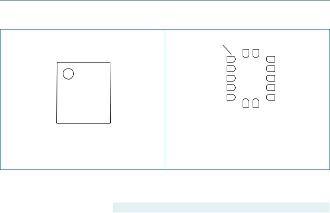
Fig 4. Pin configuration DIP14, SO14 and (T)SSOP14 Fig 5. Pin configuration DHVQFN14
6.2 Pin description
Table 2. |
Pin description |
|
|
|
|
|
|
Symbol |
Pin |
Description |
|
1A to 6A |
1, 3, 5, 9, 11, 13 |
data input 1 |
|
|
|
|
|
1Y to 6Y |
2, 4, 6, 8, 10, 12 |
data output 1 |
|
|
|
|
|
GND |
7 |
ground (0 V) |
|
|
|
|
|
VCC |
14 |
supply voltage |
|
|
|
||
7. Functional description |
|||
Table 3. |
Function table[1] |
|
|
Input |
|
|
Output |
nA |
|
|
nY |
L |
|
|
H |
|
|
|
|
H |
|
|
L |
|
|
|
|
[1]H = HIGH voltage level; L = LOW voltage level.
74HC_HCT14 |
All information provided in this document is subject to legal disclaimers. |
© NXP B.V. 2012. All rights reserved. |
Product data sheet |
Rev. 6 — 19 September 2012 |
3 of 21 |

NXP Semiconductors |
74HC14; 74HCT14 |
|
Hex inverting Schmitt trigger |
8. Limiting values
Table 4. Limiting values
In accordance with the Absolute Maximum Rating System (IEC 60134). Voltages are referenced to GND (ground = 0 V).
Symbol |
Parameter |
Conditions |
|
Min |
Max |
Unit |
VCC |
supply voltage |
|
|
0.5 |
+7 |
V |
IIK |
input clamping current |
VI < 0.5 V or VI > VCC + 0.5 V |
[1] |
- |
20 |
mA |
IOK |
output clamping current |
VO < 0.5 V or VO > VCC + 0.5 V |
[1] |
- |
20 |
mA |
IO |
output current |
0.5 V < VO < VCC + 0.5 V |
|
- |
25 |
mA |
ICC |
supply current |
|
|
- |
50 |
mA |
IGND |
ground current |
|
|
50 |
- |
mA |
Tstg |
storage temperature |
|
|
65 |
+150 |
C |
Ptot |
total power dissipation |
|
[2] |
|
|
|
|
DIP14 package |
|
|
- |
750 |
mW |
|
|
|
|
|
|
|
|
SO14, (T)SSOP14 and |
|
|
- |
500 |
mW |
|
DHVQFN14 packages |
|
|
|
|
|
|
|
|
|
|
|
|
[1]The input and output voltage ratings may be exceeded if the input and output current ratings are observed.
[2]For DIP14 package: Ptot derates linearly with 12 mW/K above 70 C. For SO14 package: Ptot derates linearly with 8 mW/K above 70 C.
For (T)SSOP14 packages: Ptot derates linearly with 5.5 mW/K above 60 C. For DHVQFN14 packages: Ptot derates linearly with 4.5 mW/K above 60 C.
9. Recommended operating conditions
Table 5. |
Recommended operating conditions |
|
|
|
|
|
|
|
||
Voltages are referenced to GND (ground = 0 V) |
|
|
|
|
|
|
|
|||
|
|
|
|
|
|
|
|
|
|
|
Symbol |
Parameter |
Conditions |
|
74HC14 |
|
|
74HCT14 |
|
Unit |
|
|
|
|
Min |
Typ |
Max |
Min |
Typ |
|
Max |
|
VCC |
supply voltage |
2.0 |
5.0 |
6.0 |
4.5 |
5.0 |
|
5.5 |
V |
|
|
|
|
|
|
|
|
|
|
|
|
VI |
input voltage |
0 |
- |
VCC |
0 |
- |
|
VCC |
V |
|
|
|
|
|
|
|
|
|
|
|
|
VO |
output voltage |
0 |
- |
VCC |
0 |
- |
|
VCC |
V |
|
Tamb |
ambient temperature |
|
40 |
+25 |
+125 |
40 |
+25 |
|
+125 |
C |
|
|
|
|
|
|
|
|
|
|
|
74HC_HCT14 |
All information provided in this document is subject to legal disclaimers. |
© NXP B.V. 2012. All rights reserved. |
Product data sheet |
Rev. 6 — 19 September 2012 |
4 of 21 |

NXP Semiconductors |
|
|
|
74HC14; 74HCT14 |
|||||||
|
|
|
|
|
|
|
|
Hex inverting Schmitt trigger |
|||
10. Static characteristics |
|
|
|
|
|
|
|
|
|||
Table 6. |
Static characteristics |
|
|
|
|
|
|
|
|
||
At recommended operating conditions; voltages are referenced to GND (ground = 0 V). |
|
|
|
|
|||||||
|
|
|
|
|
|
|
|
|
|
|
|
Symbol |
|
Parameter |
Conditions |
Tamb = 25 C |
Tamb = 40 C |
Tamb = 40 C |
Unit |
||||
|
|
|
|
|
|
|
to +85 C |
to +125 C |
|
||
|
|
|
|
Min |
Typ |
Max |
Min |
Max |
Min |
Max |
|
74HC14 |
|
|
|
|
|
|
|
|
|
|
|
|
|
|
|
|
|
|
|
|
|
|
|
VOH |
HIGH-level |
VI = VT+ or VT |
|
|
|
|
|
|
|
|
|
|
|
output voltage |
|
|
|
|
|
|
|
|
|
|
|
IO = 20 A; VCC = 2.0 V |
1.9 |
2.0 |
- |
1.9 |
- |
1.9 |
- |
V |
|
|
|
|
|||||||||
|
|
|
IO = 20 A; VCC = 4.5 V |
4.4 |
4.5 |
- |
4.4 |
- |
4.4 |
- |
V |
|
|
|
IO = 20 A; VCC = 6.0 V |
5.9 |
6.0 |
- |
5.9 |
- |
5.9 |
- |
V |
|
|
|
IO = 4.0 mA; VCC = 4.5 V |
3.98 |
4.32 |
- |
3.84 |
- |
3.7 |
- |
V |
|
|
|
IO = 5.2 mA; VCC = 6.0 V |
5.48 |
5.81 |
- |
5.34 |
- |
5.2 |
- |
V |
VOL |
LOW-level |
VI = VT+ or VT |
|
|
|
|
|
|
|
|
|
|
|
output voltage |
|
|
|
|
|
|
|
|
|
|
|
IO = 20 A; VCC = 2.0 V |
- |
0 |
0.1 |
- |
0.1 |
- |
0.1 |
V |
|
|
|
|
|||||||||
|
|
|
IO = 20 A; VCC = 4.5 V |
- |
0 |
0.1 |
- |
0.1 |
- |
0.1 |
V |
|
|
|
IO = 20 A; VCC = 6.0 V |
- |
0 |
0.1 |
- |
0.1 |
- |
0.1 |
V |
|
|
|
IO = 4.0 mA; VCC = 4.5 V |
- |
0.15 |
0.26 |
- |
0.33 |
- |
0.4 |
V |
|
|
|
IO = 5.2 mA; VCC = 6.0 V |
- |
0.16 |
0.26 |
- |
0.33 |
- |
0.4 |
V |
II |
input leakage |
VI = VCC or GND; VCC = 6.0 V |
- |
- |
0.1 |
- |
1.0 |
- |
1.0 |
A |
|
|
|
current |
|
|
|
|
|
|
|
|
|
|
|
|
|
|
|
|
|
|
|
|
|
ICC |
supply current |
VI = VCC or GND; IO = 0 A; |
- |
- |
2.0 |
- |
20 |
- |
40 |
A |
|
|
|
|
VCC = 6.0 V |
|
|
|
|
|
|
|
|
CI |
input |
|
- |
3.5 |
- |
- |
- |
- |
- |
pF |
|
|
|
capacitance |
|
|
|
|
|
|
|
|
|
|
|
|
|
|
|
|
|
|
|
|
|
74HCT14 |
|
|
|
|
|
|
|
|
|
|
|
|
|
|
|
|
|
|
|
|
|
|
|
VOH |
HIGH-level |
VI = VT+ or VT ; VCC = 4.5 V |
|
|
|
|
|
|
|
|
|
|
|
output voltage |
|
|
|
|
|
|
|
|
|
|
|
IO = 20 A |
4.4 |
4.5 |
- |
4.4 |
- |
4.4 |
- |
V |
|
|
|
|
|||||||||
|
|
|
IO = 4.0 mA |
3.98 |
4.32 |
- |
3.84 |
- |
3.7 |
- |
V |
VOL |
LOW-level |
VI = VT+ or VT ; VCC = 4.5 V |
|
|
|
|
|
|
|
|
|
|
|
output voltage |
|
|
|
|
|
|
|
|
|
|
|
IO = 20 A; |
- |
0 |
0.1 |
- |
0.1 |
- |
0.1 |
V |
|
|
|
|
|||||||||
|
|
|
IO = 4.0 mA; |
- |
0.15 |
0.26 |
- |
0.33 |
- |
0.4 |
V |
II |
input leakage |
VI = VCC or GND; VCC = 5.5 V |
- |
- |
0.1 |
- |
1.0 |
- |
1.0 |
A |
|
|
|
current |
|
|
|
|
|
|
|
|
|
|
|
|
|
|
|
|
|
|
|
|
|
ICC |
supply current |
VI = VCC or GND; IO = 0 A; |
- |
- |
2.0 |
- |
20 |
- |
40 |
A |
|
|
|
|
VCC = 5.5 V |
|
|
|
|
|
|
|
|
ICC |
additional |
per input pin; |
- |
30 |
108 |
- |
135 |
- |
147 |
A |
|
|
|
supply current |
VI = VCC 2.1 V; other pins |
|
|
|
|
|
|
|
|
|
|
|
at VCC or GND; IO = 0 A; |
|
|
|
|
|
|
|
|
|
|
|
VCC = 4.5 V to 5.5 V |
|
|
|
|
|
|
|
|
CI |
input |
|
- |
3.5 |
- |
- |
- |
- |
- |
pF |
|
|
|
capacitance |
|
|
|
|
|
|
|
|
|
|
|
|
|
|
|
|
|
|
|
|
|
74HC_HCT14 |
All information provided in this document is subject to legal disclaimers. |
© NXP B.V. 2012. All rights reserved. |
Product data sheet |
Rev. 6 — 19 September 2012 |
5 of 21 |
NXP Semiconductors |
|
|
|
|
74HC14; 74HCT14 |
||||||||
|
|
|
|
|
|
|
|
|
|
Hex inverting Schmitt trigger |
|||
11. Dynamic characteristics |
|
|
|
|
|
|
|
|
|
||||
Table 7. |
Dynamic characteristics |
|
|
|
|
|
|
|
|
|
|||
GND = 0 V; CL = 50 pF; for test circuit see Figure 7. |
|
|
|
|
|
|
|
|
|
||||
Symbol |
|
Parameter |
|
Conditions |
|
|
Tamb = 25 C |
|
Tamb = 40 C to |
Unit |
|||
|
|
|
|
|
|
|
|
|
|
|
+125 C |
|
|
|
|
|
|
|
|
Min |
|
Typ |
|
Max |
Max |
Max |
|
|
|
|
|
|
|
|
|
|
|
|
(85 C) |
(125 C) |
|
74HC14 |
|
|
|
|
|
|
|
|
|
|
|
|
|
|
|
|
|
|
|
|
|
|
|
|
|
|
|
tpd |
propagation delay |
nA to nY; see Figure 6 |
[1] |
|
|
|
|
|
|
|
|
||
|
|
|
|
VCC = 2.0 V |
|
- |
41 |
|
125 |
155 |
190 |
ns |
|
|
|
|
|
VCC = 4.5 V |
|
- |
15 |
|
25 |
31 |
38 |
ns |
|
|
|
|
|
VCC = 5.0 V; CL = 15 pF |
|
- |
12 |
|
- |
- |
- |
ns |
|
|
|
|
|
VCC = 6.0 V |
|
- |
12 |
|
21 |
26 |
32 |
ns |
|
tt |
transition time |
see Figure 6 |
[2] |
|
|
|
|
|
|
|
|
||
|
|
|
|
VCC = 2.0 V |
|
- |
19 |
|
75 |
95 |
110 |
ns |
|
|
|
|
|
VCC = 4.5 V |
|
- |
7 |
|
15 |
19 |
22 |
ns |
|
|
|
|
|
VCC = 6.0 V |
|
- |
6 |
|
13 |
15 |
19 |
ns |
|
CPD |
power dissipation |
per package; VI = GND to VCC |
[3] |
- |
7 |
|
- |
- |
- |
pF |
|||
|
|
capacitance |
|
|
|
|
|
|
|
|
|
|
|
74HCT14 |
|
|
|
|
|
|
|
|
|
|
|
|
|
|
|
|
|
|
|
|
|
|
|
|
|
||
tpd |
propagation delay |
nA to nY; see Figure 6 |
[1] |
|
|
|
|
|
|
|
|
||
|
|
|
|
VCC = 4.5 V |
|
- |
20 |
|
34 |
43 |
51 |
ns |
|
|
|
|
|
VCC = 5.0 V; CL = 15 pF |
|
- |
17 |
|
- |
- |
- |
ns |
|
tt |
transition time |
VCC = 4.5 V; see Figure 6 |
[2] |
- |
7 |
|
15 |
19 |
22 |
ns |
|||
CPD |
power dissipation |
per package; |
[3] |
- |
8 |
|
- |
- |
- |
pF |
|||
|
|
capacitance |
VI = GND to VCC 1.5 V |
|
|
|
|
|
|
|
|
|
|
[1]tpd is the same as tPHL and tPLH.
[2]tt is the same as tTHL and tTLH.
[3]CPD is used to determine the dynamic power dissipation (PD in W): PD = CPD VCC2 fi N + (CL VCC2 fo) where:
fi = input frequency in MHz; fo = output frequency in MHz;
CL = output load capacitance in pF; VCC = supply voltage in V;
N = number of inputs switching;
(CL VCC2 fo) = sum of outputs.
74HC_HCT14 |
All information provided in this document is subject to legal disclaimers. |
© NXP B.V. 2012. All rights reserved. |
Product data sheet |
Rev. 6 — 19 September 2012 |
6 of 21 |
NXP Semiconductors |
74HC14; 74HCT14 |
|
Hex inverting Schmitt trigger |
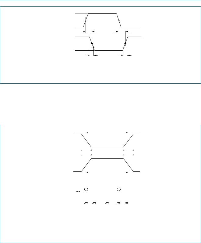
12. Waveforms
VI
nA input
GND
VOH
nY output
VOL
VM |
VM |
tPHL |
tPLH |
90 %
VM VM 10 %
tTHL |
tTLH |
mna722
Measurement points are given in Table 8.
VOL and VOH are typical voltage output levels that occur with the output load.
Fig 6. Input to output propagation delays
Table 8. |
Measurement points |
|
|
|
|
|
|
|
|
|
|
|
|
|
|
|
|
|
|
|
|
|
|
|
|
|
|
|
|
|
|
|
|
|
|
|
|
|
|
|
|
|
|
|
|
|
||
|
|
|
|
|
|
|
|
|
|
|
|
|
|
|
|
|
|
|
|
|
|
|
|
|
|
|
|
|
|
|
|
|
|
|
|
|
|
|
|
|
|
|
|
|
|
|
|
|
Type |
|
Input |
|
|
|
|
Output |
|
|
|
|
|
|
|
|
|
|
|
|
|
|
|
|
|
|
|
|
|
|
|
|
|||||||||||||||||
|
|
VM |
|
|
|
|
VM |
|
|
|
|
|
|
|
VX |
VY |
||||||||||||||||||||||||||||||||
74HC14 |
|
0.5VCC |
|
|
|
|
0.5VCC |
|
|
|
|
|
|
|
0.1VCC |
0.9VCC |
||||||||||||||||||||||||||||||||
74HCT14 |
|
1.3 V |
|
|
|
|
1.3 V |
|
|
|
|
|
|
|
0.1VCC |
0.9VCC |
||||||||||||||||||||||||||||||||
|
|
|
|
|
|
|
|
|
|
|
|
|
|
|
|
|
|
|
|
|
|
|
|
|
|
|
|
|
|
|
|
|
|
|
|
|
|
|
|
|
|
|
|
|
|
|
|
|
|
|
VI |
90 % |
|
|
|
|
|
|
|
|
|
|
|
|
|
|
|
|
|
|
tW |
|
|
|
|
|
|
|
|
|
|
|
|
|
|
|
|
|
|
|
|||||||
|
|
|
|
|
|
|
|
|
|
|
|
|
|
|
|
|
|
|
|
|
|
|
|
|
|
|
|
|
|
|
|
|
|
|
|
|
|
|
|
|
|
|
||||||
|
|
negative |
|
|
|
|
|
|
VM |
|
|
|
|
|
|
|
VM |
|
|
|
|
|
|
|
|
|
|
|
||||||||||||||||||||
|
|
|
|
|
|
|
|
|
|
|
|
|
|
|
|
|
|
|
|
|
|
|
|
|
|
|
|
|
|
|||||||||||||||||||
|
|
pulse |
|
|
|
|
|
|
|
|
|
|
|
|
|
|
|
10 % |
|
|
|
|
|
|
|
|
|
|
|
|
|
|
|
|
|
|
|
|
|
|
|
|
||||||
|
|
GND |
|
|
|
|
|
|
|
|
|
|
|
|
|
|
|
|
|
|
|
|
|
|
|
|
|
|
|
|
tr |
|
|
|
|
|
|
|
||||||||||
|
|
|
|
|
|
|
|
|
|
|
|
|
|
|
|
|
|
|
|
|
|
|
|
|
|
|
|
|
|
|
|
|
|
|
|
|
|
|||||||||||
|
|
|
|
|
|
|
|
|
tf |
|
|
|
|
|
|
|
|
|
|
|
|
|
|
|
|
|
|
|
|
|
|
|
|
|
|
|
|
|
|
|||||||||
|
|
|
|
|
|
|
|
|
|
|
|
|
|
|
|
|
|
|
|
|
|
|
|
|
|
|
|
|
|
|
|
|
|
|
|
|
|
|
|
|
||||||||
|
|
|
|
|
|
|
|
|
|
|
|
|
|
|
|
|
|
|
|
|
|
|||||||||||||||||||||||||||
|
|
|
|
|
|
|
|
|
|
|
|
|
|
|
|
|
|
|
|
|
|
|
|
|
|
|
|
|
|
|
|
|
|
|
|
|
|
|||||||||||
|
|
VI |
|
|
|
|
|
|
|
|
tr |
|
|
|
|
|
|
|
|
|
|
|
|
|
|
|
|
|
|
|
|
|
tf |
|
|
|
|
|
||||||||||
|
|
|
|
|
|
|
|
|
|
|
90 % |
|
|
|
|
|
|
|
|
|
|
|
|
|
|
|
|
|
|
|||||||||||||||||||
|
|
|
|
|
|
|
|
|
|
|
|
|
|
|
|
|
|
|
|
|
|
|
|
|
|
|
|
|
|
|
|
|
|
|
|
|
|
|
|
|
|
|
||||||
|
|
positive |
|
|
|
|
|
|
|
|
|
|
|
|
|
|
|
|
|
|
|
|
|
|
|
|
|
|
|
|
|
|
|
|
|
|
|
|
|
|
|
|||||||
|
|
|
|
|
|
|
|
|
|
|
|
VM |
|
|
|
|
|
|
|
VM |
|
|
|
|
|
|
|
|
|
|
||||||||||||||||||
|
|
|
|
|
|
|
|
|
|
|
|
|
|
|
|
|
|
|
|
|
|
|
|
|
|
|
|
|
||||||||||||||||||||
|
|
pulse |
|
|
|
|
|
|
|
|
|
|
|
|
|
|
|
|
|
|
|
|
|
|
|
|
||||||||||||||||||||||
|
|
GND 10 % |
|
|
|
|
|
|
|
|
|
|
|
|
|
|
|
|
|
|
tW |
|
|
|
|
|
|
|
|
|
|
|
|
|
|
|
|
|
|
|
|
|
||||||
|
|
|
|
|
|
|
|
|
|
|
|
|
|
|
|
|
|
|
|
|
|
|
|
|
|
|
|
|
|
|
|
|
|
|
|
|
|
|
|
|
||||||||
|
|
|
|
|
|
|
|
|
|
|
|
|
|
|
|
|
|
|
|
|
|
|
|
|
|
|
|
|
|
|
|
|
|
|
|
|
|
|
|
|
||||||||
|
|
|
|
|
|
|
|
|
|
|
|
|
|
|
|
|
|
|
|
|
|
|
|
|
|
|
|
|
|
|
|
|
|
|
|
|
|
|
|
|
|
|
|
|
|
|
||
|
|
|
|
|
|
|
|
|
|
|
|
|
|
|
|
|
|
|
|
|
|
|
|
|
VCC |
|
||||||||||||||||||||||
|
|
|
|
|
|
|
|
|
|
VI |
|
|
|
|
|
VO |
|
|||||||||||||||||||||||||||||||
|
|
|
|
|
|
|
|
|
|
|
|
|
|
|
|
|||||||||||||||||||||||||||||||||
|
|
|
|
|
G |
|
|
DUT |
|
|
||||||||||||||||||||||||||||||||||||||
|
|
|
|
|
|
|
|
|
|
|
|
|
|
|
|
|
|
|
|
|
|
|
|
|
|
|
|
|
|
|
|
|
|
|
|
|
|
|
|
|
|
|||||||
|
|
|
|
|
|
|
|
|
|
|
|
|
|
|
|
|
|
|
|
|
|
|
|
RT |
|
|
|
|
|
|
|
|
|
|
|
|
|
|
CL |
|
||||||||
|
|
|
|
|
|
|
|
|
|
|
|
|
|
|
|
|
|
|
|
|
|
|
|
|
|
|
|
|
|
|
|
|
|
|
|
|
|
|
||||||||||
|
|
|
|
|
|
|
|
|
|
|
|
|
|
|
|
|
|
|
|
|
|
|
|
|
|
|
|
|
|
|
|
|
|
|
|
|
|
|
001aah768 |
|
||||||||
|
|
|
|
|
|
|
|
|
|
|
|
|
|
|
|
|
|
|
|
|
|
|
|
|
|
|
|
|
|
|
|
|
|
|
|
|
|
|
|
|||||||||
|
|
|
|
|
|
|
|
|
|
|
|
|
|
|
|
|
|
|
|
|
|
|
|
|
|
|
|
|
|
|
|
|
|
|
|
|
|
|
|
|||||||||
Test data is given in Table 9.
Definitions test circuit:
RT = termination resistance should be equal to output impedance Zo of the pulse generator.
CL = load capacitance including jig and probe capacitance.
Fig 7. Load circuitry for measuring switching times
74HC_HCT14 |
All information provided in this document is subject to legal disclaimers. |
© NXP B.V. 2012. All rights reserved. |
Product data sheet |
Rev. 6 — 19 September 2012 |
7 of 21 |
Loading...