


LPC2131
Table of contents
 Loading...
UM10120
LPC2131/2/4/6/8 User manual
Rev. 02 — 25 July 2006 User manual LPC213x
Document information
Info Content
Keywords LPC2131, LPC2132, LPC2134, LPC2136, LPC2138, LPC2131/01,
LPC2132/01, LPC2134/01, LPC2136/01, LPC2138/01, LPC2000,
LPC213x, LPC213x/01, ARM, ARM7, embedded, 32-bit, microcontroller
Abstract LPC213x and LPC213x/01 User manual

UM10120_2 © Koninklijke Philips Electronics N.V. 2006. All rights reserved.
User manual LPC213x Rev. 02 — 25 July 2006 2 of 292
Contact information
For additional information, please visit: http://www.semiconductors.philips.com
For sales office addresses, please send an email to: sales.addresses@www.semiconductors.philips.com
Philips Semiconductors
UM10120
LPC213x and LPC213x/01 UM
Revision history
Rev Date Description
02 20060725 Updated edition of the User Manual covering both LPC213x and LPC213x/01 devices. For
detailed list of enhancements introduced by LPC213x/01 see Sectio n 1–2 “
Enhancements
introduced with LPC213x/01 devices” on page 3
Other changes applied to Rev 01:
• ECC information in Section 20–6 “Flash content protection mechanism” corrected
• The SSEL signal description corrected for CPHA = 0 and CPHA = 1 (Section 12–2.2
“SPI data transfers”)
• Bit SPIE description corrected in Section 12–4.1 “SPI Control Register (S0SPCR -
0xE002 0000)”
• Details on V
BAT
setup added in Section 18–5 “RTC usage notes”
01 20050624 Initial version

UM10120_2 © Koninklijke Philips Electronics N.V. 2006. All rights reserved.
User manual LPC213x Rev. 02 — 25 July 2006 3 of 292
1. Introduction
The LPC213x and LPC213x/01 microcontrollers are based on a 16/32 bit ARM7TDMI-S
CPU with real-time emulation and embedded trace support that combines the
microcontroller with embedded high speed Flash memory r anging from 32 kB to 512 kB. A
128-bit wide memory interface and a unique accelerator architecture enable 32-bit code
execution at maximum clock rate. For critical code size applications, the alternative 16-bit
Thumb Mode reduces code by more than 30 % with minimal performance penalty.
Due to their tiny size and low power consumption, these microcontrollers are ideal for
applications where miniaturization is a key requirement, such as access control and
point-of-sale. With a wide range of serial communications interfaces and on-chip SRAM
options of 8/16/32 kB, they are very well suited for communication gateways and protocol
converters, soft modems, voice recognition and low end imaging, providing both large
buffer size and high processing power. Various 32-bit timers, single or dual 10-bit
8 channel ADC(s), 10-bit DAC, PWM channels and 47 fast GPIO lines with up to nine
edge or level sensitive external interrupt pins make these microcontrollers particularly
suitable for industrial control and medical systems.
Important: The term “LPC213x“ in the following text will be used both for devices with and
without /01 suffix. Only when needed “LPC213x/01” will be used to identify the latest ones:
LPC2131/01, LPC2132/01, LPC2134/01, LPC2136/01, and/or LPC2138/01.
2. Enhancements introduced with LPC213x/01 devices
• Fast GPIO ports enable pin toggling up to 3.5x faster than the original LPC213x. Also,
Enhanced parallel ports allow for a port pin to be read at any time regardless of the
function selected on it. For details see GPIO chapter on page 78.
• Dedicated result registers for AD converter(s) reduce interrupt overhead. For details
see ADC chapter on page 211.
• UART0/1 include Fractional Baudrate Generator, auto-bauding capabilities and
handshake control fully implemented in hardware. For more details see UART0
chapter on page 92 and UART1 chapter on page 108.
• Enhanced BOD control enables further reduction of power consumption. For det ails
see Table 4–30 “Power Control register (PCON - address 0xE01F C0C0) bit
description” on page 41
3. Features
• 16/32-bit ARM7TDMI-S microcontroller in a tiny LQFP64 package
• 8/16/32 kB of on-chip static RAM and 32/64/128/256/512 kB of on-chip Flash program
memory. 128 bit wide interface/accelerator enables high speed 60 MHz operation.
• In-System/In-Application Programming (ISP/IAP) via on-chip boot-loader software.
Single Flash sector or full chip erase in 400 ms and 256 bytes programming in 1 ms.
UM10120
Chapter 1: Introductory information
Rev. 02 — 25 July 2006 User manual LPC213x

UM10120_2 © Koninklijke Philips Electronics N.V. 2006. All rights reserved.
User manual LPC213x Rev. 02 — 25 July 2006 4 of 292
Philips Semiconductors
UM10120
Chapter 1: Introductory information
• EmbeddedICE and Embedded Trace interfaces offer real-time debugging with the
on-chip RealMonitor software and high speed tracing of instruction execution.
• One (LPC2131/2) or two (LPC2134/6/8) 8 channel 10-bit A/D converters provide a
total of up to 16 analog inputs, with conversion times as low as 2.44 µs per channel.
• Single 10-bit D/A converter provides variable analog output. (LPC2132/4/6/8 only).
• Two 32-bit timers/external event counters (with four capture and four compare
channels each), PWM unit (six outputs) and watchdog.
• Low power Real-time clock with independent power and dedicated 32 kHz clock input.
• Multiple serial interfaces including two UARTs (16C550), two Fast I
2
C (400 kbit/s), SPI
and SSP with buffering and variable data length capabilities.
• Vectored interrupt controller with configurable priorities and vector addresses.
• Up to 47 of 5 V tolerant general purpose I/O pins in a tiny LQFP64 package.
• Up to nine edge or level sensitive external interrupt pins available.
• 60 MHz maximum CPU clock available from programmable on-chip Phase-Locked
Loop (PLL) with settling time of 100 µs.
• On-chip integrated oscillator operates with external crystal from 1 MHz to 25 MHz.
• Power saving modes include Idle and Power-down.
• Individual enable/disable of peripheral functions as well as peripheral clock scaling
down for additional power optimization.
• Processor wake-up from Power-down mode via external interrupt or Real-time Clock.
• Single power supply chip with Power-On Reset (POR) and Brown-Out Detection
(BOD) circuits:
– CPU operating voltage range of 3.0 V to 3.6 V (3.3 V ± 10 %) with 5 V tolerant I/O
pads
4. Applications
• Industrial control
• Medical systems
• General purpose applications
• Communication gateway
• Embedded soft modem
• Access control
• Point-of-sale

UM10120_2 © Koninklijke Philips Electronics N.V. 2006. All rights reserved.
User manual LPC213x Rev. 02 — 25 July 2006 5 of 292
Philips Semiconductors
UM10120
Chapter 1: Introductory information
5. Device information
6. Architectural overview
The LPC213x consists of an ARM7TDMI-S CPU with emulation support, the ARM7 Lo ca l
Bus for interface to on-chip memory controllers, the AMBA Advanced High-performance
Bus (AHB) for interface to the interrupt controller, and the VLSI Peripheral Bus (APB, a
compatible superset of ARM’s AMBA Advanced Peripher al Bus) for connection to on-chip
peripheral functions. The LPC213x configures the ARM7TDMI-S processor in little-endian
byte order.
AHB peripherals are allocated a 2 megabyte range of addresses at the very top of the
4 gigabyte ARM memory space. Each AHB peripheral is allocate d a 16 kB address space
within the AHB address space. LPC213x peripheral functions (other than the interrupt
controller) are connected to the APB bus. The AHB to APB bridge interfaces the APB bus
to the AHB bus. APB peripherals are also allocated a 2 megabyte range of addresses,
beginning at the 3.5 gigabyte address point. Each APB peripheral is allocated a 16 kB
address space within the APB address space.
The connection of on-chip peripherals to device pins is controlled by a Pin Connect Block
(see chapter "Pin Connect Block" on page 72). This must be configured by softwa re to fit
specific application requirements for the use of periph er al functions and pins.
7. ARM7TDMI-S processor
The ARM7TDMI-S is a general purpose 32-bit microprocessor, which offers high
performance and very low power consumption. The ARM architecture is based on
Reduced Instruction Set Computer (RISC) principles, and the instruction set and related
decode mechanism are much simpler than those of microprogrammed Complex
Instruction Set Computers. This simplicity results in a high instruction throughput and
impressive real-time interrupt response from a small and cost-effective processor core.
Table 1. LPC213x and LPC213x/01 device information
Device Pins SRAM FLASH Number of
10-bit ADC
channels
Number of
10-bit DAC
channels
UART1
with
modem
interface
UARTs
with BRG
and
autobaud
UART1
with hw
auto
CTS/RTS
Fast
GPIOs
ADC with
individual
result
registers
LPC2131 64 8 kB 32 kB 8
LPC2131/01 64 8 kB 32 kB 8 + + +
LPC2132 64 16 kB 64 kB 8 1
LPC2132/01 64 16 kB 64 kB 8 1 + + +
LPC2134 64 16 kB 128 kB 16 1 +
LPC2134/01 64 16 kB 128 kB 16 1 + + + + +
LPC2136 64 32 kB 256 kB 16 1 +
LPC2136/01 64 32 kB 256 kB 16 1 + + + + +
LPC2138 64 32 kB 512 kB 16 1 +
LPC2138/01 64 32 kB 512 kB 16 1 + + + + +

UM10120_2 © Koninklijke Philips Electronics N.V. 2006. All rights reserved.
User manual LPC213x Rev. 02 — 25 July 2006 6 of 292
Philips Semiconductors
UM10120
Chapter 1: Introductory information
Pipeline techniques are employed so that all part s of the pro cessing and memory systems
can operate continuously. T ypically, while one instruction is being executed, its successor
is being decoded, and a third instruction is being fetched from memory.
The ARM7TDMI-S processor also employs a unique architectural strategy known as
THUMB, which makes it ideally suited to high-volume applications with memory
restrictions, or applications where code density is an issue.
The key idea behind THUMB is that of a super-reduced instruction set. Essentially, the
ARM7TDMI-S processor has two instruction sets:
• The standard 32-bit ARM instruction set.
• A 16-bit THUMB instruction set.
The THUMB set’s 16-bit instruction length allows it to approach twice the density of
standard ARM code while retaining most of the ARM’s performance advantage over a
traditional 16-bit processor using 16-bit registers. This is possible because THUMB code
operates on the same 32-bit register set as ARM code.
THUMB code is able to provide up to 65% of the code size of ARM, and 160% of the
performance of an equivalent ARM processor connected to a 16-bit memory system.
The ARM7TDMI-S processor is described in detail in the ARM7TDMI-S Datasheet that
can be found on official ARM website.
8. On-chip Flash memory system
The LPC213x incorporates a 32, 64, 128, 256 or 512 kB Flash memory system. This
memory may be used for both code and dat a stor age. Progra mming of the Fl ash memory
may be accomplished in several ways: over the serial builtin JTAG interface, using In
System Programming (ISP) and UART0, or by means of In Application Programming
(IAP) capabilities. The application program, using the IAP functions, may also erase
and/or program the Flash while the application is running, allowing a great degree of
flexibility for data storage field firmware upgrades, etc. When the LPC213x on-chip
bootloader is used, 32/64/128/256/500 kB of Flash memory is available for user code
and/or data storage.
The LPC213x Flash memory provides minimum of 100,000 erase/write cycles and 20
years of data-retention.
9. On-chip Static RAM (SRAM)
On-chip Static RAM (SRAM) may be used for code and/or data storage. The on-chip
SRAM may be accessed as 8-bits, 16-bits, and 32-bits. The LPC213x provide 8/16/32 kB
of static RAM.
The LPC213x SRAM is designed to be accessed as a byte-addressed memory. Word and
halfword accesses to the memory ignore the alignment of the address and access the
naturally-aligned value that is addressed (so a memory access ignores address bits 0 and
1 for word accesses, and ignores bit 0 for halfword accesses). Therefore valid reads and
writes require data accessed as halfwords to originate from addresses with address line 0
being 0 (addresses ending with 0, 2, 4, 6, 8, A, C, and E in hexadecimal nottaion) and

UM10120_2 © Koninklijke Philips Electronics N.V. 2006. All rights reserved.
User manual LPC213x Rev. 02 — 25 July 2006 7 of 292
Philips Semiconductors
UM10120
Chapter 1: Introductory information
data accessed as words to originate from adresses with address lines 0 and 1 being 0
(addresses ending with 0, 4, 8, and C in hexadecimal notation). This rule applies to both
off and on-chip memory usage.
The SRAM controller incorporates a write-back buffer in order to prevent CPU stalls
during back-to-back writes. The write-back buffer always holds the last data sent by
software to the SRAM. This data is only written to the SRAM when another write is
requested by software (the data is only written to the SRAM when software does another
write). If a chip reset occurs, actual SRAM contents will not reflect the most recent write
request (i.e. after a "warm" chip reset, the SRAM does not reflect the last wr ite operation).
Any software that checks SRAM contents after reset must take this into account. Two
identical writes to a location guarantee that the data will be present after a Reset.
Alternatively, a dummy write operation before entering idle or power-down mode will
similarly guarantee that the last data written will be present in SRAM after a subsequent
Reset.
UM10120_2 © Koninklijke Philips Electronics N.V. 2006. All rights reserved.
User manual LPC213x Rev. 02 — 25 July 2006 8 of 292
Philips Semiconductors
UM10120
Chapter 1: Introductory information
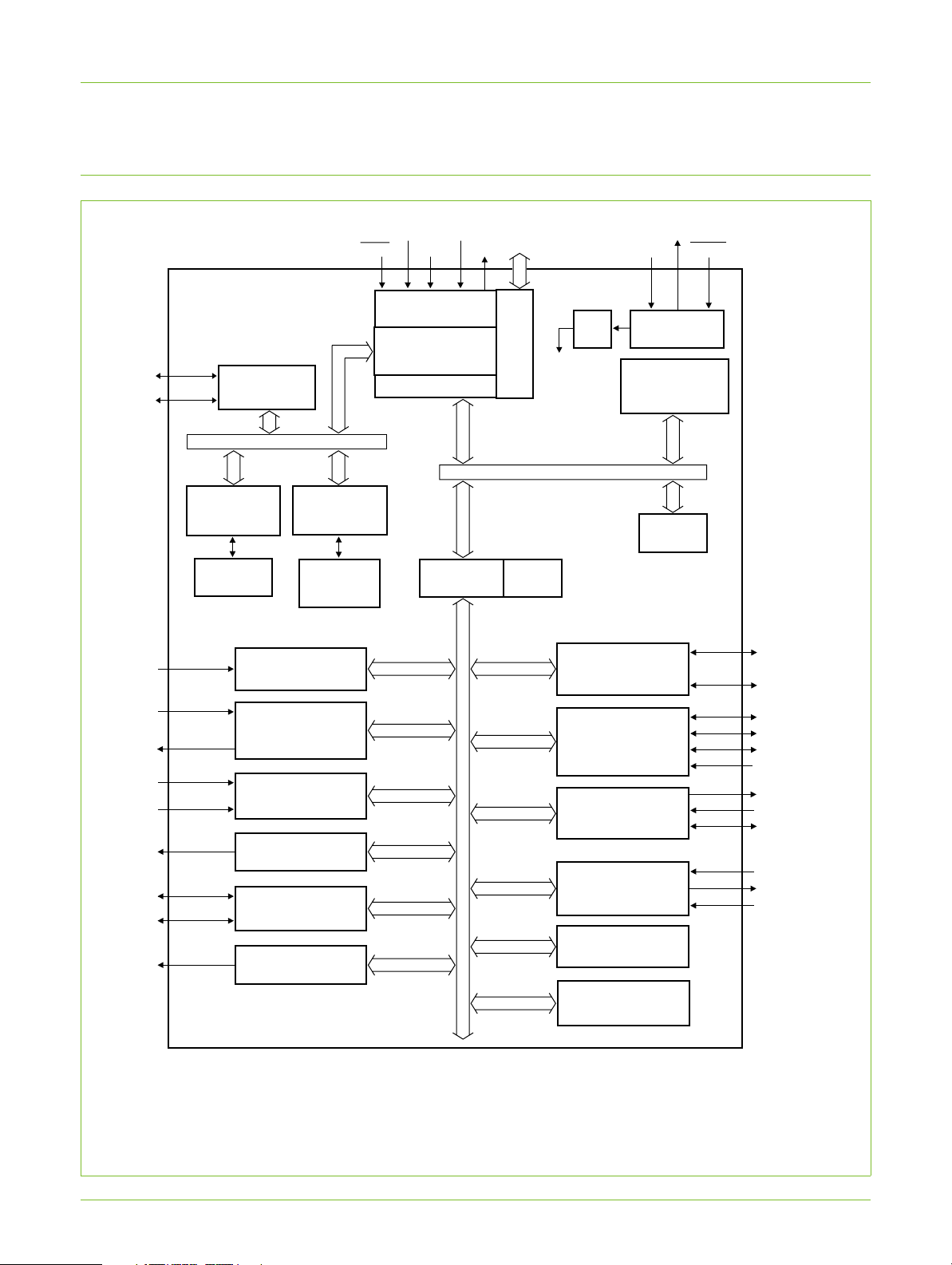
10. Block diagram
(1) Not available on LPC2131 and LPC2131/01.
(2) Not available on LPC2131, LPC2131/01, LPC2132, and LPC2132/01.
(3) Pins shared with GPIO.
Fig 1. LPC213x block diagram.
SCL0,1
P0[31:0]
P1[31:16]
P0[31:0]
P1[31:16]
SDA0,1
XTAL2
XTAL1
SCK0,1
MOSI0,1
MISO0,1
EINT[3:0]
AD0[7:0]
PWM[6:1]
SSEL0,1
TXD0,1
RXD0,1
AHB BRIDGE
PLL
UART0/UART1
REAL TIME CLOCK
PWM0
ARM7TDMI-S
RESET
LPC2131, LPC2131/01
LPC2132, LPC2132/01
LPC2134, LPC2134/01
LPC2136, LPC2136/01
LPC2138, LPC2138/01
8 × CAP
8 × MAT
AD1[7:0]
(1)
AOUT
(2)
DSR1
(1)
,CTS1
(1)
RTS1
(1)
, DTR1
(1)
DCD1
(1)
, RI1
(1)
002aab067
TRST
(3)
TMS
(3)
TCK
(3)
TDI
(3)
TDO
(3)
trace
signals
FAST GENERAL
PURPOSE I/O
INTERNAL
SRAM
CONTROLLER
INTERNAL
FLASH
CONTROLLER
8/16/32 kB
SRAM
32/64/128/
256/512 kB
FLASH
EXTERNAL
INTERRUPTS
CAPTURE/
COMPARE
TIMER 0/TIMER 1
A/D CONVERTERS
0 AND 1
(1)
D/A CONVERTER
(2)
GENERAL
PURPOSE I/O
SYSTEM
CONTROL
WATCHDOG
TIMER
RTCX2
RTCX1
SPI AND SSP
SERIAL INTERFACES
I
2
C SERIAL
INTERFACES 0 AND 1
APB (ARM
peripheral bus)
AHB TO APB
BRIDGE
APB
DIVIDER
AHB
DECODER
AMBA AHB
(Advanced High-performance Bus)
VECTORED
INTERRUPT
CONTROLLER
SYSTEM
FUNCTIONS
system
clock
EMULATION
TRACE MODULE
TEST/DEBUG
INTERFACE
ARM7 local bus
V
BAT

UM10120_2 © Koninklijke Philips Electronics N.V. 2006. All rights reserved.
User manual LPC213x Rev. 02 — 25 July 2006 9 of 292
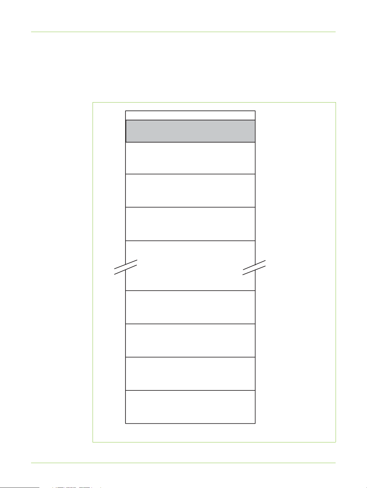
1. Memory maps
The LPC213x incorporates several distinct memory regions, shown in the following
figures. Figure 2–2
shows the overall map of the entire address space from the user
program viewpoint following reset. The interrupt vector area supports address remapping,
which is described later in this section.
UM10120
Chapter 2: Memory maps
Rev. 02 — 25 July 2006 User manual LPC213x
Fig 2. System memory map
TOTAL OF 32 kB ON-CHIP NON-VOLATILE MEMORY
(LPC2131, LPC2131/01)
0xC000 0000
0x8000 0000
0x0000 0000
0.0 GB
1.0 GB
2.0 GB
3.75 GB
4.0 GB
3.0 GB
TOTAL OF 64 kB ON-CHIP NON-VOLATILE MEMORY
(LPC2132, LPC2132/01)
RESERVED ADDRESS SPACE
8 kB ON-CHIP STATIC RAM
(LPC2131, LPC2131/01)
16 kB ON-CHIP STATIC RAM
(LPC2132, LPC2132/01, LPC2134, LPC2134/01)
32 kB ON-CHIP STATIC RAM
(LPC2136, LPC2136/01, LPC2138, LPC2138/01)
RESERVED ADDRESS SPACE
BOOT BLOCK
(12 kB REMAPPED FROM ON-CHIP FLASH MEMORY)
RESERVED ADDRESS SPACE
AHB PERIPHERALS
APB PERIPHERALS
3.5 GB
0x4000 4000
0x4000 3FFF
0x4000 8000
0x4000 7FFF
0x4000 0000
0xE000 0000
0xF000 0000
0xFFFF FFFF
TOTAL OF 128 kB ON-CHIP NON-VOLATILE MEMORY
(LPC2134, LPC2134/01)
TOTAL OF 256 kB ON-CHIP NON-VOLATILE MEMORY
(LPC2136, LPC2136/01)
TOTAL OF 512 kB ON-CHIP NON-VOLATILE MEMORY
(LPC2138, LPC2138/01)
0x4000 2000
0x4000 1FFF
0x0000 8000
0x0000 7FFF
0x0001 0000
0x0000 FFFF
0x0002 0000
0x0001 FFFF
0x0004 0000
0x0003 FFFF
0x0008 0000
0x0007 FFFF
0x7FFF D000

UM10120_2 © Koninklijke Philips Electronics N.V. 2006. All rights reserved.
User manual LPC213x Rev. 02 — 25 July 2006 10 of 292
Philips Semiconductors
UM10120
Chapter 2: Memory maps
Figure 2–3 through Figure 2–4 and Table 2–2 show different views of the peripheral
address space. Both the AHB and APB peripheral areas are 2 megabyte spaces which
are divided up into 128 peripherals. Each peripheral space is 16 kilobytes in size. This
allows simplifying the address decoding for each peripheral. All peripheral register
AHB section is 128 x 16 kB blocks (totaling 2 MB).
APB section is 128 x 16 kB blocks (totaling 2MB).
Fig 3. Peripheral memory map
RESERVED
RESERVED
0xF000 0000
0xEFFF FFFF
APB PERIPHERALS
0xE020 0000
0xE01F FFFF
0xE000 0000
AHB PERIPHERALS
0xFFFF FFFF
0xFFE0 0000
0xFFDF FFFF
3.75 GB
3.5 GB
3.5 GB + 2 MB
4.0 GB - 2 MB
4.0 GB
UM10120_2 © Koninklijke Philips Electronics N.V. 2006. All rights reserved.
User manual LPC213x Rev. 02 — 25 July 2006 11 of 292
Philips Semiconductors
UM10120
Chapter 2: Memory maps
addresses are word aligned (to 32-bit boundaries) regardless of their size. This eliminates
the need for byte lane mapping hardware that would be required to allow byte (8-bit) or
half-word (16-bit) accesses to occur at smaller boundaries. An implication of this is that
word and half-word registers must be accessed all at once. For example, it is not p ossible
to read or write the upper byte of a word register separately.
Fig 4. AHB peripheral map
VECTORED INTERRUPT CONTROLLER
(AHB PERIPHERAL #0)
0xFFFF F000 (4G - 4K)
0xFFFF C000
0xFFFF 8000
(AHB PERIPHERAL #125)
(AHB PERIPHERAL #124)
(AHB PERIPHERAL #3)
(AHB PERIPHERAL #2)
(AHB PERIPHERAL #1)
(AHB PERIPHERAL #126)
0xFFFF 4000
0xFFFF 0000
0xFFE1 0000
0xFFE0 C000
0xFFE0 8000
0xFFE0 4000
0xFFE0 0000

UM10120_2 © Koninklijke Philips Electronics N.V. 2006. All rights reserved.
User manual LPC213x Rev. 02 — 25 July 2006 12 of 292
Philips Semiconductors
UM10120
Chapter 2: Memory maps
2. LPC213x memory re-mapping and boot block
2.1 Memory map concepts and operating modes
The basic concept on the LPC213x is that each memory area has a "natural" location in
the memory map. This is the address range for which code residing in that area is written.
The bulk of each memory space remains permanently fixed in the same location,
eliminating the need to have portions of the code designed to run in different address
ranges.
Because of the location of the interrupt vectors on the ARM7 processor (at addresses
0x0000 0000 through 0x0000 001C, as shown in Table 2–3
below), a small portion of the
Boot Block and SRAM spaces need to be re-mapped in order to allow alternative uses of
interrupts in the different operating modes described in Table 2–4
. Re-mapping of the
interrupts is accomplished via the Memory Mapping Contro l feature (Section 4–7 “
Memory
mapping control” on page 32).
Table 2. APB peripheries and base addresses
APB peripheral Base address Peripheral name
0 0xE000 0000 Watchdog timer
1 0xE000 4000 Timer 0
2 0xE000 8000 Timer 1
3 0xE000 C000 UART0
4 0xE001 0000 UART1
5 0xE001 4000 PWM
6 0xE001 8000 Not used
7 0xE001 C000 I
2
C0
8 0xE002 0000 SPI0
9 0xE002 4000 RTC
10 0xE002 8000 GPIO
11 0xE002 C000 Pin connect block
12 0xE003 0000 Not usef
13 0xE003 4000 10 bit AD0
14-22 0xE003 8000 -
0xE005 8000
Not used
23 0xE005 C000 I
2
C1
24 0xE006 0000 10 bit AD1
25 0xE006 4000 Not used
26 0xE006 8000 SSP
27 0xE006 C000 DAC
28 - 126 0xE007 0000 -
0xE01F 8000
Not used
127 0xE01F C000 System control block

UM10120_2 © Koninklijke Philips Electronics N.V. 2006. All rights reserved.
User manual LPC213x Rev. 02 — 25 July 2006 13 of 292
Philips Semiconductors
UM10120
Chapter 2: Memory maps
2.2 Memory re-mapping
In order to allow for compatibility with future derivatives, the entire Boot Block is mapped
to the top of the on-chip memory space. In this manner, the use of larger or smaller flash
modules will not require changing the location of the Boot Block (which would require
changing the Boot Loader code itself) or changing the mapping of the Boot Block interru pt
vectors. Memory spaces other than the interrupt vectors remain in fixed locations.
Figure 2–5
shows the on-chip memory mapping in the modes defined above.
The portion of memory that is re-mapped to allow interrupt processing in different modes
includes the interrupt vector area (32 bytes) and an additional 32 bytes, for a total of
64 bytes. The re-mapped code locations overlay addresses 0x0000 0000 through
0x0000 003F. A typical user program in the Flash memory can place the entire FIQ
handler at address 0x0000 001C without any need to consider memory boundaries. The
vector contained in the SRAM, external memory, and Boot Block must contain branches to
the actual interrupt handlers, or to other instructions that accomplish the branch to the
interrupt handlers.
There are three reasons this configuration was chosen:
1. To give the FIQ handler in the Flash memory the advantage of not having to take a
memory boundary caused by the remapping into account.
Table 3. ARM exception vector locations
Address Exception
0x0000 0000 Reset
0x0000 0004 Undefined Instruction
0x0000 0008 Software Interrupt
0x0000 000C Prefetch Abort (instruction fetch memory fault)
0x0000 0010 Data Abort (data access memory fault)
0x0000 0014 Reserved
Note: Identified as reserved in ARM documentation, this location is used
by the Boot Loader as the Valid User Program key. This is descibed in
detail in "Flash Memory System and Programming" chapter on page 237.
0x0000 0018 IRQ
0x0000 001C FIQ
Table 4. LPC213x memory mapping modes
Mode Activation Usage
Boot
Loader
mode
Hardware
activation by
any Reset
The Boot Loader always executes after any reset. The Boot Block
interrupt vectors are mapped to the bottom of memory to allow
handling exceptions and using interrupts during the Boot Loading
process.
User
Flash
mode
Software
activation by
Boot code
Activated by Boot Loader when a valid User Program Signature is
recognized in memory and Boot Loader operation is not forced.
Interrupt vectors are not re-mapped and are found in the bottom of the
Flash memory.
User RAM
mode
Software
activation by
User program
Activated by a User Program as desired. Interrupt vectors are
re-mapped to the bottom of the Static RAM.

UM10120_2 © Koninklijke Philips Electronics N.V. 2006. All rights reserved.
User manual LPC213x Rev. 02 — 25 July 2006 14 of 292
Philips Semiconductors
UM10120
Chapter 2: Memory maps
2. Minimize the ne ed to for the SRAM and Boot Block vectors to deal with arbitrary
boundaries in the middle of code space.
3. To provide space to store constant s for jumping beyond the range of single word
branch instructions.
Re-mapped memory areas, including the Boot Block and interrupt vectors, continue to
appear in their original location in addition to the re-mapped address.
Details on re-mapping and examples can be found in Section 4–7 “
Memory mapping
control” on page 32.

UM10120_2 © Koninklijke Philips Electronics N.V. 2006. All rights reserved.
User manual LPC213x Rev. 02 — 25 July 2006 15 of 292
Philips Semiconductors
UM10120
Chapter 2: Memory maps
Fig 5. Map of lower memory is showing re-mapped and re-mappable areas (LPC2138 and
LPC2138/01 with 512 kB Flash)
0.0 GB
0x8000 0000
0x4000 0000
0x3FFF FFFF
0x0000 0000
1.0 GB
2.0 GB - 12 kB
2.0 GB
ACTIVE INTERRUPT VECTORS
(FROM FLASH, SRAM, BOOT ROM, OR EXT MEMORY)
12 kB BOOT BLOCK RE-MAPPED TO HIGHER ADDRESS RANGE
RESERVED FOR ON-CHIP MEMORY
(SRAM INTERRUPT VECTORS)
512 kB ON-CHIP NON-VOLATILE MEMORY
RESERVED FOR ON-CHIP MEMORY
(RE-MAPPED FROM ON-CHIP FLASH MEMORY)
12 kB BOOT BLOCK
32 kB ON-CHIP SRAM
0x7FFF FFFF
0x7FFF D000
0x7FFF CFFF
BOOT BLOCK INTERRUPT VECTORS
0x4000 8000
0x4000 7FFF
0x0007 FFFF
0x0008 0000

UM10120_2 © Koninklijke Philips Electronics N.V. 2006. All rights reserved.
User manual LPC213x Rev. 02 — 25 July 2006 16 of 292
Philips Semiconductors
UM10120
Chapter 2: Memory maps
3. Prefetch abort and data abort exceptions
The LPC213x generates the appropriate bus cycle abort exception if an access is
attempted for an address that is in a reserved or unassigned address region. The regions
are:
• Areas of the memory map that are not implemented for a specific ARM derivative. Fo r
the LPC213x, this is:
– Address space between On-Chip Non-Volatile Memory and On-Chip SRAM,
labelled "Reserved Address Space" in Figure 2–2
and Figure 2–5. For 32 kB Flash
device this is memory address range from 0x0000 8000 to 0x3FFF FFFF, for 64 kB
Flash device this is memory address range from 0x0001 0000 to 0x3FFF FFFF, for
128 kB Flash device this is memory address range from 0x0002 0000 to
0x3FFF FFFF, for 256 kB Flash device this is memory address range from
0x0004 0000 to 0x3FFF FFFF while for 512 kB Flash device this range is from
0x0008 0000 to 0x3FFF FFFF.
– Address space between On-Chip Static RAM and the Boot Block. Labelled
"Reserved Address Space" in Figure 2–2
. For 8 kB SRAM device this is memory
address range from 0x4000 2000 to 0x7FFF CFFF, for 16 kB SRAM device this is
memory address range from 0x4000 4000 to 0x7FFF CFFF, while for 32 kB SRAM
device this range is from 0x4000 8000 to 0x7FFF CFFF.
– Address space between 0x8000 0000 and 0xDFFF FFFF, labelled "Reserved
Adress Space".
– Reserved regions of the AHB and APB spaces. See Figure 2–3
.
• Unassigned AHB peripheral spaces. See Figure 2–4.
• Unassigned APB peripheral spaces. See Table 2–2.
For these areas, both attempted data acce ss and in struction fetch genera te an exception.
In addition, a Prefetch Abort exception is generated for any instruction fetch that maps to
an AHB or APB peripheral address.
Within the address space of an existing APB peripheral, a data abort exception is not
generated in response to an access to an undefined address. Address decoding within
each peripheral is limited to that needed to distinguish defined registers within the
peripheral itself. For example, an access to address 0xE000 D000 (an undefined address
within the UART0 space) may result in an access to the register defined at address
0xE000 C000. Details of such address aliasing within a peripheral space are not defined
in the LPC213x documentation and are not a supported feature.
Note that the ARM core stores the Prefetch Abort flag along with the associated
instruction (which will be meaningless) in the pipeline and processes the abort only if an
attempt is made to execute the instruction fetched from the illegal address. This prevents
accidental aborts that could be caused by prefetches that occur when code is executed
very near a memory boundary.

UM10120_2 © Koninklijke Philips Electronics N.V. 2006. All rights reserved.
User manual LPC213x Rev. 02 — 12 July 2006 17 of 292
1. Introduction
The MAM block in the LPC213x maximizes the performance of the ARM processor when
it is running code in Flash memory but does so using a single Flash bank.
2. Operation
Simply put, the Memory Accelerator Module (MAM) attempts to have the next ARM
instruction that will be needed in its latches in time to prevent CPU fetch stalls. The
LPC213x uses one bank of Flash memory, compared to the two banks used on
predecessor devices. It includes three 128-bit buffers called the Prefetch Buffer, the
Branch Trail Buf fer and the data b uffer. When an Instruction Fetch is not satisfied by either
the Prefetch or Branch Trail Buffer, nor has a prefetch been initiated for that line, the ARM
is stalled while a fetch is initiated for the 128-bit line. If a prefetch has been initiated but not
yet completed, the ARM is stalled for a shorter time. Unless aborted by a da ta access, a
prefetch is initiated as soon as the Flash has completed the previous access. The
prefetched line is latched by the Flash module, but the MAM does not capture the line in
its prefetch buffer until the ARM core present s the address from which the prefetch has
been made. If the core presents a different address from the one from which the prefetch
has been made, the prefetched line is discarded.
The Prefetch and Branch Trail buffers each include four 32-bit ARM instructions or eight
16-bit Thumb instructions. During sequential code execution, typically the Prefetch Buf fe r
contains the current instruction and the entire Flash line that contains it.
The MAM differentiates betwee n in str uction and data accesses. Code and data acce sse s
use separate 128-bit buffers. 3 of every 4 sequential 32- bit code or data accesses "hit" in
the buffer without requiring a Flash access (7 of 8 sequ ential 16-bit accesses, 15 of eve ry
16 sequential byte accesses). The fourth (eighth, 16th) sequential data access must
access Flash, aborting any prefetch in progress. When a Flash data access is concluded,
any prefetch that had been in progress is re-initiated.
Timing of Flash read operat ions is programmable and is described later in this section.
In this manner , there is no code fetch penalty for sequential instruction execution when the
CPU clock period is greater than or equal to one fourth of the Flash access time. The
average amount of time spent doing program branches is relatively small (less than 25%)
and may be minimized in ARM (rather than Thumb) code through the use of the
conditional execution feature present in all ARM instructions. This conditional execution
may often be used to avoid small forward branches that would otherwise be necessary.
Branches and other program flow changes cause a break in the sequential flow of
instruction fetches described above. The Branch Trail Buffer captures the line to which
such a non-sequential break occurs. If the same branch is taken again, the next
instruction is taken from the Branch Trail Buffer. When a branch outside the contents of
the Prefetch and Branch T rail Buffer is taken, a st all of several clocks is needed to load the
Branch Trail buffer. Subsequently, there will typically be no further instructionfetch delays
until a new and different branch occurs.
UM10120
Chapter 3: Memory Acceleration Module (MAM)
Rev. 02 — 12 July 2006 User manual LPC213x
UM10120_2 © Koninklijke Philips Electronics N.V. 2006. All rights reserved.
User manual LPC213x Rev. 02 — 12 July 2006 18 of 292
Philips Semiconductors
UM10120
Chapter 3: MAM Module
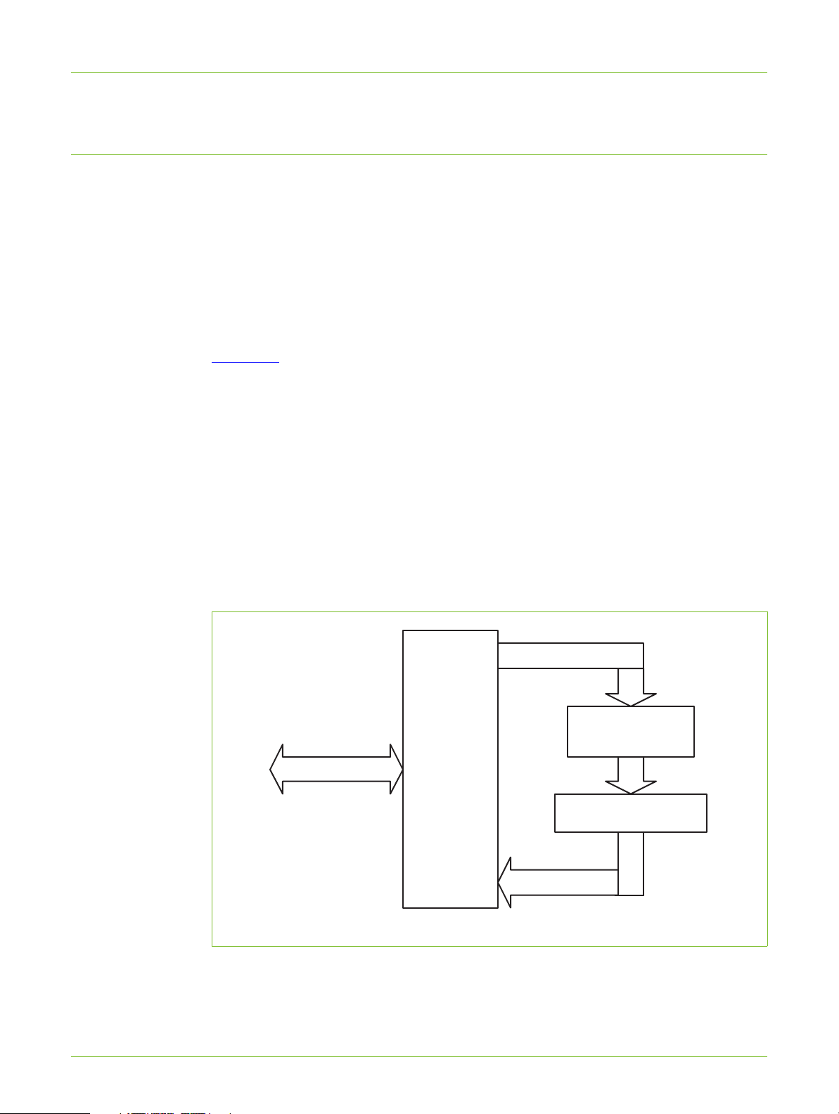
3. MAM blocks
The Memory Accelerator Module is divided into several functional blocks:
• A Flash Address Latch and an incrementor function to form prefetch addresses
• A 128-bit Prefetch Buffer and an associated Address latch and comparator
• A 128-bit Branch Trail Buffer and an associated Address latch and comparator
• A 128-bit Data Buffer and an associated Address latch and comparator
• Control logic
• Wait logic
Figure 3–6
shows a simplified block diagram of the Memory Accelerator Module dat a
paths.
In the following descriptions, the term “fetch” applies to an explicit Flash read request from
the ARM. “Pre-fetch” is used to denote a Flash read of instructions beyond the current
processor fetch address.
3.1 Flash memory bank
There is one bank of Flash memory with the LPC213x MAM.
Flash programming operations are not controlled by the MAM, but are handled as a
separate function. A “boot block” sector contains Flash programming algorithms that may
be called as part of the application program, and a loader that may be run to allow serial
programming of the Flash memory.
3.2 Instruction latches and data latches
Code and Data accesses are treated separately by the Memory Accelerator Module.
There is a 128-bit Latch, a 15-bit Address
Fig 6. Simplified block diagram of the Memory Accelerator Module (MAM)
BUS
INTERFACE
BUFFERS
MEMORY ADDRESS
ARM LOCAL BUS
FLASH MEMORY BANK

UM10120_2 © Koninklijke Philips Electronics N.V. 2006. All rights reserved.
User manual LPC213x Rev. 02 — 12 July 2006 19 of 292
Philips Semiconductors
UM10120
Chapter 3: MAM Module
Latch, and a 15-bit comparator associated with each buffer (prefetch, branch trail, and
data). Each 128-bit latch holds 4 words (4 ARM instructions, or 8 Thumb instructions).
Also associated with each buffer are 32 4:1 Multiplexers that select the requested word
from the 128-bit line.
Each Data access that is not in the Data latch causes a Flash fetch of 4 words of data,
which are captured in the Data latch. This speeds up sequential Data operations, but has
little or no effect on random accesses.
3.3 Flash programming issues
Since the Flash memory does not allow accesses during programming and erase
operations, it is necessary for the MAM to force the CPU to wait if a memory access to a
Flash address is requested while the Flash module is busy. (This is accomplished by
asserting the ARM7TDMI-S local bus signal CLKEN.) Under some conditions, this delay
could result in a Watchdog time-out. The user will need to be aware of this possibility and
take steps to insure that an unwanted Watchdog reset does not cause a system failure
while programming or erasing the Flash memory.
In order to preclude the possibility of stale data being read from the Flash memory, the
LPC213x MAM holding latches are automatically invalidated at the beginnin g of any Flash
programming or erase operation. Any subsequent read from a Flash address will cause a
new fetch to be initiated after the Flash operation has completed.
4. MAM operating modes
Three modes of operation are defined for the MAM, trading off performance for ease of
predictability:
Mode 0: MAM off. All memory requests result in a Flash read operation (see note 2
below). There are no instruction prefetches.
Mode 1: MAM partially enabled. Sequential instruction accesses are fulfilled from the
holding latches if the data is present. Instruction prefetch is enabled. Non-sequential
instruction accesses initiate Flash read operations (see note 2 below). This means that
all branches cause memory fetches. All data operations cause a Flash read because
buffered data access timing is hard to predict and is very situation dependent.
Mode 2: MAM fully enabled. Any memory request (code or data) for a value that is
contained in one of the corresponding holding latches is fulfilled from the latch.
Instruction prefetch is enabled. Flash read operations are initiated for instruction
prefetch and code or data values not available in the corresponding holding latches.
T able 5. MAM responses to program accesses of various types
Program Memory Request Type MAM Mode
0 1 2
Sequential access, data in latches Initiate Fetch
[2]
Use Latched
Data
[1]
Use Latched
Data
[1]
Sequential access, data not in latches Initiate Fetch Initiate Fetch
[1]
Initiate Fetch
[1]
Non-sequential access, data in latches Initiate Fetch
[2]
Initiate Fetch
[1][2]
Use Latched
Data
[1]
Non-sequential access, data not in latches Initiate Fetch Initiate Fetch
[1]
Initiate Fetch
[1]

UM10120_2 © Koninklijke Philips Electronics N.V. 2006. All rights reserved.
User manual LPC213x Rev. 02 — 12 July 2006 20 of 292
Philips Semiconductors
UM10120
Chapter 3: MAM Module
[1] Instruction prefetch is enabled in modes 1 and 2.
[2] The MAM actually uses latched data if it is available, but mimics the timing of a Flash read operation. This
saves power while resulting in the same execution timing. The MAM can truly be turned off by setting the
fetch timing value in MAMTIM to one clock.
[1] The MAM actually uses latched data if it is available, but mimics the timing of a Flash read operation. This
saves power while resulting in the same execution timing. The MAM can truly be turned off by setting the
fetch timing value in MAMTIM to one clock.
5. MAM configuration
After reset the MAM defaults to the disabled state. Software can turn memory access
acceleration on or off at any time. This allows most of an application to be run at the
highest possible performance, while certain functions can be run at a somewhat slower
but more predictable rate if more precise timing is required.
6. Register description
All registers, regardless of size, are on word address boundaries. Details of the registers
appear in the description of each function.
[1] Reset value reflects the data stored in used bits only. It does not include reserved bits content.
7. MAM Control Register (MAMCR - 0xE01F C000)
Two configuration bits select the three MAM operating modes, as shown in Table 3–8.
Following Reset, MAM functions are disabled. Changing the MAM operating mode causes
the MAM to invalidate all of the holding latches, resulting in new reads of Flash
information as required.
T able 6. MAM responses to data and DMA accesses of various types
Data Memory Request T ype MAM Mode
0 1 2
Sequential access, data in latches Initiate Fetch
[1]
Initiate Fetch
[1]
Use Latched
Data
Sequential access, data not in latches Initiate Fetch Initiate Fetch Initiate Fetch
Non-sequential access, data in latches Initiate Fetch
[1]
Initiate Fetch
[1]
Use Latched
Data
Non-sequential access, data not in latches Initiate Fetch Initiate Fetch Initiate Fetch
T able 7. Summary of MAM registers
Name Description Access Reset
value
[1]
Address
MAMCR Memory Accelerator Module Control Register.
Determines the MAM functional mode, that is, to
what extent the MAM performance enhancements
are enabled. See Table 3–8.
R/W 0x0 0xE01F C000
MAMTIM Memory Accelerator Module Timing control.
Determines the number of clocks used for Flash
memory fetches (1 to 7 processor clocks).
R/W 0x07 0xE01F C004

UM10120_2 © Koninklijke Philips Electronics N.V. 2006. All rights reserved.
User manual LPC213x Rev. 02 — 12 July 2006 21 of 292
Philips Semiconductors
UM10120
Chapter 3: MAM Module
8. MAM Timing register (MAMTIM - 0xE01F C004)
The MAM Timing register determines how many CCLK cycles are used to access the
Flash memory. This allows tuning MAM timing to match the processor operating
frequency. Flash access times from 1 clock to 7 clocks are po ssib le . Sing le cloc k Fla sh
accesses would essentially remove the MAM from timing calculations. In this case the
MAM mode may be selected to optimize power usage.
9. MAM usage notes
When changing MAM timing, the MAM must first be turned off by writing a zero to
MAMCR. A new value may then be written to MAMTIM. Finally, the MAM may be turned
on again by writing a value (1 or 2) corresponding to the desired operating mode to
MAMCR.
For system clock slower than 20 MHz, MAMTIM can be 001. For system clock between
20 MHz and 40 MHz, Flash access time is suggested to be 2 CCLKs, while in systems
with system clock faster than 40 MHz, 3 CCLKs are proposed.
T able 8. MAM Control Register (MAMCR - address 0xE01F C000) bit description
Bit Symbol Value Description Reset
value
1:0 MAM_mode
_control
00 MAM functions disabled 0
01 MAM functions partially enabled
10 MAM functions fully en abled
11 Reserved. Not to be used in the application.
7:2 - - Reserved, user software should not write ones to reserved
bits. The value read from a reserved bit is not defined.
NA
T able 9. MAM Timing register (MAMTIM - address 0xE01F C004) bit description
Bit Symbol Value Description Reset
value
2:0 MAM_fetch_
cycle_timing
000 0 - Reserved. 07
001 1 - MAM fetch cycles are 1 processor clock (CCLK) in
duration
010 2 - MAM fetch cycles are 2 CCLKs in duration
011 3 - MAM fetch cycles are 3 CCLKs in duration
100 4 - MAM fetch cycles are 4 CCLKs in duration
101 5 - MAM fetch cycles are 5 CCLKs in duration
110 6 - MAM fetch cycles are 6 CCLKs in duration
111 7 - MAM fetch cycles are 7 CCLKs in duration
Warning: These bits set the duration of MAM Flash fetch operations
as listed here. Improper setting of this value may result in incorrect
operation of the device.
7:3 - - Reserved, user software should not write ones to reserved
bits. The value read from a reserved bit is not defined.
NA

UM10120_2 © Koninklijke Philips Electronics N.V. 2006. All rights reserved.
User manual LPC213x Rev. 02 — 25 July 2006 22 of 292
1. Summary of system control block functions
The System Control Block includes several system features and control registers for a
number of functions that are not related to specific peripheral devices. These include:
• Crystal Oscillator
• External Interrupt Inputs
• Miscellaneous System Controls and Status
• Memory Mapping Control
• PLL
• Power Control
• Reset
• APB Divider
• Wakeup Timer
Each type of function has its own register(s) if any are required and unneeded bits are
defined as reserved in order to allow future expansion. Unrelated functions never share
the same register addresses
2. Pin description
Table 4–10 shows pins that are associated with System Control block functions.
UM10120
Chapter 4: System control block
Rev. 02 — 25 July 2006 User manual LPC213x
Table 10. Pin summary
Pin name Pin
direction
Pin description
XTAL1 Input Crystal Oscillator Input - Input to the oscillator and internal clock
generator circuits
XTAL2 Output Crystal Oscillator Output - Output from the oscillator amplifier
EINT0 Input External Interrupt Input 0 - An active low/high leve l or
falling/rising edge general purpose interrupt input. This pin may be
used to wake up the processor from Idle or Power-down modes.
Pins P0.1 and P0.16 can be selected to perform EINT0 function.
EINT1 Input External Interrupt Input 1 - See the EINT0 descri ption above.
Pins P0.3 and P0.14 can be selected to perform EINT1 function.
Important: LOW level on pin P0.14 immediately after reset is
considered as an external hardware request to start the ISP
command handler. More details on ISP and Serial Boot Loader can
be found in "Flash Memory System and Programming" chapter on
page 237.

UM10120_2 © Koninklijke Philips Electronics N.V. 2006. All rights reserved.
User manual LPC213x Rev. 02 — 25 July 2006 23 of 292
Philips Semiconductors
UM10120
Chapter 4: System control block
3. Register description
All registers, regardless of size, are on word address boundaries. Details of the registers
appear in the description of each function.
[1] Reset value relects the data stored in used bits only. It does not include reserved bits content.
[2] Available in LPC213x/01devices only.
EINT2 Input External Interrupt Input 2 - See the EINT0 descri ption above.
Pins P0.7 and P0.15 can be selected to perform EINT2 function.
EINT3 Input External Interrupt Input 3 - See the EINT0 descri ption above.
Pins P0.9, P0.20 and P0.30 can be selected to perform EINT3
function.
RESET
Input External Reset input - A LOW on this pin resets the chip, causing
I/O ports and peripherals to take on their default states, and the
processor to begin execution at address 0x0000 0000.
Table 10. Pin summary
Pin name Pin
direction
Pin description
T able 11. Summary of system control registers
Name Description Access Reset
value
[1]
Address
External Interrupts
EXTINT External Interrupt Flag Register R/W 0 0xE01F C140
INTWAKE External Interrupt Wakeup Register R/W 0 0xE01F C144
EXTMODE External Interrupt Flag register R/W 0 0xE01F C148
EXTPOLAR External Interrupt Wakeup Register R/W 0 0xE01F C14C
Memory Mapping Control
MEMMAP Memory Mapping Control R/W 0 0xE01F C040
Phase Locked Loop
PLLCON PLL Control Register R/W 0 0xE01F C080
PLLCFG PLL Configuration Register R/W 0 0xE01F C084
PLLSTAT PLL Status Register RO 0 0xE01F C088
PLLFEED PLL Feed Register WO NA 0xE01F C08C
Power Control
PCON Power Control Register R/W 0 0xE01F C0C0
PCONP Power Control for Peripherals R/W 0x03BE 0xE01 F C0C4
APB Divider
APBDIV APB Divider Control R/W 0 0xE01F C100
Reset
RSID Reset Source Identification Register R/W 0 0xE01F C180
Code Security/Debugging
CSPR Code Security Protection Register RO o 0xE01F C184
Syscon Miscellaneous Registers
[2]
SCS System Controls and Status R/W 0 0xE01F C1A0
UM10120_2 © Koninklijke Philips Electronics N.V. 2006. All rights reserved.
User manual LPC213x Rev. 02 — 25 July 2006 24 of 292
Philips Semiconductors
UM10120
Chapter 4: System control block
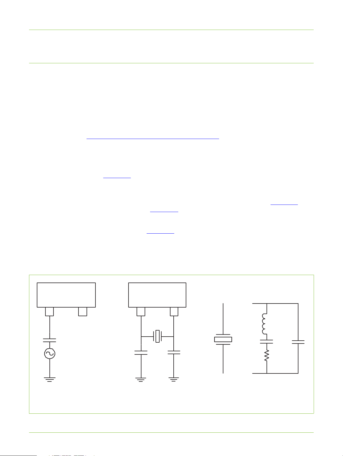
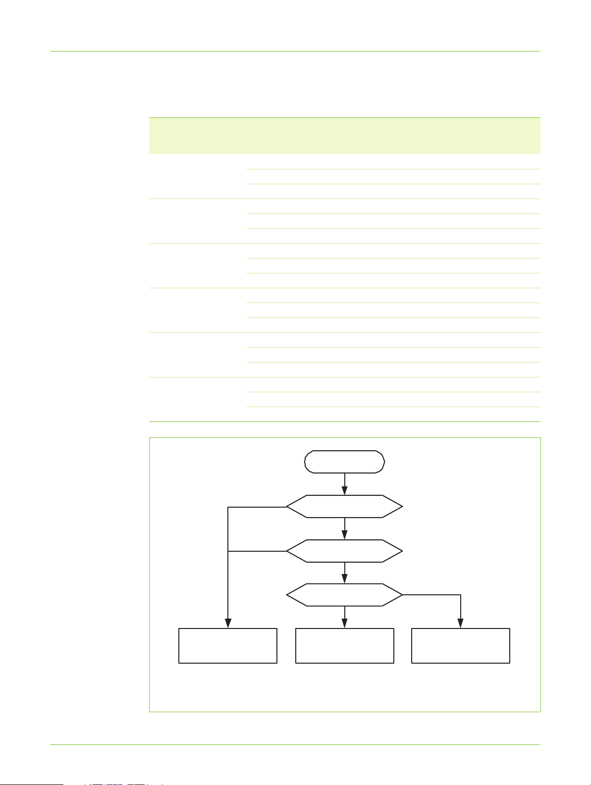
4. Crystal oscillator
While an input signal of 50-50 duty cycle within a frequency range from 1 MHz to 50 MHz
can be used by the LPC213x if supplied to its input XTAL1 pin, this microcontroller’s
onboard oscillator circuit supports external crystals in the range of 1 MHz to 30 MHz only.
If the on-chip PLL system or the boot-loader is used, the input clock frequency is limited to
an exclusive range of 10 MHz to 25 MHz.
The oscillator output frequency is called F
OSC
and the ARM processor clock frequency is
referred to as CCLK for purposes of rate equations, etc. elsewhere in this document. F
OSC
and CCLK are the same value unless the PLL is running and connected. Refer to the
Section 4–8 “
Phase Locked Loop (PLL)” on page 33 for details and frequency limitations.
The onboard oscillator in the LPC213x can operate in one of two modes: slave mode and
oscillation mode.
In slave mode the input clock signal should be coupled by means of a capacitor of 100 pF
(C
C
in Figure 4–7, drawing a), with an amplitude of at least 200 mVrms. The X2 pin in this
configuration can be left not connected. If slave mode is selected, the F
OSC
signal of
50-50 duty cycle can range from 1 MHz to 50 MHz.
External components and models used in oscillation mode are shown in Figure 4–7
,
drawings b and c, and in Table 4–12
. Since the feedback resistance is integrated on chip,
only a crystal and the capacitances C
X1
and C
X2
need to be connected externally in case
of fundamental mode oscillation (the fundamental frequency is represented by L, C
L
and
R
S
). Capacitance C
P
in Figure 4–7, drawing c, represents the parallel package
capacitance and should not be larger than 7 pF. Parameters F
C
, C
L
, R
S
and C
P
are
supplied by the crystal manufacturer.
Choosing an oscillation mode as an on-board oscillator mode of operation limits F
OSC
clock selection to 1 MHz to 30 MHz.
Fig 7. Oscillator modes and models: a) slave mode of operation, b) oscillation mode of operation, c) external
crystal model used for C
X1
/
X2
evaluation
LPC213x LPC213x
Clock
C
C
C
X1
C
X2
C
L
C
P
L
R
S
< = >
a) b) c)
Xtal
XTAL1 XTAL2
XTAL1 XTAL2
UM10120_2 © Koninklijke Philips Electronics N.V. 2006. All rights reserved.
User manual LPC213x Rev. 02 — 25 July 2006 25 of 292
Philips Semiconductors
UM10120
Chapter 4: System control block
T able 12. Recommended values for C
X1/X2
in oscillation mode (crystal and external
components parameters)
Fundamental
oscillation frequency
F
C
Crystal load
capacitance C
L
Maximum crystal
series resistance R
S
External load
capacitors C
X1
,
CX2
1 MHz - 5 MHz 10 pF NA NA
20 pF NA NA
30 pF < 300 Ω 58 pF, 58 pF
5 MHz - 10 MHz 10 pF < 300 Ω 18 pF, 18 pF
20 pF < 300 Ω 38 pF, 38 pF
30 pF < 300 Ω 58 pF, 58 pF
10 MHz - 15 MHz 10 pF < 300 Ω 18 pF, 18 pF
20 pF < 220 Ω 38 pF, 38 pF
30 pF < 140 Ω 58 pF, 58 pF
15 MHz - 20 MHz 10 pF < 220 Ω 18 pF, 18 pF
20 pF < 140 Ω 38 pF, 38 pF
30 pF < 80 Ω 58 pF, 58 pF
20 MHz - 25 MHz 10 pF < 160 Ω 18 pF, 18 pF
20 pF < 90 Ω 38 pF, 38 pF
30 pF < 50 Ω 58 pF, 58 pF
25 MHz - 30 MHz 10 pF < 130 Ω 18 pF, 18 pF
20 pF < 50 Ω 38 pF, 38 pF
30 pF NA NA
Fig 8. F
OSC
selection algorithm
true
MIN f
OSC
= 10 MHz
MAX f
OSC
= 25 MHz
true
MIN f
OSC
= 1 MHz
MAX f
OSC
= 50 MHz
MIN f
OSC
= 1 MHz
MAX f
OSC
= 30 MHz
mode a and/or b mode a mode b
on-chip PLL used
in application?
ISP used for initial
code download?
external crystal
oscillator used?
true
false
false
false
f
OSC
selection

UM10120_2 © Koninklijke Philips Electronics N.V. 2006. All rights reserved.
User manual LPC213x Rev. 02 — 25 July 2006 26 of 292
Philips Semiconductors
UM10120
Chapter 4: System control block
5. External interrupt inputs
The LPC213x includes four External Interrupt Inputs as selectable pin functions. The
External Interrupt Inputs can optionally be used to wake up the processor from
Power-down mode.
5.1 Register description
The external interrupt function has four registers associated with it. The EXTINT register
contains the interrupt flags, and the EXTWAKEUP register contains bits that enable
individual external interrupts to wake up the microcontroller from Power-down mode. The
EXTMODE and EXTPOLAR registers specify the level and edge sensitivity parameters.
[1] Reset value relects the data stored in used bits only. It does not include reserved bits content.
5.2 External Interrupt Flag register (EXTINT - 0xE01F C140)
When a pin is selected for its external interrupt function, the level or edge on that pin
(selected by its bits in the EXTPOLAR a nd EXTMODE registers) will set its interrupt fla g in
this register. This asserts the corresponding interrupt request to the VIC, which will cause
an interrupt if interrupts from the pin are enabled.
Writing ones to bits EINT0 through EINT3 in EXTINT register clears the corre sp onding
bits. In level-sensitive mode this action is efficacious only when the pin is in its inactive
state.
Once a bit from EINT0 to EINT3 is set and an appropriate code star ts to execute (hand ling
wakeup and/or external interrupt), this bit in EXTINT register must be cleared. Otherwise
the event that was just triggered by activity on the EINT pin will not be recognized in the
future.
Important: whenever a change of externa l interrupt operating mode (i.e. active
level/edge) is performed (including the initialization of an external interrupt), the
corresponding bit in the EXTINT register must be cleared! For details see Section
4–5.4 “External Interrupt Mode register (EXTMODE - 0xE01F C148)” and Section 4–5.5
“External Interrupt Polarity register (EXTPOLAR - 0xE01F C14C)”.
Table 13. External interrupt registers
Name Description Access Reset
value
[1]
Address
EXTINT The External Interrupt Flag Register contains
interrupt flags for EINT0, EINT1, EINT2 and
EINT3. See Table 4–14
.
R/W 0 0xE01F C140
INTWAKE The Interrupt Wakeup Register contains four
enable bits that control whether each external
interrupt will cause the processor to wake up
from Power-down mode. See Table 4–15
.
R/W 0 0xE01F C144
EXTMODE The External Interrupt Mode Register controls
whether each pin is edge- or levelsensitive.
R/W 0 0xE01F C148
EXTPOLAR The External Interrupt Polarity Register controls
which level or edge on each pin will cause an
interrupt.
R/W 0 0xE01F C14C

UM10120_2 © Koninklijke Philips Electronics N.V. 2006. All rights reserved.
User manual LPC213x Rev. 02 — 25 July 2006 27 of 292
Philips Semiconductors
UM10120
Chapter 4: System control block
For example, if a system wakes up from power-down using a low level on external
interrupt 0 pin, its post-wakeup code must reset the EINT0 bit in order to a llow future entry
into the power-down mode. If the EINT0 bit is left set to 1, subsequent attempt(s) to invoke
power-down mode will fail. The same goes for external interrupt handling.
More details on power-down mode will be discussed in the following chapters.
Table 14. External Interrupt Flag register (EXTINT - address 0xE01F C140) bit description
Bit Symbol Description Reset
value
0 EINT0 In level-sensitive mode, this bit is set if the EINT0 function is selected for its pin, and the pin is in
its active state. In edge-sensitive mode, this bit is set if the EINT0 function is selected for its pin,
and the selected edge occurs on the pin.
Up to two pins can be selected to perform the EINT0 function (see P0.1 and P0.16 description in
"Pin Configuration" chapter page 64.)
This bit is cleared by writing a one to it, except in level sensitive mode when the pin is in its
active state (e.g. if EINT0 is selected to be low level sensitive and a low level is present on the
corresponding pin, this bit can not be cleared; this bit can be cleared only when the signal on the
pin becomes high).
0
1 EINT1 In level-sensitive mode, this bit is set if the EINT1 function is selected for its pin, and the pin is in
its active state. In edge-sensitive mode, this bit is set if the EINT1 function is selected for its pin,
and the selected edge occurs on the pin.
Up to two pins can be selected to perform the EINT1 function (see P0.3 and P0.14 description in
"Pin Configuration" chapter on page 64.)
This bit is cleared by writing a one to it, except in level sensitive mode when the pin is in its
active state (e.g. if EINT1 is selected to be low level sensitive and a low level is present on the
corresponding pin, this bit can not be cleared; this bit can be cleared only when the signal on the
pin becomes high).
0
2 EINT2 In level-sensitive mode, this bit is set if the EINT2 function is selected for its pin, and the pin is in
its active state. In edge-sensitive mode, this bit is set if the EINT2 function is selected for its pin,
and the selected edge occurs on the pin.
Up to two pins can be selected to perform the EINT2 function (see P0.7 and P0.15 description in
"Pin Configuration" chapter on page 64.)
This bit is cleared by writing a one to it, except in level sensitive mode when the pin is in its
active state (e.g. if EINT2 is selected to be low level sensitive and a low level is present on the
corresponding pin, this bit can not be cleared; this bit can be cleared only when the signal on the
pin becomes high).
0
3 EINT3 In level-sensitive mode, this bit is set if the EINT3 function is selected for its pin, and the pin is in
its active state. In edge-sensitive mode, this bit is set if the EINT3 function is selected for its pin,
and the selected edge occurs on the pin.
Up to three pins can be selected to perform the EINT3 function (see P0.9, P0.20 and P0.30
description in "Pin Configuration" chapter on page 64.)
This bit is cleared by writing a one to it, except in level sensitive mode when the pin is in its
active state (e.g. if EINT3 is selected to be low level sensitive and a low level is present on the
corresponding pin, this bit can not be cleared; this bit can be cleared only when the signal on the
pin becomes high).
0
7:4 - Reserved, user software should not write ones to reserved bits. The value read from a reserved
bit is not defined.
NA

UM10120_2 © Koninklijke Philips Electronics N.V. 2006. All rights reserved.
User manual LPC213x Rev. 02 — 25 July 2006 28 of 292
Philips Semiconductors
UM10120
Chapter 4: System control block
5.3 Interrupt Wakeup register (INTWAKE - 0xE01F C144)
Enable bits in the INTWAKE register allow the external interrupts to wake up the
processor if it is in Power-down mode. The related EINTn function must be mapped to the
pin in order for the wakeup process to take place. It is not necessary for the interrupt to be
enabled in the V ectored Interr upt Controller for a wake up to t ake place. T his arra ngement
allows additional capabilities, such as having an external interrupt input wake up the
processor from Power-down mode without causing an interrupt (simply resuming
operation), or allowing an interrupt to be enabled during Power-down without waking the
processor up if it is asserted (eliminating the need to disable the interrupt if the wakeup
feature is not desirable in the application).
For an external interrupt pin to be a source that would wake up the microco ntroller from
Power-down mode, it is also necessary to clear the corresponding bit in the External
Interrupt Flag register (Section 4–5.2 on page 26
).
5.4 External Interrupt Mode register (EXTMODE - 0xE01F C148)
The bits in this register select whether each EI NT pin is le vel- or edge- sensitive. Only pins
that are selected for the EINT function (see chapter Pin Connect Block on page 72) and
enabled via the VICIntEnable register (Section 5–4.4 “Interrupt Enable register
(VICIntEnable - 0xFFFF F010)” on page 53) can cause interrupts from the External
Interrupt function (though of course pins selected for other functions may cause i nterrupt s
from those functions).
Note: Software should only change a bit in this register when its interrupt is
disabled in the VICIntEnable register, and should write the corresponding 1 to the
EXTINT register before enabling (initializing) or re-enabling the interrupt, to clear
the EXTINT bit that could be set by changing the mode.
Table 15. Interrupt Wakeup register (INTWAKE - address 0xE01F C144) bit desc ription
Bit Symbol Description Reset
value
0 EXTWAKE0 When one, assertion of EINT0 will wake up the processor from
Power-down mode.
0
1 EXTWAKE1 When one, assertion of EINT1 will wake up the processor from
Power-down mode.
0
2 EXTWAKE2 When one, assertion of EINT2 will wake up the processor from
Power-down mode.
0
3 EXTWAKE3 When one, assertion of EINT3 will wake up the processor from
Power-down mode.
0
13:4 - Reserved, user software should not write ones to reserved bits.
The value read from a reserved bit is not defined.
NA
14 BODWAKE When one, a BOD interrupt will wake up the processor from
Power-down mode.
0
15 RTCWAKE When one, assertion of an RTC interrupt will wake up the
processor from Power-down mode.
0

UM10120_2 © Koninklijke Philips Electronics N.V. 2006. All rights reserved.
User manual LPC213x Rev. 02 — 25 July 2006 29 of 292
Philips Semiconductors
UM10120
Chapter 4: System control block
5.5 External Interrupt Polarity register (EXTPOLAR - 0xE01F C14C)
In level-sensitive mode, the bits in this register select whether the corresponding pin is
high- or low-active. In edge-sensitive mode, they select whether the pin is rising- or
falling-edge sensitive. Only pins that are selected for the EINT function (see "Pin Connect
Block" chapter on page 72) and enabled in the VICIntEnable register (Section 5–4.4
“Interrupt Enable register (VICIntEnable - 0xFFFF F010)” on page 53) can cause
interrupts from the External Interrupt function (though of course pins selected for other
functions may cause interrupts from those functions).
Note: Software should only change a bit in this register when its interrupt is
disabled in the VICIntEnable register, and should write the corresponding 1 to the
EXTINT register before enabling (initializing) or re-enabling the interrupt, to clear
the EXTINT bit that could be set by changing the polarity.
Table 16. External Interrupt Mode register (EXTMODE - address 0xE01F C148) bit
description
Bit Symbol Value Description Reset
value
0 EXTMODE0 0 Level-sensitivity is selected for EINT0. 0
1 EINT0 is edge sensitive.
1 EXTMODE1 0 Level-sensitivity is selected for EINT1. 0
1 EINT1 is edge sensitive.
2 EXTMODE2 0 Level-sensitivity is selected for EINT2. 0
1 EINT2 is edge sensitive.
3 EXTMODE3 0 Level-sensitivity is selected for EINT3. 0
1 EINT3 is edge sensitive.
7:4 - - Reserved, user software should not write ones to reserved
bits. The value read from a reserved bit is not defined.
NA
Table 17. External Interrupt Polarity register (EXTPOLAR - address 0xE01F C14C) bit
description
Bit Symbol Value Description Reset
value
0 EXTPOLAR0 0 EINT0 is low-active or falling-edge sensitive (depending on
EXTMODE0 selection).
0
1 EINT0 is high-active or rising-edge sensitive (depending on
EXTMODE0 selection).
1 EXTPOLAR1 0 EINT1 is low-active or falling-edge sensitive (depending on
EXTMODE1 selection).
0
1 EINT1 is high-active or rising-edge sensitive (depending on
EXTMODE1 selection).
2 EXTPOLAR2 0 EINT2 is low-active or falling-edge sensitive (depending on
EXTMODE2 selection).
0
1 EINT2 is high-active or rising-edge sensitive (depending on
EXTMODE2 selection).

UM10120_2 © Koninklijke Philips Electronics N.V. 2006. All rights reserved.
User manual LPC213x Rev. 02 — 25 July 2006 30 of 292
Philips Semiconductors
UM10120
Chapter 4: System control block
5.6 Multiple external interrupt pins
Software can select multiple pins for each of EINT3:0 in the Pin Select registers, which
are described in chapter Pin Connect Block on page 72. The external interrupt logic for
each of EINT3:0 receives the state of all of its associated pins from the pins’ receivers,
along with signals that indicate whether each pin is selected for the EINT function. The
external interrupt logic handles the case when m ore than one pin is so selected, dif ferently
according to the state of its Mode and Polarity bits:
• In Low-Active Level Sensitive mode, the states of all pins selected for the same EINTx
functionality are digitally combined using a positive logic AND gate.
• In High-Active Level Sensitive mode, the states of all pins selected for the same
EINTx functionality are digitally combined using a positive logic OR gate.
• In Edge Sensitive mode, regardless of polarity, the pin with the lowest GPIO port
number is used. (Selecting multiple pins for an EINTx in edge-sensitive mode could
be considered a programming error.)
The signal derived by this logic is the EINTi signal in the following logic schematic
Figure 4–9
.
For example, if the EINT3 function is selected in the PINSEL0 and PINSEL1 registers for
pins P0.9, P0.20 and P0.30, and EINT3 is configured to be low level sensitive, the inputs
from all three pins will be logically ANDed. When more than one EINT pin is logically
ORed, the interrupt service routine can read the states of the pins from the GPIO port
using the IO0PIN and IO1PIN registers, to determine which pin(s) caused the interrupt.
3 EXTPOLAR3 0 EINT3 is low-active or falling-edge sensitive (depending on
EXTMODE3 selection).
0
1 EINT3 is high-active or rising-edge sensitive (depending on
EXTMODE3 selection).
7:4 - - Reserved, user software should not write ones to reserved
bits. The value read from a reserved bit is not defined.
NA
Table 17. External Interrupt Polarity register (EXTPOLAR - address 0xE01F C14C) bit
description
Bit Symbol Value Description Reset
value
Loading...