


Motorola XPC860TZP80nn, XPC860TZP66nn, XPC860TZP50nn, XPC860TCZP66nn, XPC860ENZP50nn Datasheet
...Hardware Specification
MPC860EC/D
Rev. 6.1, 11/2002
MPC860 Family
Hardware Specifications
This document contains detailed information on power considerations, DC/AC electrical characteristics, and AC timing specifications for the MPC860 family.
This document contains the following topics:
Topic |
Page |
Part I, “Overview” |
1 |
Part II, “Features” |
2 |
Part III, “Maximum Tolerated Ratings” |
6 |
Part IV, “Thermal Characteristics” |
7 |
Part V, “Power Dissipation” |
8 |
Part VI, “DC Characteristics” |
9 |
Part VII, “Thermal Calculation and Measurement” |
10 |
Part VIII, “Layout Practices” |
13 |
Part IX, “Bus Signal Timing” |
13 |
Part X, “IEEE 1149.1 Electrical Specifications” |
41 |
Part XI, “CPM Electrical Characteristics” |
43 |
Part XII, “UTOPIA AC Electrical Specifications” |
65 |
Part XIII, “FEC Electrical Characteristics” |
66 |
Part XIV, “Mechanical Data and Ordering Information” |
70 |
Part XV, “Document Revision History” |
74 |
Part I Overview
The MPC860 Quad Integrated Communications Controller (PowerQUICC™) is a versatile one-chip integrated microprocessor and peripheral combination designed for a variety of controller applications. It particularly excels in both communications and networking systems. The PowerQUICC unit is referred to as the MPC860 in this manual.
The MPC860 is a derivative of Motorola’s MC68360 Quad Integrated Communications Controller (QUICC™), referred to here as the QUICC, that implements the PowerPC architecture. The CPU on the MPC860 is a 32-bit

Features
MPC8xx core that incorporates memory management units (MMUs) and instruction and data caches and that implements the PowePC instruction set. The communications processor module (CPM) from the MC68360 QUICC has been enhanced by the addition of the inter-integrated controller (I2C) channel. The memory controller has been enhanced, enabling the MPC860 to support any type of memory, including high-performance memories and new types of DRAMs. A PCMCIA socket controller supports up to two sockets. A real-time clock has also been integrated.
Table 1 shows the functionality supported by the members of the MPC860 family.
Table 1. MPC860 Family Functionality
|
Cache (Kbytes) |
Ethernet |
|
|
|
|||
Part |
|
|
|
|
ATM |
SCC |
Ref. 1 |
|
Instruction |
Data Cache |
10T |
10/100 |
|||||
|
|
|
|
|||||
|
Cache |
|
|
|
||||
|
|
|
|
|
|
|
||
|
|
|
|
|
|
|
|
|
MPC860DE |
4 |
4 |
Up to 2 |
— |
— |
2 |
1 |
|
|
|
|
|
|
|
|
|
|
MPC860DT |
4 |
4 |
Up to 2 |
1 |
yes |
2 |
1,2,3 |
|
|
|
|
|
|
|
|
|
|
MPC860DP |
16 |
8 |
Up to 2 |
1 |
yes |
2 |
1,2,3 |
|
|
|
|
|
|
|
|
|
|
MPC860EN |
4 |
4 |
Up to 4 |
— |
— |
4 |
1 |
|
|
|
|
|
|
|
|
|
|
MPC860SR |
4 |
4 |
Up to 4 |
— |
yes |
4 |
1,2 |
|
|
|
|
|
|
|
|
|
|
MPC860T |
4 |
4 |
Up to 4 |
1 |
yes |
4 |
1,2,3 |
|
|
|
|
|
|
|
|
|
|
MPC860P |
16 |
8 |
Up to 4 |
1 |
yes |
4 |
1,2,3 |
|
|
|
|
|
|
|
|
|
|
MPC855T |
4 |
4 |
1 |
1 |
yes |
1 |
4 |
|
|
|
|
|
|
|
|
|
|
1Supporting documentation for these devices refers to the following:
1.MPC860 PowerQUICC User’s Manual (MPC860UM/D, Rev. 1).
2.MPC8XX ATM Supplement (MPC860SARUM/AD).
3.MPC860T (Rev. D), Fast Ethernet Controller Supplement (MPC860TREVDSUPP).
4.MPC855T User’s Manual (MPC855TUM/D, Rev. 1).
Part II Features
The following list summarizes the key MPC860 features:
•Embedded single-issue, 32-bit MPC8xx core (implementing the PowerPC architecture) with thirty-two 32-bit general-purpose registers (GPRs)
—The core performs branch prediction with conditional prefetch, without conditional execution
—4- or 8-Kbyte data cache and 4- or 16-Kbyte instruction cache (see Table 1)
–16-Kbyte instruction caches are four-way, set-associative with 256 sets; 4-Kbyte instruction caches are two-way, set-associative with 128 sets.
–8-Kbyte data caches are two-way, set-associative with 256 sets; 4-Kbyte data caches are two-way, set-associative with 128 sets.
–Cache coherency for both instruction and data caches is maintained on 128-bit (4-word) cache blocks.
2 |
MPC860 Family Hardware Specifications |
MOTOROLA |

Features
–Caches are physically addressed, implement a least recently used (LRU) replacement algorithm, and are lockable on a cache block basis.
—Instruction and data caches are two-way, set-associative, physically addressed, LRU replacement, and lockable on-line granularity.
—MMUs with 32-entry TLB, fully associative instruction, and data TLBs
—MMUs support multiple page sizes of 4, 16, and 512 Kbytes, and 8 Mbytes; 16 virtual address spaces and 16 protection groups
—Advanced on-chip-emulation debug mode
•Up to 32-bit data bus (dynamic bus sizing for 8, 16, and 32 bits)
•32 address lines
•Operates at up to 80 MHz
•Memory controller (eight banks)
—Contains complete dynamic RAM (DRAM) controller
—Each bank can be a chip select or RAS to support a DRAM bank
—Up to 15 wait states programmable per memory bank
—Glueless interface to DRAM, SIMMS, SRAM, EPROM, Flash EPROM, and other memory devices.
—DRAM controller programmable to support most size and speed memory interfaces
—Four CAS lines, four WE lines, one OE line
—Boot chip-select available at reset (options for 8-, 16-, or 32-bit memory)
—Variable block sizes (32 Kbyte to 256 Mbyte)
—Selectable write protection
—On-chip bus arbitration logic
•General-purpose timers
—Four 16-bit timers or two 32-bit timers
—Gate mode can enable/disable counting
—Interrupt can be masked on reference match and event capture
•System integration unit (SIU)
—Bus monitor
—Software watchdog
—Periodic interrupt timer (PIT)
—Low-power stop mode
—Clock synthesizer
MOTOROLA |
MPC860 Family Hardware Specifications |
3 |

Features
—Decrementer, time base, and real-time clock (RTC) from the PowerPC architecture
—Reset controller
—IEEE 1149.1 test access port (JTAG)
•Interrupts
—Seven external interrupt request (IRQ) lines
—12 port pins with interrupt capability
—23 internal interrupt sources
—Programmable priority between SCCs
—Programmable highest priority request
•10/100 Mbps Ethernet support, fully compliant with the IEEE 802.3u Standard (not available when using ATM over UTOPIA interface)
•ATM support compliant with ATM forum UNI 4.0 specification
—Cell processing up to 50–70 Mbps at 50-MHz system clock
—Cell multiplexing/demultiplexing
—Support of AAL5 and AAL0 protocols on a per-VC basis. AAL0 support enables OAM and software implementation of other protocols).
—ATM pace control (APC) scheduler, providing direct support for constant bit rate (CBR) and unspecified bit rate (UBR) and providing control mechanisms enabling software support of available bit rate (ABR)
—Physical interface support for UTOPIA (10/100-Mbps is not supported with this interface) and byte-aligned serial (for example, T1/E1/ADSL)
—UTOPIA-mode ATM supports level-1 master with cell-level handshake, multi-PHY (up to 4 physical layer devices), connection to 25-, 51-, or 155-Mbps framers, and UTOPIA/system clock ratios of 1/2 or 1/3.
—Serial-mode ATM connection supports transmission convergence (TC) function for T1/E1/ADSL lines; cell delineation; cell payload scrambling/descrambling; automatic idle/unassigned cell insertion/stripping; header error control (HEC) generation, checking, and statistics.
•Communications processor module (CPM)
—RISC communications processor (CP)
—Communication-specific commands (for example, GRACEFUL STOP TRANSMIT,
ENTER HUNT MODE, and RESTART TRANSMIT)
—Supports continuous mode transmission and reception on all serial channels
—Up to 8Kbytes of dual-port RAM
—16 serial DMA (SDMA) channels
4 |
MPC860 Family Hardware Specifications |
MOTOROLA |

Features
—Three parallel I/O registers with open-drain capability
•Four baud-rate generators (BRGs)
—Independent (can be connected to any SCC or SMC)
—Allow changes during operation
—Autobaud support option
•Four serial communications controllers (SCCs)
—Ethernet/IEEE 802.3 optional on SCC1–4, supporting full 10-Mbps operation (available only on specially programmed devices).
—HDLC/SDLC (all channels supported at 2 Mbps)
—HDLC bus (implements an HDLC-based local area network (LAN))
—Asynchronous HDLC to support PPP (point-to-point protocol)
—AppleTalk
—Universal asynchronous receiver transmitter (UART)
—Synchronous UART
—Serial infrared (IrDA)
—Binary synchronous communication (BISYNC)
—Totally transparent (bit streams)
—Totally transparent (frame based with optional cyclic redundancy check (CRC))
•Two SMCs (serial management channels)
—UART
—Transparent
—General circuit interface (GCI) controller
—Can be connected to the time-division multiplexed (TDM) channels
•One SPI (serial peripheral interface)
—Supports master and slave modes
—Supports multimaster operation on the same bus
•One I2C (inter-integrated circuit) port
—Supports master and slave modes
—Multiple-master environment support
•Time-slot assigner (TSA)
—Allows SCCs and SMCs to run in multiplexed and/or non-multiplexed operation
—Supports T1, CEPT, PCM highway, ISDN basic rate, ISDN primary rate, user defined
—1- or 8-bit resolution
MOTOROLA |
MPC860 Family Hardware Specifications |
5 |

Maximum Tolerated Ratings
—Allows independent transmit and receive routing, frame synchronization, clocking
—Allows dynamic changes
—Can be internally connected to six serial channels (four SCCs and two SMCs)
•Parallel interface port (PIP)
—Centronics interface support
—Supports fast connection between compatible ports on the MPC860 or the MC68360
•PCMCIA interface
—Master (socket) interface, release 2.1 compliant
—Supports two independent PCMCIA sockets
—Eight memory or I/O windows supported
•Low power support
—Full on—all units fully powered
—Doze—core functional units disabled, except time base decrementer, PLL, memory controller, RTC, and CPM in low-power standby
—Sleep—all units disabled, except RTC and PIT, PLL active for fast wake up
—Deep sleep—all units disabled including PLL, except RTC and PIT
—Power down mode— all units powered down, except PLL, RTC, PIT, time base, and decrementer
•Debug interface
—Eight comparators: four operate on instruction address, two operate on data address, and two operate on data
—Supports conditions: = ≠ < >
—Each watchpoint can generate a break-point internally
•3.3 V operation with 5-V TTL compatibility except EXTAL and EXTCLK
•357-pin ball grid array (BGA) package
Part III Maximum Tolerated Ratings
This section provides the maximum tolerated voltage and temperature ranges for the MPC860. Table 3-2 provides the maximum ratings.
This device contains circuitry protecting against damage due to high-static voltage or electrical fields; however, it is advised that normal precautions be taken to avoid application of any voltages higher than maximum-rated voltages to this high-impedance circuit. Reliability of operation is enhanced, if unused inputs are tied to an appropriate logic voltage level (for example, either GND or Vdd).
6 |
MPC860 Family Hardware Specifications |
MOTOROLA |

Thermal Characteristics
Table 3-2. Maximum Tolerated Ratings
(GND = 0 V)
Rating |
Symbol |
Value |
Unit |
|
|
|
|
Supply Voltage 1 |
VDDH |
–0.3 to 4.0 |
V |
|
VDDL |
–0.3 to 4.0 |
V |
|
KAPWR |
–0.3 to 4.0 |
V |
|
|
|
|
|
VDDSYN |
–0.3 to 4.0 |
V |
|
|
|
|
Input Voltage 2 |
Vin |
GND – 0.3 to VDDH |
V |
Temperature 3 (Standard) |
T |
0 |
˚C |
|
A(min) |
|
|
|
Tj(max) |
95 |
˚C |
Temperature 3 (Extended) |
T |
–40 |
˚C |
|
A(min) |
|
|
|
Tj(max) |
95 |
˚C |
Storage Temperature Range |
Tstg |
–55 to 150 |
˚C |
1The power supply of the device must start its ramp from 0.0 V.
2Functional operating conditions are provided with the DC electrical specifications in Table 6-5. Absolute maximum ratings are stress ratings only; functional operation at the maxima is not guaranteed. Stress beyond those listed may affect device reliability or cause permanent damage to the device.
Caution: All inputs that tolerate 5 V cannot be more than 2.5 V greater than the supply voltage.This restriction applies to power-up and normal operation (that is, if the MPC860 is unpowered, voltage greater than 2.5 V must not be applied to its inputs).
3Minimum temperatures are guaranteed as ambient temperature, TA. Maximum temperatures are guaranteed as junction temperature, Tj.
Part IV Thermal Characteristics
Table 4-3 shows the thermal characteristics for the MPC860.
Table 4-3. MPC860 Thermal Resistance Data
Rating |
Environment |
Symbol |
Rev A |
Rev |
Unit |
|||
B, C, D |
||||||||
|
|
|
|
|
|
|
||
|
|
|
|
|
|
|
|
|
Junction to Ambient 1 |
Natural Convection |
Single layer board (1s) |
R |
2 |
31 |
40 |
°C/W |
|
|
|
|
|
θJA |
|
|
|
|
|
|
Four layer board (2s2p) |
|
3 |
20 |
25 |
|
|
|
|
RθJMA |
|
|||||
|
Air Flow (200 ft/min) |
Single layer board (1s) |
|
3 |
26 |
32 |
|
|
|
RθJMA |
|
||||||
|
|
Four layer board (2s2p) |
|
3 |
16 |
21 |
|
|
|
|
RθJMA |
|
|||||
Junction to Board 4 |
|
|
RθJB |
8 |
15 |
|
||
Junction to Case 5 |
|
|
RθJC |
5 |
7 |
|
||
Junction to Package Top |
Natural Convection |
|
ΨJT |
1 |
2 |
|
||
6 |
|
|
|
|
|
|
|
|
Air Flow (200 ft/min) |
|
|
|
2 |
3 |
|
||
|
|
|
|
|
||||
|
|
|
|
|
|
|
|
|
1Junction temperature is a function of on-chip power dissipation, package thermal resistance, mounting site (board) temperature, ambient temperature, air flow, power dissipation of other components on the board, and board thermal resistance.
MOTOROLA |
MPC860 Family Hardware Specifications |
7 |

Power Dissipation
2Per SEMI G38-87 and JEDEC JESD51-2 with the single layer board horizontal.
3Per JEDEC JESD51-6 with the board horizontal.
4Thermal resistance between the die and the printed circuit board per JEDEC JESD51-8. Board temperature is measured on the top surface of the board near the package.
5Indicates the average thermal resistance between the die and the case top surface as measured by the cold plate method (MIL SPEC-883 Method 1012.1) with the cold plate temperature used for the case temperature. For exposed pad packages where the pad would be expected to be soldered, junction to case thermal resistance is a simulated value from the junction to the exposed pad without contact resistance.
6Thermal characterization parameter indicating the temperature difference between package top and the junction temperature per JEDEC JESD51-2.
Part V Power Dissipation
Table 5-4 provides power dissipation information. The modes are 1:1, where CPU and bus speeds are equal, and 2:1 mode, where CPU frequency is twice bus speed.
Table 5-4. Power Dissipation (PD)
Die Revision |
Frequency (MHz) |
Typical 1 |
Maximum 2 |
Unit |
|
|
|
|
|
|
|
A.3 and Previous |
25 |
450 |
550 |
mW |
|
|
|
|
|
|
|
|
40 |
700 |
850 |
mW |
|
|
|
|
|
|
|
|
50 |
870 |
1050 |
mW |
|
|
|
|
|
|
|
B.1 and C.1 |
33 |
375 |
TBD |
mW |
|
|
|
|
|
|
|
|
50 |
575 |
TBD |
mW |
|
|
|
|
|
|
|
|
66 |
750 |
TBD |
mW |
|
|
|
|
|
|
|
D.3 and D.4 |
50 |
656 |
735 |
mW |
|
(1:1 Mode) |
|
|
|
|
|
66 |
TBD |
TBD |
mW |
||
|
|||||
|
|
|
|
|
|
D.3 and D.4 |
66 |
722 |
762 |
mW |
|
(2:1 Mode) |
|
|
|
|
|
80 |
851 |
909 |
mW |
||
|
|||||
|
|
|
|
|
1Typical power dissipation is measured at 3.3 V.
2Maximum power dissipation is measured at 3.5 V.
NOTE
Values in Table 5-4” represent VDDL-based power dissipation and do not include I/O power dissipation over VDDH. I/O power dissipation varies widely by application due to buffer current, depending on external circuitry.
8 |
MPC860 Family Hardware Specifications |
MOTOROLA |

DC Characteristics
Part VI DC Characteristics
Table 6-5 provides the DC electrical characteristics for the MPC860.
Table 6-5. DC Electrical Specifications
|
|
|
|
|
Characteristic |
Symbol |
Min |
Max |
Unit |
|||||||||||
|
|
|
|
|
||||||||||||||||
Operating Voltage at 40 MHz or Less |
VDDH, VDDL, VDDSYN |
3.0 |
3.6 |
V |
||||||||||||||||
|
|
|
|
|
|
|
|
|
|
|
|
|
|
|
|
|
KAPWR |
2.0 |
3.6 |
V |
|
|
|
|
|
|
|
|
|
|
|
|
|
|
|
|
|
(power-down mode) |
|
|
|
|
|
|
|
|
|
|
|
|
|
|
|
|
|
|
|
|
|
|
|
|
|
|
|
|
|
|
|
|
|
|
|
|
|
|
|
|
|
KAPWR |
VDDH – 0.4 |
VDDH |
V |
|
|
|
|
|
|
|
|
|
|
|
|
|
|
|
|
|
(all other operating modes) |
|
|
|
|
|
|
|
|
||||||||||||||||
Operating Voltage Greater than 40 MHz |
VDDH, VDDL, KAPWR, |
3.135 |
3.465 |
V |
||||||||||||||||
|
|
|
|
|
|
|
|
|
|
|
|
|
|
|
|
|
VDDSYN |
|
|
|
|
|
|
|
|
|
|
|
|
|
|
|
|
|
|
|
|
|
|
|
|
|
|
|
|
|
|
|
|
|
|
|
|
|
|
|
|
|
KAPWR |
2.0 |
3.6 |
V |
|
|
|
|
|
|
|
|
|
|
|
|
|
|
|
|
|
(power-down mode) |
|
|
|
|
|
|
|
|
|
|
|
|
|
|
|
|
|
|
|
|
|
|
|
|
|
|
|
|
|
|
|
|
|
|
|
|
|
|
|
|
|
KAPWR |
VDDH – 0.4 |
VDDH |
V |
|
|
|
|
|
|
|
|
|
|
|
|
|
|
|
|
|
(all other operating modes) |
|
|
|
|
|
|
|
|
||||||||||||||||
Input High Voltage (All Inputs Except EXTAL |
VIH |
2.0 |
5.5 |
V |
||||||||||||||||
and EXTCLK) |
|
|
|
|
||||||||||||||||
|
|
|
|
|
||||||||||||||||
Input Low Voltage |
VIL |
GND |
0.8 |
V |
||||||||||||||||
EXTAL, EXTCLK Input High Voltage |
VIHC |
0.7 × (VDDH) |
VDDH + 0.3 |
V |
||||||||||||||||
Input Leakage Current, Vin = 5.5 V (Except |
Iin |
— |
100 |
µA |
||||||||||||||||
TMS, |
TRST, |
|
DSCK, and DSDI Pins) |
|
|
|
|
|||||||||||||
|
|
|
|
|
||||||||||||||||
Input Leakage Current, Vin = 3.6 V (Except |
IIn |
— |
10 |
µA |
||||||||||||||||
TMS, |
TRST, |
|
DSCK, and DSDI Pins) |
|
|
|
|
|||||||||||||
|
|
|
|
|
||||||||||||||||
Input Leakage Current, Vin = 0 V (Except |
IIn |
— |
10 |
µA |
||||||||||||||||
TMS, |
TRST, |
|
DSCK, and DSDI Pins) |
|
|
|
|
|||||||||||||
|
|
|
|
|
||||||||||||||||
Input Capacitance 1 |
Cin |
— |
20 |
pF |
||||||||||||||||
Output High Voltage, IOH = –2.0 mA, |
VOH |
2.4 |
— |
V |
||||||||||||||||
VDDH = 3.0 V (Except XTAL, XFC, and Open |
|
|
|
|
||||||||||||||||
Drain Pins) |
|
|
|
|
||||||||||||||||
|
|
|
|
|
||||||||||||||||
Output Low Voltage |
VOL |
— |
0.5 |
V |
||||||||||||||||
IOL = 2.0 mA, CLKOUT |
|
|
|
|
||||||||||||||||
IOL = 3.2 mA 2 |
|
|
|
|
||||||||||||||||
IOL = 5.3 mA 3 |
|
|
|
|
||||||||||||||||
IOL = 7.0 mA, TXD1/PA14, TXD2/PA12 |
|
|
|
|
||||||||||||||||
IOL = 8.9 mA, |
|
|
|
|
|
|
|
|
|
|
|
|
|
|
|
|||||
TS, |
TA, |
TEA, |
BI, |
BB, |
|
|
|
|
||||||||||||
|
HRESET, |
|
SRESET |
|
|
|
|
|
||||||||||||
|
|
|
|
|
||||||||||||||||
1 Input capacitance is periodically sampled. |
|
|
|
|
||||||||||||||||
MOTOROLA |
MPC860 Family Hardware Specifications |
9 |

Thermal Calculation and Measurement
2A(0:31), TSIZ0/REG, TSIZ1, D(0:31), DP(0:3)/IRQ(3:6), RD/WR, BURST, RSV/IRQ2, IP_B(0:1)/IWP(0:1)/ VFLS(0:1), IP_B2/IOIS16_B/AT2, IP_B3/IWP2/VF2, IP_B4/LWP0/VF0, IP_B5/LWP1/VF1, IP_B6/DSDI/AT0, IP_B7/PTR/AT3, RXD1 /PA15, RXD2/PA13, L1TXDB/PA11, L1RXDB/PA10, L1TXDA/PA9, L1RXDA/PA8, TIN1/L1RCLKA/BRGO1/CLK1/PA7, BRGCLK1/TOUT1/CLK2/PA6, TIN2/L1TCLKA/BRGO2/CLK3/PA5, TOUT2/CLK4/PA4, TIN3/BRGO3/CLK5/PA3, BRGCLK2/L1RCLKB/TOUT3/CLK6/PA2, TIN4/BRGO4/CLK7/ PA1, L1TCLKB/TOUT4/CLK8/PA0, REJCT1/SPISEL/PB31, SPICLK/PB30, SPIMOSI/PB29, BRGO4/SPIMISO/
PB28, BRGO1/I2CSDA/PB27, BRGO2/I2CSCL/PB26, SMTXD1/PB25, SMRXD1/PB24, SMSYN1/SDACK1/ PB23, SMSYN2/SDACK2/PB22, SMTXD2/L1CLKOB/PB21, SMRXD2/L1CLKOA/PB20, L1ST1/RTS1/PB19, L1ST2/RTS2/PB18, L1ST3/L1RQB/PB17, L1ST4/L1RQA/PB16, BRGO3/PB15, RSTRT1/PB14, L1ST1/RTS1/ DREQ0/PC15, L1ST2/RTS2/DREQ1/PC14, L1ST3/L1RQB/PC13, L1ST4/L1RQA/PC12, CTS1/PC11, TGATE1/CD1/PC10, CTS2/PC9, TGATE2/CD2/PC8, SDACK2/L1TSYNCB/PC7, L1RSYNCB/PC6, SDACK1/ L1TSYNCA/PC5, L1RSYNCA/PC4, PD15, PD14, PD13, PD12, PD11, PD10, PD9, PD8, PD5, PD6, PD7, PD4, PD3, MII_MDC, MII_TX_ER, MII_EN, MII_MDIO, MII_TXD[0:3].
3BDIP/GPL_B(5), BR, BG, FRZ/IRQ6, CS(0:5), CS(6)/CE(1)_B, CS(7)/CE(2)_B, WE0/BS_B0/IORD, WE1/BS_B1/IOWR, WE2/BS_B2/PCOE, WE3/BS_B3/PCWE, BS_A(0:3), GPL_A0/GPL_B0, OE/GPL_A1/ GPL_B1, GPL_A(2:3)/GPL_B(2:3)/CS(2:3), UPWAITA/GPL_A4, UPWAITB/GPL_B4, GPL_A5, ALE_A, CE1_A, CE2_A, ALE_B/DSCK/AT1, OP(0:1), OP2/MODCK1/STS, OP3/MODCK2/DSDO, BADDR(28:30).
Part VII Thermal Calculation and Measurement
For the following discussions, PD = (VDD × IDD) + PI/O, where PI/O is the power dissipation of the I/O drivers.
7.1Estimation with Junction-to-Ambient Thermal Resistance
An estimation of the chip junction temperature, TJ, in °C can be obtained from the equation: TJ = TA + (RθJA × PD)
where:
TA = ambient temperature (ºC)
RθJA = package junction-to-ambient thermal resistance (ºC/W)
PD = power dissipation in package
The junction-to-ambient thermal resistance is an industry standard value which provides a quick and easy estimation of thermal performance. However, the answer is only an estimate; test cases have demonstrated that errors of a factor of two (in the quantity TJ – TA) are possible.
7.2Estimation with Junction-to-Case Thermal Resistance
Historically, the thermal resistance has frequently been expressed as the sum of a junction-to-case thermal resistance and a case-to-ambient thermal resistance:
RθJA = RθJC + RθCA
10 |
MPC860 Family Hardware Specifications |
MOTOROLA |
Estimation with Junction-to-Board Thermal Resistance
where:
RθJA = junction-to-ambient thermal resistance (ºC/W)
RθJC = junction-to-case thermal resistance (ºC/W)
RθCA = case-to-ambient thermal resistance (ºC/W)
RθJC is device related and cannot be influenced by the user. The user adjusts the thermal environment to affect the case-to-ambient thermal resistance, RθCA. For instance, the user can change the air flow around the device, add a heat sink, change the mounting arrangement on the printed circuit board, or change the thermal dissipation on the printed circuit board surrounding the device. This thermal model is most useful for ceramic packages with heat sinks where some 90% of the heat flows through the case and the heat sink to the ambient environment. For most packages, a better model is required.
7.3Estimation with Junction-to-Board Thermal Resistance
A simple package thermal model which has demonstrated reasonable accuracy (about 20%) is a two resistor model consisting of a junction-to-board and a junction-to-case thermal resistance. The junction-to-case covers the situation where a heat sink is used or where a substantial amount of heat is dissipated from the top of the package. The junction-to-board thermal resistance describes the thermal performance when most of the heat is conducted to the printed circuit board. It has been observed that the thermal performance of most plastic packages and especially PBGA packages is strongly dependent on the board temperature; see Figure 7-1.
Above |
Power |
Power |
|
Above |
Package |
Rise |
Package |
JunctionTemperatureRise |
AmbientDivided byby |
Junction |
Ambient |
1 0 0
9 0
8 0
7 0
6 0
5 0
4 0
3 0
2 0
1 0
0
0 |
2 0 |
4 0 |
6 0 |
8 0 |
Board Temperature Rise Above Ambient Divided by Package Power
Board Temperture Rise Above Ambient Divided by Package
Figure 7-1. Effect of Board Temperature Rise on Thermal Behavior
MOTOROLA |
MPC860 Family Hardware Specifications |
11 |

Estimation Using Simulation
If the board temperature is known, an estimate of the junction temperature in the environment can be made using the following equation:
TJ = TB + (RθJB × PD)
where:
RθJB = junction-to-board thermal resistance (ºC/W)
TB = board temperature (ºC)
PD = power dissipation in package
If the board temperature is known and the heat loss from the package case to the air can be ignored, acceptable predictions of junction temperature can be made. For this method to work, the board and board mounting must be similar to the test board used to determine the junction-to-board thermal resistance, namely a 2s2p (board with a power and a ground plane) and vias attaching the thermal balls to the ground plane.
7.4Estimation Using Simulation
When the board temperature is not known, a thermal simulation of the application is needed. The simple two resistor model can be used with the thermal simulation of the application [2], or a more accurate and complex model of the package can be used in the thermal simulation.
7.5Experimental Determination
To determine the junction temperature of the device in the application after prototypes are available, the thermal characterization parameter (ΨJT) can be used to determine the junction temperature with a measurement of the temperature at the top center of the package case using the following equation:
TJ = TT + (ΨJT × PD)
where:
ΨJT = thermal characterization parameter
TT = thermocouple temperature on top of package PD = power dissipation in package
The thermal characterization parameter is measured per JEDEC JESD51-2 specification using a 40 gauge type T thermocouple epoxied to the top center of the package case. The thermocouple should be positioned so that the thermocouple junction rests on the package. A small amount of epoxy is placed over the thermocouple junction and over about 1 mm of wire extending from the junction. The thermocouple wire is placed flat against the package case to avoid measurement errors caused by cooling effects of the thermocouple wire.
12 |
MPC860 Family Hardware Specifications |
MOTOROLA |

|
|
References |
7.6 |
References |
|
Semiconductor Equipment and Materials International |
(415) 964-5111 |
|
805 East Middlefield Rd |
|
|
Mountain View, CA 94043 |
|
|
MIL-SPEC and EIA/JESD (JEDEC) specifications |
800-854-7179 or |
|
(Available from Global Engineering Documents) |
303-397-7956 |
|
JEDEC Specifications |
http://www.jedec.org |
|
1.1. C.E. Triplett and B. Joiner, “An Experimental Characterization of a 272 PBGA Within an Automotive Engine Controller Module,” Proceedings of SemiTherm, San Diego, 1998, pp. 47–54.
2.2. B. Joiner and V. Adams, “Measurement and Simulation of Junction to Board Thermal Resistance and Its Application in Thermal Modeling,” Proceedings of SemiTherm, San Diego, 1999, pp. 212–220.
Part VIII Layout Practices
Each VDD pin on the MPC860 should be provided with a low-impedance path to the board’s supply. Each GND pin should likewise be provided with a low-impedance path to ground. The power supply pins drive distinct groups of logic on chip. The VDD power supply should be bypassed to ground using at least four 0.1 µF-bypass capacitors located as close as possible to the four sides of the package. The capacitor leads and associated printed circuit traces connecting to chip VDD and GND should be kept to less than half an inch per capacitor lead. A four-layer board is recommended, employing two inner layers as VCC and GND planes.
All output pins on the MPC860 have fast rise and fall times. Printed circuit (PC) trace interconnection length should be minimized in order to minimize undershoot and reflections caused by these fast output switching times. This recommendation particularly applies to the address and data busses. Maximum PC trace lengths of 6 inches are recommended. Capacitance calculations should consider all device loads as well as parasitic capacitances due to the PC traces. Attention to proper PCB layout and bypassing becomes especially critical in systems with higher capacitive loads because these loads create higher transient currents in the VCC and GND circuits. Pull up all unused inputs or signals that will be inputs during reset. Special care should be taken to minimize the noise levels on the PLL supply pins.
Part IX Bus Signal Timing
Table 9-6 provides the bus operation timing for the MPC860 at 33, 40, 50, and 66 MHz.
The maximum bus speed supported by the MPC860 is 66 MHz. Higher-speed parts must be operated in half-speed bus mode (for example, an MPC860 used at 80 MHz must be configured for a 40 MHz bus).
MOTOROLA |
MPC860 Family Hardware Specifications |
13 |
Bus Signal Timing
The timing for the MPC860 bus shown assumes a 50-pF load for maximum delays and a 0-pF load for minimum delays.
Table 9-6. Bus Operation Timings
|
|
|
|
|
|
|
|
|
|
|
|
|
|
|
|
|
|
|
|
|
|
|
|
|
|
|
|
|
|
33 MHz |
40 MHz |
50 MHz |
66 MHz |
|
||||
Num |
|
|
|
|
|
|
|
|
Characteristic |
|
|
|
|
|
|
|
|
Unit |
||||||||||||||||||||
|
|
|
|
|
|
|
|
Min |
Max |
Min |
Max |
Min |
Max |
Min |
Max |
|||||||||||||||||||||||
|
|
|
|
|
|
|
|
|
|
|
|
|
|
|
|
|
|
|
|
|
|
|
|
|
|
|
|
|
|
|
||||||||
|
|
|
|
|
|
|
|
|
|
|
|
|||||||||||||||||||||||||||
B1 |
|
CLKOUT period |
30.30 |
30.30 |
25.00 |
30.30 |
20.00 |
30.30 |
15.15 |
30.30 |
ns |
|||||||||||||||||||||||||||
|
|
|
|
|
|
|
|
|
|
|
|
|||||||||||||||||||||||||||
B1a |
|
EXTCLK to CLKOUT phase skew |
–0.90 |
0.90 |
–0.90 |
0.90 |
–0.90 |
0.90 |
–0.90 |
0.90 |
ns |
|||||||||||||||||||||||||||
|
|
(EXTCLK > 15 MHz and MF <= 2) |
|
|
|
|
|
|
|
|
|
|||||||||||||||||||||||||||
|
|
|
|
|
|
|
|
|
|
|
|
|||||||||||||||||||||||||||
B1b |
|
EXTCLK to CLKOUT phase skew |
–2.30 |
2.30 |
–2.30 |
2.30 |
–2.30 |
2.30 |
–2.30 |
2.30 |
ns |
|||||||||||||||||||||||||||
|
|
(EXTCLK > 10 MHz and MF < 10) |
|
|
|
|
|
|
|
|
|
|||||||||||||||||||||||||||
|
|
|
|
|
|
|
|
|
|
|
|
|||||||||||||||||||||||||||
B1c |
|
CLKOUT phase jitter (EXTCLK > |
–0.60 |
0.60 |
–0.60 |
0.60 |
–0.60 |
0.60 |
–0.60 |
0.60 |
ns |
|||||||||||||||||||||||||||
|
|
15 MHz and MF <= 2) 1 |
|
|
|
|
|
|
|
|
|
|||||||||||||||||||||||||||
B1d |
|
CLKOUT phase jitter1 |
–2.00 |
2.00 |
–2.00 |
2.00 |
–2.00 |
2.00 |
–2.00 |
2.00 |
ns |
|||||||||||||||||||||||||||
B1e |
|
CLKOUT frequency jitter (MF < 10) 1 |
— |
0.50 |
— |
0.50 |
— |
0.50 |
— |
0.50 |
% |
|||||||||||||||||||||||||||
B1f |
|
CLKOUT frequency jitter (10 < MF |
— |
2.00 |
— |
2.00 |
— |
2.00 |
— |
2.00 |
% |
|||||||||||||||||||||||||||
|
|
< 500) 1 |
|
|
|
|
|
|
|
|
|
|
|
|
|
|
|
|
|
|
|
|
|
|
|
|
|
|
|
|
|
|
|
|
||||
B1g |
|
CLKOUT frequency jitter (MF > 500) 1 |
— |
3.00 |
— |
3.00 |
— |
3.00 |
— |
3.00 |
% |
|||||||||||||||||||||||||||
B1h |
|
Frequency jitter on EXTCLK 2 |
— |
0.50 |
— |
0.50 |
— |
0.50 |
— |
0.50 |
% |
|||||||||||||||||||||||||||
B2 |
|
CLKOUT pulse width low |
12.12 |
— |
10.00 |
— |
8.00 |
— |
6.06 |
— |
ns |
|||||||||||||||||||||||||||
|
|
|
|
|
|
|
|
|
|
|
|
|||||||||||||||||||||||||||
B3 |
|
CLKOUT width high |
12.12 |
— |
10.00 |
— |
8.00 |
— |
6.06 |
— |
ns |
|||||||||||||||||||||||||||
|
|
|
|
|
|
|
|
|
|
|
|
|||||||||||||||||||||||||||
B4 |
|
CLKOUT rise time 3 |
— |
4.00 |
— |
4.00 |
— |
4.00 |
— |
4.00 |
ns |
|||||||||||||||||||||||||||
B533 |
|
CLKOUT fall time3 |
— |
4.00 |
— |
4.00 |
— |
4.00 |
— |
4.00 |
ns |
|||||||||||||||||||||||||||
B7 |
|
CLKOUT to A(0:31), BADDR(28:30), |
7.58 |
— |
6.25 |
— |
5.00 |
— |
3.80 |
— |
ns |
|||||||||||||||||||||||||||
|
|
|
|
|
|
|
|
|
|
|
|
|
|
|
|
|
|
|
|
|
|
|
|
|
|
|
|
|
|
|
|
|
|
|
|
|
|
|
|
|
RD/WR, |
|
|
BURST, D(0:31), DP(0:3) |
|
|
|
|
|
|
|
|
|
||||||||||||||||||||||||
|
|
invalid |
|
|
|
|
|
|
|
|
|
|||||||||||||||||||||||||||
|
|
|
|
|
|
|
|
|
|
|
|
|
|
|
|
|
|
|||||||||||||||||||||
B7a |
|
CLKOUT to TSIZ(0:1), |
|
|
|
|
|
|
7.58 |
— |
6.25 |
— |
5.00 |
— |
3.80 |
— |
ns |
|||||||||||||||||||||
REG, |
RSV, |
|||||||||||||||||||||||||||||||||||||
|
|
AT(0:3), |
|
|
|
|
|
PTR invalid |
|
|
|
|
|
|
|
|
|
|||||||||||||||||||||
|
|
BDIP, |
|
|
|
|
|
|
|
|
|
|||||||||||||||||||||||||||
|
|
|
|
|
|
|
|
|
|
|
|
|
|
|
|
|
|
|
|
|
|
|
||||||||||||||||
B7b |
|
CLKOUT to |
|
|
|
|
|
|
|
|
|
|
|
|
FRZ, VFLS(0:1), |
7.58 |
— |
6.25 |
— |
5.00 |
— |
3.80 |
— |
ns |
||||||||||||||
BR, |
BG, |
|||||||||||||||||||||||||||||||||||||
|
|
VF(0:2) IWP(0:2), LWP(0:1), |
STS |
|
|
|
|
|
|
|
|
|
|
|||||||||||||||||||||||||
|
|
invalid 4 |
|
|
|
|
|
|
|
|
|
|||||||||||||||||||||||||||
B8 |
|
CLKOUT to A(0:31), BADDR(28:30) |
7.58 |
14.33 |
6.25 |
13.00 |
5.00 |
11.75 |
3.80 |
10.04 |
ns |
|||||||||||||||||||||||||||
|
|
|
|
|
|
|
|
|
|
|
|
|
|
|
|
|
|
|
|
|
|
|
|
|
|
|
||||||||||||
|
|
RD/WR, |
|
BURST, D(0:31), DP(0:3) |
|
|
|
|
|
|
|
|
|
|||||||||||||||||||||||||
|
|
valid |
|
|
|
|
|
|
|
|
|
|||||||||||||||||||||||||||
|
|
|
|
|
|
|
|
|
|
|
|
|
|
|
|
|||||||||||||||||||||||
B8a |
|
CLKOUT to TSIZ(0:1), |
|
|
|
|
|
7.58 |
14.33 |
6.25 |
13.00 |
5.00 |
11.75 |
3.80 |
10.04 |
ns |
||||||||||||||||||||||
REG, |
RSV, |
|||||||||||||||||||||||||||||||||||||
|
|
AT(0:3) |
BDIP, |
PTR valid |
|
|
|
|
|
|
|
|
|
|||||||||||||||||||||||||
|
|
|
|
|
|
|
|
|
|
|
|
|
|
|
|
|
|
|||||||||||||||||||||
B8b |
|
CLKOUT to |
|
|
|
|
|
|
|
|
|
VFLS(0:1), |
7.58 |
14.33 |
6.25 |
13.00 |
5.00 |
11.75 |
3.80 |
10.04 |
ns |
|||||||||||||||||
BR, |
BG, |
|||||||||||||||||||||||||||||||||||||
|
|
VF(0:2), IWP(0:2), FRZ, LWP(0:1), |
|
|
|
|
|
|
|
|
|
|||||||||||||||||||||||||||
|
|
|
valid 4 |
|
|
|
|
|
|
|
|
|
||||||||||||||||||||||||||
|
|
STS |
|
|
|
|
|
|
|
|
|
|||||||||||||||||||||||||||
B9 |
|
CLKOUT to A(0:31), BADDR(28:30), |
7.58 |
14.33 |
6.25 |
13.00 |
5.00 |
11.75 |
3.80 |
10.04 |
ns |
|||||||||||||||||||||||||||
|
|
|
|
|
|
|
|
|
D(0:31), DP(0:3), |
|
|
|
|
|
|
|
|
|
||||||||||||||||||||
|
|
RD/WR, |
BURST, |
|
|
|
|
|
|
|
|
|
||||||||||||||||||||||||||
|
|
TSIZ(0:1), |
REG, |
|
RSV, |
AT(0:3), PTR |
|
|
|
|
|
|
|
|
|
|||||||||||||||||||||||
|
|
High-Z |
|
|
|
|
|
|
|
|
|
|||||||||||||||||||||||||||
|
|
|
|
|
|
|
|
|
|
|
|
|
|
|
|
|
|
|
|
|
|
|
|
|
|
|
|
|
|
|
|
|
|
|
|
|
|
|
|
|
|
|
|
|
|
|
|
|
|
|
|
|
|
|
|
|
|
|
|
|
|
|
|
|
|
|
|
|
|
|
|
|
|
|
|
|
|
14 |
MPC860 Family Hardware Specifications |
MOTOROLA |

Bus Signal Timing
Table 9-6. Bus Operation Timings (continued)
|
|
|
|
|
|
|
|
|
|
|
|
|
|
|
|
|
|
|
|
|
|
|
|
|
|
|
|
|
|
|
|
|
|
|
|
|
|
|
|
|
|
|
|
|
|
|
|
|
33 MHz |
40 MHz |
50 MHz |
66 MHz |
|
||||
Num |
|
|
|
|
|
|
|
|
|
|
|
|
Characteristic |
|
|
|
|
|
|
|
|
Unit |
|||||||||||||||||||||||||||||||||||
|
|
|
|
|
|
|
|
|
|
|
|
Min |
Max |
Min |
Max |
Min |
Max |
Min |
Max |
||||||||||||||||||||||||||||||||||||||
|
|
|
|
|
|
|
|
|
|
|
|
|
|
|
|
|
|
|
|
|
|
|
|
|
|
|
|
|
|
|
|
|
|
|
|
|
|
|
|
|
|
|
|
|
|
|
|
|
|
||||||||
|
|
|
|
|
|
|
|
|
|
|
|
|
|
|
|
|
|
|
|
|
|
|
|
|
|
|
|||||||||||||||||||||||||||||||
B11 |
|
CLKOUT to |
|
|
|
|
|
|
|
|
|
|
|
|
|
|
assertion |
7.58 |
13.58 |
6.25 |
12.25 |
5.00 |
11.00 |
3.80 |
11.29 |
ns |
|||||||||||||||||||||||||||||||
TS, |
BB |
||||||||||||||||||||||||||||||||||||||||||||||||||||||||
|
|
|
|
|
|
|
|
|
|
|
|
|
|
|
|
|
|
|
|
|
|
|
|
||||||||||||||||||||||||||||||||||
B11a |
|
CLKOUT to |
|
|
|
|
|
|
|
|
|
|
|
|
assertion (when |
2.50 |
9.25 |
2.50 |
9.25 |
2.50 |
9.25 |
2.50 |
9.75 |
ns |
|||||||||||||||||||||||||||||||||
TA, |
BI |
||||||||||||||||||||||||||||||||||||||||||||||||||||||||
|
driven by the memory controller or |
|
|
|
|
|
|
|
|
|
|||||||||||||||||||||||||||||||||||||||||||||||
|
PCMCIA interface) |
|
|
|
|
|
|
|
|
|
|||||||||||||||||||||||||||||||||||||||||||||||
|
|
|
|
|
|
|
|
|
|
|
|
|
|
|
|
|
|
|
|
|
|
|
|||||||||||||||||||||||||||||||||||
B12 |
CLKOUT to |
|
|
|
|
|
|
|
|
|
|
|
|
|
negation |
7.58 |
14.33 |
6.25 |
13.00 |
5.00 |
11.75 |
3.80 |
8.54 |
ns |
|||||||||||||||||||||||||||||||||
TS, |
BB |
||||||||||||||||||||||||||||||||||||||||||||||||||||||||
|
|
|
|
|
|
|
|
|
|
|
|
|
|
|
|
|
|
|
|
|
|
|
|
||||||||||||||||||||||||||||||||||
B12a |
|
CLKOUT to |
|
|
|
|
|
|
|
|
|
|
|
|
negation (when |
2.50 |
11.00 |
2.50 |
11.00 |
2.50 |
11.00 |
2.50 |
9.00 |
ns |
|||||||||||||||||||||||||||||||||
TA, |
BI |
||||||||||||||||||||||||||||||||||||||||||||||||||||||||
|
driven by the memory controller or |
|
|
|
|
|
|
|
|
|
|||||||||||||||||||||||||||||||||||||||||||||||
|
PCMCIA interface) |
|
|
|
|
|
|
|
|
|
|||||||||||||||||||||||||||||||||||||||||||||||
|
|
|
|
|
|
|
|
|
|
|
|
|
|
|
|
|
|
|
|
|
|
|
|||||||||||||||||||||||||||||||||||
B13 |
CLKOUT to |
|
|
|
|
|
|
|
|
|
|
|
|
|
High-Z |
7.58 |
21.58 |
6.25 |
20.25 |
5.00 |
19.00 |
3.80 |
14.04 |
ns |
|||||||||||||||||||||||||||||||||
TS, |
BB |
||||||||||||||||||||||||||||||||||||||||||||||||||||||||
|
|
|
|
|
|
|
|
|
|
|
|
|
|
|
|
|
|
|
|
|
|
|
|
||||||||||||||||||||||||||||||||||
B13a |
|
CLKOUT to |
|
|
|
|
|
|
|
|
|
|
|
|
High-Z (when |
2.50 |
15.00 |
2.50 |
15.00 |
2.50 |
15.00 |
2.50 |
15.00 |
ns |
|||||||||||||||||||||||||||||||||
TA, |
BI |
||||||||||||||||||||||||||||||||||||||||||||||||||||||||
|
driven by the memory controller or |
|
|
|
|
|
|
|
|
|
|||||||||||||||||||||||||||||||||||||||||||||||
|
PCMCIA interface) |
|
|
|
|
|
|
|
|
|
|||||||||||||||||||||||||||||||||||||||||||||||
|
|
|
|
|
|
|
|
|
|
|
|
|
|
|
|
|
|
||||||||||||||||||||||||||||||||||||||||
B14 |
CLKOUT to |
|
|
|
|
|
|
|
|
|
|
assertion |
2.50 |
10.00 |
2.50 |
10.00 |
2.50 |
10.00 |
2.50 |
9.00 |
ns |
||||||||||||||||||||||||||||||||||||
TEA |
|||||||||||||||||||||||||||||||||||||||||||||||||||||||||
|
|
|
|
|
|
|
|
|
|
|
|
|
|
|
|
|
|
|
|||||||||||||||||||||||||||||||||||||||
B15 |
|
CLKOUT to |
|
|
|
|
|
|
|
|
|
|
High-Z |
2.50 |
15.00 |
2.50 |
15.00 |
2.50 |
15.00 |
2.50 |
15.00 |
ns |
|||||||||||||||||||||||||||||||||||
TEA |
|||||||||||||||||||||||||||||||||||||||||||||||||||||||||
|
|
|
|
|
|
|
|
|
|
|
|
|
|
|
|
|
|
|
|||||||||||||||||||||||||||||||||||||||
B16 |
|
|
|
|
|
|
|
|
valid to CLKOUT (setup time) |
9.75 |
— |
9.75 |
— |
9.75 |
— |
6.00 |
— |
ns |
|||||||||||||||||||||||||||||||||||||||
|
TA, |
BI |
|||||||||||||||||||||||||||||||||||||||||||||||||||||||
|
|
|
|
|
|
|
|
|
|
|
|
|
|
|
|
|
|
|
|
|
|
|
|
|
|
|
|
|
|
|
|
||||||||||||||||||||||||||
B16a |
|
|
|
|
|
|
|
|
|
|
|
|
|
|
|
|
|
|
|
|
|
|
|
|
|
|
|
|
|
|
|
valid to |
10.00 |
— |
10.00 |
— |
10.00 |
— |
4.50 |
— |
ns |
||||||||||||||||
|
TEA, |
KR, |
RETRY, |
CR |
|||||||||||||||||||||||||||||||||||||||||||||||||||||
|
CLKOUT (setup time) |
|
|
|
|
|
|
|
|
|
|||||||||||||||||||||||||||||||||||||||||||||||
|
|
|
|
|
|
|
|
|
|
|
|
|
|
|
|
|
|
|
|||||||||||||||||||||||||||||||||||||||
B16b |
|
|
|
|
|
|
|
|
|
|
|
|
|
|
valid to CLKOUT (setup |
8.50 |
— |
8.50 |
— |
8.50 |
— |
4.00 |
— |
ns |
|||||||||||||||||||||||||||||||||
|
BB, |
BG, |
BR, |
||||||||||||||||||||||||||||||||||||||||||||||||||||||
|
time) 5 |
|
|
|
|
|
|
|
|
|
|||||||||||||||||||||||||||||||||||||||||||||||
B17 |
|
CLKOUT to |
|
|
|
|
|
|
|
|
|
|
|
|
|
|
|
|
|
|
|
|
|
|
|
|
|
|
|
|
|
|
|
|
1.00 |
— |
1.00 |
— |
1.00 |
— |
2.00 |
— |
ns |
||||||||||||||
|
TA, |
TEA, |
BI, |
BB, |
BG, |
BR |
|||||||||||||||||||||||||||||||||||||||||||||||||||
|
valid (hold time) |
|
|
|
|
|
|
|
|
|
|||||||||||||||||||||||||||||||||||||||||||||||
|
|
|
|
|
|
|
|
|
|
|
|
|
|
|
|
|
|
|
|
|
|
|
|||||||||||||||||||||||||||||||||||
B17a |
|
CLKOUT to |
|
|
|
|
|
|
|
|
|
|
|
|
|
|
|
|
|
|
|
|
|
|
valid |
2.00 |
— |
2.00 |
— |
2.00 |
— |
2.00 |
— |
ns |
|||||||||||||||||||||||
|
KR, |
RETRY, |
CR |
||||||||||||||||||||||||||||||||||||||||||||||||||||||
|
(hold time) |
|
|
|
|
|
|
|
|
|
|||||||||||||||||||||||||||||||||||||||||||||||
|
|
|
|
|
|
|
|
|
|
|
|
||||||||||||||||||||||||||||||||||||||||||||||
B18 |
|
D(0:31), DP(0:3) valid to CLKOUT |
6.00 |
— |
6.00 |
— |
6.00 |
— |
6.00 |
— |
ns |
||||||||||||||||||||||||||||||||||||||||||||||
|
rising edge (setup time) 6 |
|
|
|
|
|
|
|
|
|
|||||||||||||||||||||||||||||||||||||||||||||||
B19 |
|
CLKOUT rising edge to D(0:31), |
1.00 |
— |
1.00 |
— |
1.00 |
— |
2.00 |
— |
ns |
||||||||||||||||||||||||||||||||||||||||||||||
|
DP(0:3) valid (hold time) 6 |
|
|
|
|
|
|
|
|
|
|||||||||||||||||||||||||||||||||||||||||||||||
B20 |
|
D(0:31), DP(0:3) valid to CLKOUT |
4.00 |
— |
4.00 |
— |
4.00 |
— |
4.00 |
— |
ns |
||||||||||||||||||||||||||||||||||||||||||||||
|
falling edge (setup time) 7 |
|
|
|
|
|
|
|
|
|
|||||||||||||||||||||||||||||||||||||||||||||||
B21 |
|
CLKOUT falling edge to D(0:31), |
2.00 |
— |
2.00 |
— |
2.00 |
— |
2.00 |
— |
ns |
||||||||||||||||||||||||||||||||||||||||||||||
|
DP(0:3) valid (hold time) 7 |
|
|
|
|
|
|
|
|
|
|||||||||||||||||||||||||||||||||||||||||||||||
B22 |
|
CLKOUT rising edge to |
|
|
|
|
|
|
|
asserted |
7.58 |
14.33 |
6.25 |
13.00 |
5.00 |
11.75 |
3.80 |
10.04 |
ns |
||||||||||||||||||||||||||||||||||||||
|
CS |
||||||||||||||||||||||||||||||||||||||||||||||||||||||||
|
GPCM ACS = 00 |
|
|
|
|
|
|
|
|
|
|||||||||||||||||||||||||||||||||||||||||||||||
|
|
|
|
|
|
|
|
|
|
|
|
|
|
|
|||||||||||||||||||||||||||||||||||||||||||
B22a |
|
CLKOUT falling edge to |
|
|
|
|
|
|
asserted |
— |
8.00 |
— |
8.00 |
— |
8.00 |
— |
8.00 |
ns |
|||||||||||||||||||||||||||||||||||||||
|
CS |
||||||||||||||||||||||||||||||||||||||||||||||||||||||||
|
GPCM ACS = 10, TRLX = 0 |
|
|
|
|
|
|
|
|
|
|||||||||||||||||||||||||||||||||||||||||||||||
|
|
|
|
|
|
|
|
|
|
|
|
|
|
||||||||||||||||||||||||||||||||||||||||||||
B22b |
|
CLKOUT falling edge to |
|
|
|
|
|
|
asserted |
7.58 |
14.33 |
6.25 |
13.00 |
5.00 |
11.75 |
3.80 |
10.54 |
ns |
|||||||||||||||||||||||||||||||||||||||
|
CS |
||||||||||||||||||||||||||||||||||||||||||||||||||||||||
|
GPCM ACS = 11, TRLX = 0, |
|
|
|
|
|
|
|
|
|
|||||||||||||||||||||||||||||||||||||||||||||||
|
EBDF = 0 |
|
|
|
|
|
|
|
|
|
|||||||||||||||||||||||||||||||||||||||||||||||
|
|
|
|
|
|
|
|
|
|
|
|
|
|
|
|
|
|
|
|
|
|
|
|
|
|
|
|
|
|
|
|
|
|
|
|
|
|
|
|
|
|
|
|
|
|
|
|
|
|
|
|
|
|
|
|
|
|
MOTOROLA |
MPC860 Family Hardware Specifications |
15 |

Bus Signal Timing
Table 9-6. Bus Operation Timings (continued)
|
|
|
|
|
|
|
|
|
|
|
|
|
|
|
|
|
|
|
|
|
33 MHz |
40 MHz |
50 MHz |
66 MHz |
|
||||
Num |
|
|
Characteristic |
|
|
|
|
|
|
|
|
Unit |
|||||||||||||||||
|
|
Min |
Max |
Min |
Max |
Min |
Max |
Min |
Max |
||||||||||||||||||||
|
|
|
|
|
|
|
|
|
|
|
|
|
|
|
|
|
|
|
|
|
|
||||||||
|
|
|
|
|
|
|
|
|
|
|
|
|
|
|
|
|
|
|
|
||||||||||
B22c |
|
CLKOUT falling edge to |
|
|
|
|
|
|
|
asserted |
10.86 |
17.99 |
8.88 |
16.00 |
7.00 |
14.13 |
5.18 |
12.31 |
ns |
||||||||||
CS |
|||||||||||||||||||||||||||||
|
GPCM ACS = 11, TRLX = 0, |
|
|
|
|
|
|
|
|
|
|||||||||||||||||||
|
EBDF = 1 |
|
|
|
|
|
|
|
|
|
|||||||||||||||||||
|
|
|
|
|
|
|
|
|
|
|
|
|
|
|
|
|
|
||||||||||||
B23 |
CLKOUT rising edge to |
|
|
|
|
|
|
|
negated |
2.00 |
8.00 |
2.00 |
8.00 |
2.00 |
8.00 |
2.00 |
8.00 |
ns |
|||||||||||
CS |
|||||||||||||||||||||||||||||
|
GPCM read access, GPCM write |
|
|
|
|
|
|
|
|
|
|||||||||||||||||||
|
access ACS = 00, TRLX = 0, and |
|
|
|
|
|
|
|
|
|
|||||||||||||||||||
|
CSNT = 0 |
|
|
|
|
|
|
|
|
|
|||||||||||||||||||
|
|
|
|
|
|
|
|
|
|
|
|
|
|
|
|
||||||||||||||
B24 |
|
A(0:31) and BADDR(28:30) to |
|
|
|
|
5.58 |
— |
4.25 |
— |
3.00 |
— |
1.79 |
— |
ns |
||||||||||||||
CS |
|||||||||||||||||||||||||||||
|
asserted GPCM ACS = 10, TRLX = 0 |
|
|
|
|
|
|
|
|
|
|||||||||||||||||||
|
|
|
|
|
|
|
|
|
|
|
|
|
|
|
|||||||||||||||
B24a |
|
A(0:31) and BADDR(28:30) to |
|
|
|
|
13.15 |
— |
10.50 |
— |
8.00 |
— |
5.58 |
— |
ns |
||||||||||||||
CS |
|||||||||||||||||||||||||||||
|
asserted GPCM ACS = 11, TRLX = 0 |
|
|
|
|
|
|
|
|
|
|||||||||||||||||||
|
|
|
|
|
|
|
|
|
|
|
|
|
|
|
|
|
|
|
|
||||||||||
B25 |
CLKOUT rising edge to |
|
|
|
|
|
|
|
|
|
|
|
|
|
|
|
— |
9.00 |
— |
9.00 |
— |
9.00 |
— |
9.00 |
ns |
||||
OE, |
WE(0:3) |
||||||||||||||||||||||||||||
|
asserted |
|
|
|
|
|
|
|
|
|
|||||||||||||||||||
|
|
|
|
|
|
|
|
|
|
|
|
|
|
|
|
|
|||||||||||||
B26 |
|
CLKOUT rising edge to |
|
|
|
|
|
|
|
|
negated |
2.00 |
9.00 |
2.00 |
9.00 |
2.00 |
9.00 |
2.00 |
9.00 |
ns |
|||||||||
OE |
|||||||||||||||||||||||||||||
|
|
|
|
|
|
|
|
|
|
|
|
|
|
||||||||||||||||
B27 |
|
A(0:31) and BADDR(28:30) to |
|
|
|
35.88 |
— |
29.25 |
— |
23.00 |
— |
16.94 |
— |
ns |
|||||||||||||||
CS |
|||||||||||||||||||||||||||||
|
asserted GPCM ACS = 10, TRLX = 1 |
|
|
|
|
|
|
|
|
|
|||||||||||||||||||
|
|
|
|
|
|
|
|
|
|
|
|
|
|
||||||||||||||||
B27a |
|
A(0:31) and BADDR(28:30) to |
|
|
|
|
43.45 |
— |
35.50 |
— |
28.00 |
— |
20.73 |
— |
ns |
||||||||||||||
CS |
|||||||||||||||||||||||||||||
|
asserted GPCM ACS = 11, TRLX = 1 |
|
|
|
|
|
|
|
|
|
|||||||||||||||||||
|
|
|
|
|
|
|
|
|
|
|
|
|
|
|
|
||||||||||||||
B28 |
CLKOUT rising edge to |
|
|
|
|
|
|
|
|
|
|
|
|
|
|
|
|
— |
9.00 |
— |
9.00 |
— |
9.00 |
— |
9.00 |
ns |
|||
WE(0:3) |
|||||||||||||||||||||||||||||
|
negated GPCM write access |
|
|
|
|
|
|
|
|
|
|||||||||||||||||||
|
CSNT = 0 |
|
|
|
|
|
|
|
|
|
|||||||||||||||||||
|
|
|
|
|
|
|
|
|
|
|
|
|
|
|
|||||||||||||||
B28a |
|
CLKOUT falling edge to |
|
|
|
|
|
|
|
|
|
|
|
|
|
7.58 |
14.33 |
6.25 |
13.00 |
5.00 |
11.75 |
3.80 |
10.54 |
ns |
|||||
WE(0:3) |
|||||||||||||||||||||||||||||
|
negated GPCM write access |
|
|
|
|
|
|
|
|
|
|||||||||||||||||||
|
TRLX = 0, CSNT = 1, EBDF = 0 |
|
|
|
|
|
|
|
|
|
|||||||||||||||||||
|
|
|
|
|
|
|
|
|
|
|
|
|
|
||||||||||||||||
B28b |
|
CLKOUT falling edge to |
|
|
|
|
|
negated |
— |
14.33 |
— |
13.00 |
— |
11.75 |
— |
10.54 |
ns |
||||||||||||
CS |
|||||||||||||||||||||||||||||
|
GPCM write access TRLX = 0, CSNT |
|
|
|
|
|
|
|
|
|
|||||||||||||||||||
|
= 1, ACS = 10, or ACS = 11, EBDF = |
|
|
|
|
|
|
|
|
|
|||||||||||||||||||
|
0 |
|
|
|
|
|
|
|
|
|
|
|
|
|
|
|
|
|
|
|
|
|
|
|
|
|
|
|
|
|
|
|
|
|
|
|
|
|
|
|
|
|
|||||||||||||||||
B28c |
|
CLKOUT falling edge to |
|
|
|
|
|
|
|
|
|
|
|
|
|
10.86 |
17.99 |
8.88 |
16.00 |
7.00 |
14.13 |
5.18 |
12.31 |
ns |
|||||
WE(0:3) |
|||||||||||||||||||||||||||||
|
negated GPCM write access |
|
|
|
|
|
|
|
|
|
|||||||||||||||||||
|
TRLX = 0, CSNT = 1 write access |
|
|
|
|
|
|
|
|
|
|||||||||||||||||||
|
TRLX = 0, CSNT = 1, EBDF = 1 |
|
|
|
|
|
|
|
|
|
|||||||||||||||||||
|
|
|
|
|
|
|
|
|
|
|
|
|
|
||||||||||||||||
B28d |
|
CLKOUT falling edge to |
|
|
|
|
|
negated |
— |
17.99 |
— |
16.00 |
— |
14.13 |
— |
12.31 |
ns |
||||||||||||
CS |
|||||||||||||||||||||||||||||
|
GPCM write access TRLX = 0, CSNT |
|
|
|
|
|
|
|
|
|
|||||||||||||||||||
|
= 1, ACS = 10, or ACS = 11, EBDF = |
|
|
|
|
|
|
|
|
|
|||||||||||||||||||
|
1 |
|
|
|
|
|
|
|
|
|
|
|
|
|
|
|
|
|
|
|
|
|
|
|
|
|
|
|
|
|
|
|
|
|
|
|
|
|
|
|
|
||||||||||||||||||
B29 |
|
|
|
|
|
|
|
|
|
|
|
|
|
|
|
|
|
|
|
|
5.58 |
— |
4.25 |
— |
3.00 |
— |
1.79 |
— |
ns |
|
WE(0:3) negated to D(0:31), DP(0:3) |
||||||||||||||||||||||||||||
|
High-Z GPCM write access |
|
|
|
|
|
|
|
|
|
|||||||||||||||||||
|
CSNT = 0, EBDF = 0 |
|
|
|
|
|
|
|
|
|
|||||||||||||||||||
|
|
|
|
|
|
|
|
|
|
|
|
||||||||||||||||||
B29a |
|
|
|
|
|
|
|
|
|
|
|
|
|
|
|
|
|
|
|
|
13.15 |
— |
10.5 |
— |
8.00 |
— |
5.58 |
— |
ns |
|
WE(0:3) negated to D(0:31), DP(0:3) |
||||||||||||||||||||||||||||
|
High-Z GPCM write access, |
|
|
|
|
|
|
|
|
|
|||||||||||||||||||
|
TRLX = 0, CSNT = 1, EBDF = 0 |
|
|
|
|
|
|
|
|
|
|||||||||||||||||||
|
|
|
|
|
|
|
|
|
|
|
|
|
|
|
|
|
|
|
|
|
|
|
|
|
|
|
|
|
|
16 |
MPC860 Family Hardware Specifications |
MOTOROLA |

Bus Signal Timing
Table 9-6. Bus Operation Timings (continued)
|
|
|
|
|
|
|
|
|
|
33 MHz |
40 MHz |
50 MHz |
66 MHz |
|
||||
Num |
|
|
|
|
|
|
Characteristic |
|
|
|
|
|
|
|
|
Unit |
||
|
|
|
|
|
|
Min |
Max |
Min |
Max |
Min |
Max |
Min |
Max |
|||||
|
|
|
|
|
|
|
|
|
|
|
||||||||
|
|
|
|
|
|
|
|
|
|
|
|
|
|
|
||||
B29b |
|
|
|
|
negated to D(0:31), DP(0:3), |
5.58 |
— |
4.25 |
— |
3.00 |
— |
1.79 |
— |
ns |
||||
CS |
||||||||||||||||||
|
|
High-Z GPCM write access, |
|
|
|
|
|
|
|
|
|
|||||||
|
|
ACS = 00, TRLX = 0, and CSNT = 0 |
|
|
|
|
|
|
|
|
|
|||||||
|
|
|
|
|
|
|
|
|
|
|
|
|
|
|||||
B29c |
|
|
|
|
negated to D(0:31), DP(0:3) |
13.15 |
— |
10.5 |
— |
8.00 |
— |
5.58 |
— |
ns |
||||
CS |
||||||||||||||||||
|
|
High-Z GPCM write access, |
|
|
|
|
|
|
|
|
|
|||||||
|
|
TRLX = 0, CSNT = 1, ACS = 10, or |
|
|
|
|
|
|
|
|
|
|||||||
|
|
ACS = 11, EBDF = 0 |
|
|
|
|
|
|
|
|
|
|||||||
|
|
|
|
|
|
|
|
|
|
|
|
|
|
|
|
|||
B29d |
|
|
|
|
|
|
|
|
|
43.45 |
— |
35.5 |
— |
28.00 |
— |
20.73 |
— |
ns |
WE(0:3) negated to D(0:31), DP(0:3) |
||||||||||||||||||
|
|
High-Z GPCM write access, |
|
|
|
|
|
|
|
|
|
|||||||
|
|
TRLX = 1, CSNT = 1, EBDF = 0 |
|
|
|
|
|
|
|
|
|
|||||||
|
|
|
|
|
|
|
|
|
|
|
|
|
||||||
B29e |
|
|
|
negated to D(0:31), DP(0:3) |
43.45 |
— |
35.5 |
— |
28.00 |
— |
29.73 |
— |
ns |
|||||
CS |
||||||||||||||||||
|
|
High-Z GPCM write access, |
|
|
|
|
|
|
|
|
|
|||||||
|
|
TRLX = 1, CSNT = 1, ACS = 10, or |
|
|
|
|
|
|
|
|
|
|||||||
|
|
ACS = 11, EBDF = 0 |
|
|
|
|
|
|
|
|
|
|||||||
|
|
|
|
|
|
|
|
|
|
|
|
|
|
|
|
|||
B29f |
|
|
|
|
|
|
|
|
|
8.86 |
— |
6.88 |
— |
5.00 |
— |
3.18 |
— |
ns |
WE(0:3) negated to D(0:31), DP(0:3) |
||||||||||||||||||
|
|
High-Z GPCM write access, |
|
|
|
|
|
|
|
|
|
|||||||
|
|
TRLX = 0, CSNT = 1, EBDF = 1 |
|
|
|
|
|
|
|
|
|
|||||||
|
|
|
|
|
|
|
|
|
|
|
|
|
||||||
B29g |
|
|
|
negated to D(0:31), DP(0:3) |
8.86 |
— |
6.88 |
— |
5.00 |
— |
3.18 |
— |
ns |
|||||
CS |
||||||||||||||||||
|
|
High-Z GPCM write access, |
|
|
|
|
|
|
|
|
|
|||||||
|
|
TRLX = 0, CSNT = 1, ACS = 10, or |
|
|
|
|
|
|
|
|
|
|||||||
|
|
ACS = 11, EBDF = 1 |
|
|
|
|
|
|
|
|
|
|||||||
|
|
|
|
|
|
|
|
|
|
|
|
|
|
|
|
|||
B29h |
|
|
|
|
|
|
|
|
|
38.67 |
— |
31.38 |
— |
24.50 |
— |
17.83 |
— |
ns |
WE(0:3) negated to D(0:31), DP(0:3) |
||||||||||||||||||
|
|
High-Z GPCM write access, |
|
|
|
|
|
|
|
|
|
|||||||
|
|
TRLX = 1, CSNT = 1, EBDF = 1 |
|
|
|
|
|
|
|
|
|
|||||||
|
|
|
|
|
|
|
|
|
|
|
|
|
||||||
B29i |
|
|
|
negated to D(0:31), DP(0:3) |
38.67 |
— |
31.38 |
— |
24.50 |
— |
17.83 |
— |
ns |
|||||
CS |
||||||||||||||||||
|
|
High-Z GPCM write access, |
|
|
|
|
|
|
|
|
|
|||||||
|
|
TRLX = 1, CSNT = 1, ACS = 10, or |
|
|
|
|
|
|
|
|
|
|||||||
|
|
ACS = 11, EBDF = 1 |
|
|
|
|
|
|
|
|
|
|||||||
|
|
|
|
|
|
|
|
|
|
|
|
|
|
|
|
|||
B30 |
|
|
|
|
|
|
|
5.58 |
— |
4.25 |
— |
3.00 |
— |
1.79 |
— |
ns |
||
CS, |
WE(0:3) negated to A(0:31), |
|||||||||||||||||
|
|
BADDR(28:30) invalid GPCM write |
|
|
|
|
|
|
|
|
|
|||||||
|
|
access 8 |
|
|
|
|
|
|
|
|
|
|||||||
B30a |
|
|
|
|
|
|
|
|
|
13.15 |
— |
10.50 |
— |
8.00 |
— |
5.58 |
— |
ns |
WE(0:3) negated to A(0:31), |
||||||||||||||||||
|
|
BADDR(28:30) invalid GPCM, write |
|
|
|
|
|
|
|
|
|
|||||||
|
|
access, TRLX = 0, CSNT = 1, |
|
|
|
|
|
|
|
|
|
|||||||
|
|
|
negated to A(0:31) invalid GPCM |
|
|
|
|
|
|
|
|
|
||||||
|
|
CS |
|
|
|
|
|
|
|
|
|
|||||||
|
|
write access, TRLX = 0, CSNT =1 |
|
|
|
|
|
|
|
|
|
|||||||
|
|
ACS = 10, or ACS = 11, EBDF = 0 |
|
|
|
|
|
|
|
|
|
|||||||
|
|
|
|
|
|
|
|
|
|
|
|
|
|
|||||
B30b |
|
|
|
|
|
|
|
|
|
43.45 |
— |
35.50 |
— |
28.00 |
— |
20.73 |
— |
ns |
WE(0:3) negated to A(0:31), |
||||||||||||||||||
|
|
invalid GPCM BADDR(28:30) invalid |
|
|
|
|
|
|
|
|
|
|||||||
|
|
GPCM write access, TRLX = 1, |
|
|
|
|
|
|
|
|
|
|||||||
|
|
CSNT = 1. |
|
negated to A(0:31), |
|
|
|
|
|
|
|
|
|
|||||
|
|
CS |
|
|
|
|
|
|
|
|
|
|||||||
|
|
Invalid GPCM, write access, |
|
|
|
|
|
|
|
|
|
|||||||
|
|
TRLX = 1, CSNT = 1, ACS = 10, or |
|
|
|
|
|
|
|
|
|
|||||||
|
|
ACS = 11, EBDF = 0 |
|
|
|
|
|
|
|
|
|
|||||||
|
|
|
|
|
|
|
|
|
|
|
|
|
|
|
|
|
|
|
MOTOROLA |
MPC860 Family Hardware Specifications |
17 |
Bus Signal Timing
Table 9-6. Bus Operation Timings (continued)
|
|
|
|
|
|
|
|
|
|
|
|
|
|
|
33 MHz |
40 MHz |
50 MHz |
66 MHz |
|
||||
Num |
|
|
|
Characteristic |
|
|
|
|
|
|
|
|
Unit |
||||||||||
|
|
|
Min |
Max |
Min |
Max |
Min |
Max |
Min |
Max |
|||||||||||||
|
|
|
|
|
|
|
|
|
|
|
|
|
|
|
|
||||||||
|
|
|
|
|
|
|
|
|
|
|
|
|
|
|
|
|
|
|
|
|
|
|
|
B30c |
|
|
|
|
|
|
|
|
|
|
|
|
|
|
8.36 |
— |
6.38 |
— |
4.50 |
— |
2.68 |
— |
ns |
WE(0:3) negated to A(0:31), |
|||||||||||||||||||||||
|
|
BADDR(28:30) invalid GPCM write |
|
|
|
|
|
|
|
|
|
||||||||||||
|
|
access, TRLX = 0, CSNT = 1. |
|
|
|
|
|
|
|
|
|
||||||||||||
|
|
|
negated to A(0:31) invalid GPCM |
|
|
|
|
|
|
|
|
|
|||||||||||
|
|
CS |
|
|
|
|
|
|
|
|
|
||||||||||||
|
|
write access, TRLX = 0, CSNT = 1, |
|
|
|
|
|
|
|
|
|
||||||||||||
|
|
ACS = 10, ACS = 11, EBDF = 1 |
|
|
|
|
|
|
|
|
|
||||||||||||
|
|
|
|
|
|
|
|
|
|
|
|
|
|
|
|
|
|
|
|
|
|
||
B30d |
|
|
|
|
|
|
|
|
|
|
|
|
|
|
38.67 |
— |
31.38 |
— |
24.50 |
— |
17.83 |
— |
ns |
WE(0:3) negated to A(0:31), |
|||||||||||||||||||||||
|
|
BADDR(28:30) invalid GPCM write |
|
|
|
|
|
|
|
|
|
||||||||||||
|
|
access, TRLX = 1, CSNT =1. |
|
|
|
|
|
|
|
|
|
||||||||||||
|
|
|
negated to A(0:31) invalid GPCM |
|
|
|
|
|
|
|
|
|
|||||||||||
|
|
CS |
|
|
|
|
|
|
|
|
|
||||||||||||
|
|
write access TRLX = 1, CSNT = 1, |
|
|
|
|
|
|
|
|
|
||||||||||||
|
|
ACS = 10, or ACS = 11, EBDF = 1 |
|
|
|
|
|
|
|
|
|
||||||||||||
|
|
|
|
|
|
|
|
|
|
|
|
|
|
|
|
|
|
|
|
||||
B31 |
|
CLKOUT falling edge to |
|
|
|
|
|
|
|
valid—as |
1.50 |
6.00 |
1.50 |
6.00 |
1.50 |
6.00 |
1.50 |
6.00 |
ns |
||||
CS |
|||||||||||||||||||||||
|
|
requested by control bit CST4 in the |
|
|
|
|
|
|
|
|
|
||||||||||||
|
|
corresponding word in UPM |
|
|
|
|
|
|
|
|
|
||||||||||||
|
|
|
|
|
|
|
|
|
|
|
|
|
|
|
|
|
|
|
|
||||
B31a |
|
CLKOUT falling edge to |
|
|
|
|
|
|
|
valid—as |
7.58 |
14.33 |
6.25 |
13.00 |
5.00 |
11.75 |
3.80 |
10.54 |
ns |
||||
CS |
|||||||||||||||||||||||
|
|
requested by control bit CST1 in the |
|
|
|
|
|
|
|
|
|
||||||||||||
|
|
corresponding word in UPM |
|
|
|
|
|
|
|
|
|
||||||||||||
|
|
|
|
|
|
|
|
|
|
|
|
|
|
|
|
|
|
|
|
||||
B31b |
|
CLKOUT rising edge to |
|
|
|
|
|
|
|
|
valid—as |
1.50 |
8.00 |
1.50 |
8.00 |
1.50 |
8.00 |
1.50 |
8.00 |
ns |
|||
CS |
|||||||||||||||||||||||
|
|
requested by control bit CST2 in the |
|
|
|
|
|
|
|
|
|
||||||||||||
|
|
corresponding word in UPM |
|
|
|
|
|
|
|
|
|
||||||||||||
|
|
|
|
|
|
|
|
|
|
|
|
|
|
|
|
|
|
|
|
||||
B31c |
|
CLKOUT rising edge to |
|
|
|
|
|
|
|
|
valid—as |
7.58 |
14.33 |
6.25 |
13.00 |
5.00 |
11.75 |
3.80 |
10.04 |
ns |
|||
CS |
|||||||||||||||||||||||
|
|
requested by control bit CST3 in the |
|
|
|
|
|
|
|
|
|
||||||||||||
|
|
corresponding word in UPM |
|
|
|
|
|
|
|
|
|
||||||||||||
|
|
|
|
|
|
|
|
|
|
|
|
|
|
|
|
|
|
|
|||||
B31d |
|
CLKOUT falling edge to |
|
|
|
|
|
|
|
valid—as |
13.26 |
17.99 |
11.28 |
16.00 |
9.40 |
14.13 |
7.58 |
12.31 |
ns |
||||
CS |
|||||||||||||||||||||||
|
|
requested by control bit CST1 in the |
|
|
|
|
|
|
|
|
|
||||||||||||
|
|
corresponding word in UPM, EBDF = |
|
|
|
|
|
|
|
|
|
||||||||||||
|
|
1 |
|
|
|
|
|
|
|
|
|
|
|
|
|
|
|
|
|
|
|
|
|
|
|
|
|
|
|
|
|
|
|
|
|
|
|
|
|
|
|||||||
B32 |
|
CLKOUT falling edge to |
|
|
|
|
|
valid—as |
1.50 |
6.00 |
1.50 |
6.00 |
1.50 |
6.00 |
1.50 |
6.00 |
ns |
||||||
BS |
|||||||||||||||||||||||
|
|
requested by control bit BST4 in the |
|
|
|
|
|
|
|
|
|
||||||||||||
|
|
corresponding word in UPM |
|
|
|
|
|
|
|
|
|
||||||||||||
|
|
|
|
|
|
|
|
|
|
|
|
|
|
|
|
||||||||
B32a |
|
CLKOUT falling edge to |
|
|
|
|
|
valid—as |
7.58 |
14.33 |
6.25 |
13.00 |
5.00 |
11.75 |
3.80 |
10.54 |
ns |
||||||
BS |
|||||||||||||||||||||||
|
|
requested by control bit BST1 in the |
|
|
|
|
|
|
|
|
|
||||||||||||
|
|
corresponding word in UPM, EBDF = |
|
|
|
|
|
|
|
|
|
||||||||||||
|
|
0 |
|
|
|
|
|
|
|
|
|
|
|
|
|
|
|
|
|
|
|
|
|
|
|
|
|
|
|
|
|
|
|
|
|
|
|
|
|||||||||
B32b |
|
CLKOUT rising edge to |
|
|
|
|
valid—as |
1.50 |
8.00 |
1.50 |
8.00 |
1.50 |
8.00 |
1.50 |
8.00 |
ns |
|||||||
BS |
|||||||||||||||||||||||
|
|
requested by control bit BST2 in the |
|
|
|
|
|
|
|
|
|
||||||||||||
|
|
corresponding word in UPM |
|
|
|
|
|
|
|
|
|
||||||||||||
|
|
|
|
|
|
|
|
|
|
|
|
|
|
||||||||||
B32c |
|
CLKOUT rising edge to |
|
|
|
|
valid—as |
7.58 |
14.33 |
6.25 |
13.00 |
5.00 |
11.75 |
3.80 |
10.54 |
ns |
|||||||
BS |
|||||||||||||||||||||||
|
|
requested by control bit BST3 in the |
|
|
|
|
|
|
|
|
|
||||||||||||
|
|
corresponding word in UPM |
|
|
|
|
|
|
|
|
|
||||||||||||
|
|
|
|
|
|
|
|
|
|
|
|
|
|
||||||||||
B32d |
|
CLKOUT falling edge to |
|
|
|
|
|
valid—as |
13.26 |
17.99 |
11.28 |
16.00 |
9.40 |
14.13 |
7.58 |
12.31 |
ns |
||||||
BS |
|||||||||||||||||||||||
|
|
requested by control bit BST1 in the |
|
|
|
|
|
|
|
|
|
||||||||||||
|
|
corresponding word in UPM, EBDF = |
|
|
|
|
|
|
|
|
|
||||||||||||
|
|
1 |
|
|
|
|
|
|
|
|
|
|
|
|
|
|
|
|
|
|
|
|
|
|
|
|
|
|
|
|
|
|
|
|
|
|
|
|
|
|
|
|
|
|
|
|
|
|
|
|
|
|
|
|
|
|
|
|
|
|
|
|
|
|
|
|
|
|
|
|
|
18 |
MPC860 Family Hardware Specifications |
MOTOROLA |

Bus Signal Timing
Table 9-6. Bus Operation Timings (continued)
|
|
|
|
|
|
|
|
|
|
|
|
|
|
|
|
|
|
|
|
33 MHz |
40 MHz |
50 MHz |
66 MHz |
|
||||
Num |
|
|
|
|
|
|
|
|
Characteristic |
|
|
|
|
|
|
|
|
Unit |
||||||||||
|
|
|
|
|
|
|
|
Min |
Max |
Min |
Max |
Min |
Max |
Min |
Max |
|||||||||||||
|
|
|
|
|
|
|
|
|
|
|
|
|
|
|
|
|
|
|
|
|
||||||||
|
|
|
|
|
|
|
|
|
|
|
|
|
|
|
|
|
|
|
|
|||||||||
B33 |
|
CLKOUT falling edge to |
|
|
|
|
|
|
|
|
1.50 |
6.00 |
1.50 |
6.00 |
1.50 |
6.00 |
1.50 |
6.00 |
ns |
|||||||||
GPL |
||||||||||||||||||||||||||||
|
valid—as requested by control bit |
|
|
|
|
|
|
|
|
|
||||||||||||||||||
|
GxT4 in the corresponding word in |
|
|
|
|
|
|
|
|
|
||||||||||||||||||
|
UPM |
|
|
|
|
|
|
|
|
|
||||||||||||||||||
|
|
|
|
|
|
|
|
|
|
|
|
|
|
|
|
|
|
|
||||||||||
B33a |
|
CLKOUT rising edge to |
|
|
|
|
|
|
|
|
7.58 |
14.33 |
6.25 |
13.00 |
5.00 |
11.75 |
3.80 |
10.54 |
ns |
|||||||||
GPL |
||||||||||||||||||||||||||||
|
valid—as requested by control bit |
|
|
|
|
|
|
|
|
|
||||||||||||||||||
|
GxT3 in the corresponding word in |
|
|
|
|
|
|
|
|
|
||||||||||||||||||
|
UPM |
|
|
|
|
|
|
|
|
|
||||||||||||||||||
|
|
|
|
|
|
|
|
|
|
|
|
|||||||||||||||||
B34 |
|
A(0:31), BADDR(28:30), and D(0:31) |
5.58 |
— |
4.25 |
— |
3.00 |
— |
1.79 |
— |
ns |
|||||||||||||||||
|
to |
CS |
valid—as requested by control |
|
|
|
|
|
|
|
|
|
||||||||||||||||
|
bit CST4 in the corresponding word in |
|
|
|
|
|
|
|
|
|
||||||||||||||||||
|
UPM |
|
|
|
|
|
|
|
|
|
||||||||||||||||||
|
|
|
|
|
|
|
|
|
|
|
|
|||||||||||||||||
B34a |
|
A(0:31), BADDR(28:30), and D(0:31) |
13.15 |
— |
10.50 |
— |
8.00 |
— |
5.58 |
— |
ns |
|||||||||||||||||
|
to |
|
|
|
|
|
valid—as requested by control |
|
|
|
|
|
|
|
|
|
||||||||||||
|
CS |
|
|
|
|
|
|
|
|
|
||||||||||||||||||
|
bit CST1 in the corresponding word in |
|
|
|
|
|
|
|
|
|
||||||||||||||||||
|
UPM |
|
|
|
|
|
|
|
|
|
||||||||||||||||||
|
|
|
|
|
|
|
|
|
|
|
|
|||||||||||||||||
B34b |
|
A(0:31), BADDR(28:30), and D(0:31) |
20.73 |
— |
16.75 |
— |
13.00 |
— |
9.36 |
— |
ns |
|||||||||||||||||
|
to |
|
|
|
|
|
valid—as requested by control |
|
|
|
|
|
|
|
|
|
||||||||||||
|
CS |
|
|
|
|
|
|
|
|
|
||||||||||||||||||
|
bit CST2 in the corresponding word in |
|
|
|
|
|
|
|
|
|
||||||||||||||||||
|
UPM |
|
|
|
|
|
|
|
|
|
||||||||||||||||||
|
|
|
|
|
|
|
|
|
|
|
|
|
|
|
|
|
||||||||||||
B35 |
|
A(0:31), BADDR(28:30) to |
|
|
|
|
|
|
|
5.58 |
— |
4.25 |
— |
3.00 |
— |
1.79 |
— |
ns |
||||||||||
CS |
||||||||||||||||||||||||||||
|
valid—as requested by control bit |
|
|
|
|
|
|
|
|
|
||||||||||||||||||
|
BST4 in the corresponding word in |
|
|
|
|
|
|
|
|
|
||||||||||||||||||
|
UPM |
|
|
|
|
|
|
|
|
|
||||||||||||||||||
|
|
|
|
|
|
|
|
|
|
|
|
|||||||||||||||||
B35a |
|
A(0:31), BADDR(28:30), and D(0:31) |
13.15 |
— |
10.50 |
— |
8.00 |
— |
5.58 |
— |
ns |
|||||||||||||||||
|
to |
|
|
|
valid—as requested by control |
|
|
|
|
|
|
|
|
|
||||||||||||||
|
BS |
|
|
|
|
|
|
|
|
|
||||||||||||||||||
|
bit BST1 in the corresponding word in |
|
|
|
|
|
|
|
|
|
||||||||||||||||||
|
UPM |
|
|
|
|
|
|
|
|
|
||||||||||||||||||
|
|
|
|
|
|
|
|
|
|
|
|
|||||||||||||||||
B35b |
|
A(0:31), BADDR(28:30), and D(0:31) |
20.73 |
— |
16.75 |
— |
13.00 |
— |
9.36 |
— |
ns |
|||||||||||||||||
|
to |
|
|
|
valid—as requested by control |
|
|
|
|
|
|
|
|
|
||||||||||||||
|
BS |
|
|
|
|
|
|
|
|
|
||||||||||||||||||
|
bit BST2 in the corresponding word in |
|
|
|
|
|
|
|
|
|
||||||||||||||||||
|
UPM |
|
|
|
|
|
|
|
|
|
||||||||||||||||||
|
|
|
|
|
|
|
|
|
|
|
||||||||||||||||||
B36 |
A(0:31), BADDR(28:30), and D(0:31) |
5.58 |
— |
4.25 |
— |
3.00 |
— |
1.79 |
— |
ns |
||||||||||||||||||
|
to |
|
|
valid—as requested by |
|
|
|
|
|
|
|
|
|
|||||||||||||||
|
GPL |
|
|
|
|
|
|
|
|
|
||||||||||||||||||
|
control bit GxT4 in the corresponding |
|
|
|
|
|
|
|
|
|
||||||||||||||||||
|
word in UPM |
|
|
|
|
|
|
|
|
|
||||||||||||||||||
|
|
|
|
|
|
|
|
|
|
|
|
|||||||||||||||||
B37 |
|
UPWAIT valid to CLKOUT falling |
6.00 |
— |
6.00 |
— |
6.00 |
— |
6.00 |
— |
ns |
|||||||||||||||||
|
edge 9 |
|
|
|
|
|
|
|
|
|
||||||||||||||||||
B38 |
|
CLKOUT falling edge to UPWAIT |
1.00 |
— |
1.00 |
— |
1.00 |
— |
1.00 |
— |
ns |
|||||||||||||||||
|
valid 9 |
|
|
|
|
|
|
|
|
|
||||||||||||||||||
B39 |
|
|
|
|
|
valid to CLKOUT rising edge 10 |
7.00 |
— |
7.00 |
— |
7.00 |
— |
7.00 |
— |
ns |
|||||||||||||
|
AS |
|||||||||||||||||||||||||||
B40 |
|
|
|
|
|
|
|
|
|
|
|
|
|
|
|
|
|
|
|
7.00 |
— |
7.00 |
— |
7.00 |
— |
7.00 |
— |
ns |
|
A(0:31), TSIZ(0:1), RD/WR, |
BURST, |
||||||||||||||||||||||||||
|
valid to CLKOUT rising edge |
|
|
|
|
|
|
|
|
|
||||||||||||||||||
|
|
|
|
|
|
|
|
|
|
|
|
|
|
|
|
|
|
|
|
|
|
|
|
|
|
|
|
|
MOTOROLA |
MPC860 Family Hardware Specifications |
19 |

Bus Signal Timing
Table 9-6. Bus Operation Timings (continued)
|
|
|
|
|
|
|
33 MHz |
40 MHz |
50 MHz |
66 MHz |
|
||||
Num |
|
|
|
Characteristic |
|
|
|
|
|
|
|
|
Unit |
||
|
|
|
Min |
Max |
Min |
Max |
Min |
Max |
Min |
Max |
|||||
|
|
|
|
|
|
|
|
||||||||
|
|
|
|
|
|
|
|
|
|
|
|
|
|
||
B41 |
|
|
|
valid to CLKOUT rising edge |
7.00 |
— |
7.00 |
— |
7.00 |
— |
7.00 |
— |
ns |
||
TS |
|||||||||||||||
|
|
(setup time) |
|
|
|
|
|
|
|
|
|
||||
|
|
|
|
|
|
|
|
|
|
|
|
|
|
||
B42 |
|
CLKOUT rising edge to |
|
valid (hold |
2.00 |
— |
2.00 |
— |
2.00 |
— |
2.00 |
— |
ns |
||
TS |
|||||||||||||||
|
|
time) |
|
|
|
|
|
|
|
|
|
||||
|
|
|
|
|
|
|
|
|
|
|
|
|
|||
B43 |
|
|
|
negation to memory controller |
— |
TBD |
— |
TBD |
— |
TBD |
— |
TBD |
ns |
||
AS |
|||||||||||||||
|
|
signals negation |
|
|
|
|
|
|
|
|
|
||||
|
|
|
|
|
|
|
|
|
|
|
|
|
|
|
|
1Phase and frequency jitter performance results are only valid if the input jitter is less than the prescribed value.
2If the rate of change of the frequency of EXTAL is slow (i.e., it does not jump between the minimum and maximum values in one cycle) or the frequency of the jitter is fast (i.e., it does not stay at an extreme value for a long time) then the maximum allowed jitter on EXTAL can be up to 2%.
3The timings specified in B4 and B5 are based on full strength clock.
4The timing for BR output is relevant when the MPC860 is selected to work with external bus arbiter. The timing for BG output is relevant when the MPC860 is selected to work with internal bus arbiter.
5The timing required for BR input is relevant when the MPC860 is selected to work with internal bus arbiter. The timing for BG input is relevant when the MPC860 is selected to work with external bus arbiter.
6The D(0:31) and DP(0:3) input timings B18 and B19 refer to the rising edge of the CLKOUT in which the TA input signal is asserted.
7The D(0:31) and DP(0:3) input timings B20 and B21 refer to the falling edge of the CLKOUT. This timing is valid only for read accesses controlled by chip-selects under control of the UPM in the memory controller, for data beats where DLT3 = 1 in the UPM RAM words. (This is only the case where data is latched on the falling edge of CLKOUT.)
8The timing B30 refers to CS when ACS = 00 and to WE(0:3) when CSNT = 0.
9The signal UPWAIT is considered asynchronous to the CLKOUT and synchronized internally. The timings specified in B37 and B38 are specified to enable the freeze of the UPM output signals as described in Figure 9-17.
10The AS signal is considered asynchronous to the CLKOUT. The timing B39 is specified in order to allow the behavior specified in Figure 9-20.
Figure 9-2 is the control timing diagram.
20 |
MPC860 Family Hardware Specifications |
MOTOROLA |
|
|
|
Bus Signal Timing |
CLKOUT |
2.0 V |
|
2.0 V |
0.8 V |
0.8 V |
|
|
|
|
||
|
A |
|
|
|
B |
|
|
Outputs |
2.0 V |
2.0 V |
|
0.8 V |
0.8 V |
|
|
|
|
||
|
|
A |
|
|
B |
|
|
Outputs |
|
2.0 V |
2.0 V |
|
0.8 V |
0.8 V |
|
|
|
||
|
|
D |
|
|
|
C |
|
Inputs |
2.0 V |
|
2.0 V |
0.8 V |
|
0.8 V |
|
|
|
||
|
|
|
D |
|
|
|
C |
Inputs |
|
2.0 V |
2.0 V |
|
0.8 V |
0.8 V |
|
|
|
AMaximum output delay specification.
BMinimum output hold time.
CMinimum input setup time specification.
DMinimum input hold time specification.
Figure 9-2. Control Timing
Figure 9-3 provides the timing for the external clock.
CLKOUT |
|
B1 |
B3 |
B1 |
B2 |
B4 |
B5 |
Figure 9-3. External Clock Timing
MOTOROLA |
MPC860 Family Hardware Specifications |
21 |
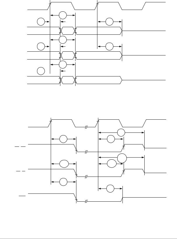
Bus Signal Timing
Figure 9-4 provides the timing for the synchronous output signals.
CLKOUT |
|
|
B8 |
B7 |
B9 |
Output |
|
Signals |
|
|
B8a |
B7a |
B9 |
Output |
|
Signals |
|
B8b
B7b 
Output
Signals
Figure 9-4. Synchronous Output Signals Timing
Figure 9-5 provides the timing for the synchronous active pull-up and open-drain output signals.
CLKOUT
B13
B11 |
B12 |
TS, BB
B13a
B11a |
B12a |
TA, BI
B14
B15
TEA
Figure 9-5. Synchronous Active Pull-Up Resistor and Open-Drain Outputs Signals
Timing
22 |
MPC860 Family Hardware Specifications |
MOTOROLA |

Bus Signal Timing
Figure 9-6 provides the timing for the synchronous input signals.
CLKOUT
B16
B17
TA, BI
B16a
B17a
TEA, KR,
RETRY, CR
B16b
B17
BB, BG, BR
Figure 9-6. Synchronous Input Signals Timing
Figure 9-7 provides normal case timing for input data. It also applies to normal read accesses under the control of the UPM in the memory controller.
CLKOUT
B16
B17
TA
B18
B19
D[0:31],
DP[0:3]
Figure 9-7. Input Data Timing in Normal Case
Figure 9-8 provides the timing for the input data controlled by the UPM for data beats where DLT3 = 1 in the UPM RAM words. (This is only the case where data is latched on the falling edge of CLKOUT.)
MOTOROLA |
MPC860 Family Hardware Specifications |
23 |
 Loading...