


XPC850

查询XPC850供应商
Networking Communication Microprocessors
XPC850 (Rev 0.3)
XPC860
Reliability Report
for
XPC860T
0.42m Single Poly Wafer Fabrication Process
Revision: 5/99

1.0 Purpose and Description
This report summarizes the reliability data for Motorola communication
microprocessors fabricated on the 0.42m single polysilicon process in our wafer
fabrication facility, Mos 11, in Austin, Texas. The current devices fabricated using this
process are given in the table below.
Device Mask Set Design
Revision
XPC850 F98S 0.3 309 x 335 0.42m
XPC860 J24A
H96G
XPC860T J21M 0.2 338 x 347 0.42m
Table 1. Device properties.
All of these devices are currently in their XC phase of product life, which is the
time when design errata are discovered and corrected. Although the 850 and 860 are still
classified as XC devices, they are built using production equipment and processes, and
have completed their reliability qualifications. There are some functional errata on these
devices, which may impact some customers. These errata are expected to be corrected in
revision D of the 860, which we expect to grant MC status to. For a list of current design
errata on these devices, please contact your local Motorola sales person. To locate the
nearest sales office, you can find them on our website at http://mot-sps.com/sales/
sales_web.html
2.0 Assembly / Package Information
B.1
C
Die Size
(mils)
338 x 329
338 x 329
Process
Geometry
0.42m
The XPC850 is assembled in a 256 leaded plastic ball grid array. The XPC860 is
assembled in a 357 lead plastic ball grid array (PBGA). Both packages have been shown
to meet level 3 moisture sensitivity as classified by JEDEC A113. Our volume
production is manufactured in MotorolaÕs Kuala Lumpur, Malaysia facility, however we
have also qualified Citizen Watch Co, in Japan as an alternate assembly site.
2

3.0 Family Qualification Strategy
Motorola uses a ÒfamilyÓ qualification strategy which allows sharing of certain
reliability data across a common design rule / fabrication geometries and packaging types.
Reliability data from other Motorola devices which are designed using the same design
rules and wafer fabrication processes are included with this report.
All of the devices in this report have been in production manufacturing for at least 3
years. The data presented in this report is both data from current production material
and historical data used to qualify devices, processes, and wafer fab and assembly sites.
This report will be updated periodically (typically twice/year) with new reliability data
from subsequent qualifications and reliability monitors.
3
4.0 Qualification Data
Motorola .42m Process Qualification Summary
The following data shows results of our .42m qualifications:
Life Test (+125°C, 4.5V)
Device/Mask Set SS 168 Hrs. 504 Hrs. 1008 Hrs. 2016 Hrs. Failure Details
XPC850 (F98S) rev 0.3 77 1/77 0/76 0/71 --- 168 Hr : Speed degradation failure
1008 Hr: 4 parts missing balls, 1 part
damaged -discounted
XPC850 (F98S) rev 0.3 77 0/77 0/75 0/74 --- 504 /1008 Hr: Damaged part -
discounted
XPC850 (F98S) rev 0.3 77 0/77 0/77 0/72 --- 1008 Hr: Units discounted
XPC850 (F98S) rev 0.3 77 0/77 0/75 0/69 --- 168/504 Hr: Units discounted
XPC860 (J23A) rev A.3 77 0/77 0/77 0/77 0/77 --XPC860 (J23A) rev A.3 77 0/77 0/77 0/77 0/77 ---
XPC860 (J23A) rev A.3 77 0/77 0/77 0/77 0/77 --XPC860 (H96G) rev C.1 77 0/77 0/77 0/77 --XPC860 (H96G) rev C.1 77 0/77 1/77 0/77 --- Functional Failure Ð destroyed in FA
XPC860 (H96G) rev C.1 77 0/77 0/77 0/77 ---
XPC860T (J21M) 77 1/77 0/76 0/75 --- 168 hr: Funct fail, 1008 hr: 1 unit
damaged at test-discounted
68LC060 (G59Y) 77 0/76 0/76 0/63 --- 168/1008 Hr: Parts discounted
68LC060 (G59Y) 77 0/77 0/77 0/77 --- --68LC060 (G59Y) 77 0/77 0/77 0/77 --- --68LC060 (G59Y) 77 0/77 0/77 --- --- --68LC060 (G59Y) 77 1/77 0/76 --- --- 168 Hr: 1 functional fail
Total 1232 3/1231 1/1224 0/1040 0/231 ---
Table 1. Life Test Data.
4
MM
MM
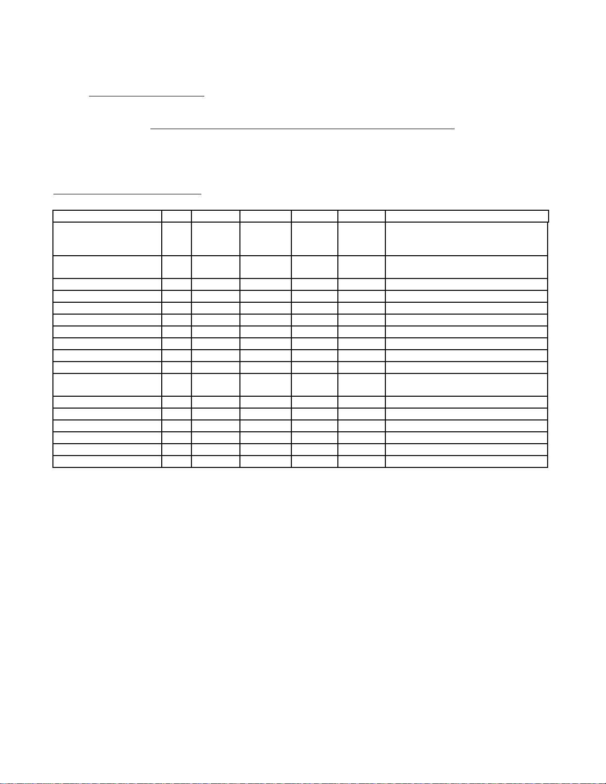
1000.00
100.00
10.00
1.00
Fit Rate (Failures/1E9 Device Hours)
0.10
0 2 0 40 60 80 100 120
FITs vs Junction Temperature: .42u FIT/MTBF Data
Thermal and Voltage Acceleration
eA = 0.5 eV, Beta = 2.5, 90% Confidence
Tj 3 V 3.3 V 3.5 V
40 °C247
60 °C 6 13 22
80 °C 173659
Junction Temperature (°C)
3 V
3.3 V
3.5 V
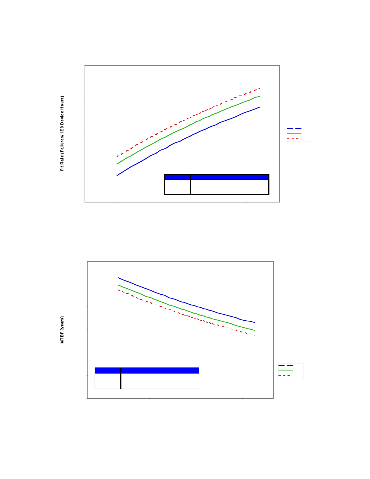
1.00E+06
1.00E+05
1.00E+04
1.00E+03
MTBF (years)
1.00E+02
1.00E+01
1.00E+00
0 20 40 60 80 100 120
MTBF vs Junction Temperature: .42u FIT/MTBF Data
mm
mm
Tj 3 V 3.3 V 3.5 V
40 °C 5.4E+4 2.6E+4 1.6E+4
60 °C 1.8E+4 8.4E+3 5.1E+3
80 °C 6.6E+3 3.1E+3 1.9E+3
eA = 0.5 eV, Beta = 2.5, 90% Confidence
Junction Temperature (°C)
Thermal and Voltage Acceleration
3 V
3.3 V
3.5 V
5
 Loading...