


XC68EZ328ZC16V


Motorola, Incorporated
Semiconductor Products Sector
6501 William Cannon Drive West
Austin TX 78735-8598
MC68EZ328
Integrated Processor
UserÕs Manual
Order this document by
MC68EZ328UM/D
(Motorola Order Number)
Rev. 1, 11/98

©MOTOROLA INC., 1998. All rights reserved.
This document contains information on a new product. Specifications and information herein are subject to change
without notice.
Motorola reserves the right to make changes without further notice to any products herein to improve
reliability, function, or design. Motorola does not assume any liability arising out of the application or use
of any product or circuit described herein; neither does it convey any license under its patent rights nor the
rights of others. Motorola products are not designed, intended, or authorized for use as components in
systems intended for surgical implant into the body, or other application in which the failure of the
Motorola product could create a situation where personal injury or death may occur. Should Buyer
purchase or use Motorola products for any such unintended or unauthorized application, Buyer shall
indemnify and hold Motorola and its officers, employees, subsidiaries, affiliates, and distributors harmless
against all claims, costs, damages, and expenses, and reasonable attorney fees arising out of, directly or
indirectly, any claim of personal injury or death associated with such unintended or unauthorized use,
even if such claim alleges that Motorola was negligent regarding the design or manufacture of the part.
Motorola and
are registered trademarks of Motorola, Inc. Motorola, Inc. is an Equal
Opportunity/Affirmative Action Employer
OnCE and Mfax are trademarks of Motorola, Inc.

MOTOROLA
MC68EZ328 USERÕS MANUAL
v
TABLE OF CONTENTS
Paragraph Page
Number Title Number
PREFACE
Related Documentation. . . . . . . . . . . . . . . . . . . . . . . . . . . . . . . . . . . . . . . . . . . . . . xvii
Organization of This Manual . . . . . . . . . . . . . . . . . . . . . . . . . . . . . . . . . . . . . . . . . . xvii
SECTION 1
BASIC ARCHITECTURE
1.1 Core . . . . . . . . . . . . . . . . . . . . . . . . . . . . . . . . . . . . . . . . . . . . . . . . . . . . . . . 1-2
1.1.1 Core Programming Model . . . . . . . . . . . . . . . . . . . . . . . . . . . . . . . . . . . . 1-2
1.1.2 Data and Address Mode Types. . . . . . . . . . . . . . . . . . . . . . . . . . . . . . . . 1-4
1.1.3 EC000 Instruction Set . . . . . . . . . . . . . . . . . . . . . . . . . . . . . . . . . . . . . . . 1-5
1.2 Chip-Select Logic and Bus Interface . . . . . . . . . . . . . . . . . . . . . . . . . . . . . . 1-6
1.3 Phase-Locked Loop and Power Control. . . . . . . . . . . . . . . . . . . . . . . . . . . . 1-6
1.4 Interrupt Controller . . . . . . . . . . . . . . . . . . . . . . . . . . . . . . . . . . . . . . . . . . . . 1-7
1.5 Parallel General-Purpose I/O Ports . . . . . . . . . . . . . . . . . . . . . . . . . . . . . . . 1-7
1.6 Pulse-Width Modulator . . . . . . . . . . . . . . . . . . . . . . . . . . . . . . . . . . . . . . . . . 1-7
1.7 General-Purpose Timer . . . . . . . . . . . . . . . . . . . . . . . . . . . . . . . . . . . . . . . . 1-7
1.8 Serial Peripheral Interface . . . . . . . . . . . . . . . . . . . . . . . . . . . . . . . . . . . . . . 1-7
1.9 UART and Infra-Red Communication Support . . . . . . . . . . . . . . . . . . . . . . . 1-8
1.10 LCD Controller . . . . . . . . . . . . . . . . . . . . . . . . . . . . . . . . . . . . . . . . . . . . . . . 1-8
1.11 Real-Time Clock . . . . . . . . . . . . . . . . . . . . . . . . . . . . . . . . . . . . . . . . . . . . . . 1-8
1.12 DRAM Controller . . . . . . . . . . . . . . . . . . . . . . . . . . . . . . . . . . . . . . . . . . . . . 1-8
1.13 In-Circuit Emulation Module . . . . . . . . . . . . . . . . . . . . . . . . . . . . . . . . . . . . . 1-8
1.14 Bootstrap Mode . . . . . . . . . . . . . . . . . . . . . . . . . . . . . . . . . . . . . . . . . . . . . . 1-8
1.15 Memory Map. . . . . . . . . . . . . . . . . . . . . . . . . . . . . . . . . . . . . . . . . . . . . . . . . 1-8
SECTION 2
SIGNAL DESCRIPTIONS
2.1 Signals GROUped by Function . . . . . . . . . . . . . . . . . . . . . . . . . . . . . . . . . . 2-3
2.2 POWER and Ground Signals . . . . . . . . . . . . . . . . . . . . . . . . . . . . . . . . . . . . 2-4
2.3 CLOCK and System Control Signals . . . . . . . . . . . . . . . . . . . . . . . . . . . . . . 2-4
2.4 ADDRESS BUS Signals . . . . . . . . . . . . . . . . . . . . . . . . . . . . . . . . . . . . . . . . 2-5
2.5 DATA BUS Signals. . . . . . . . . . . . . . . . . . . . . . . . . . . . . . . . . . . . . . . . . . . . 2-5
2.6 BUS CONTROL Signals. . . . . . . . . . . . . . . . . . . . . . . . . . . . . . . . . . . . . . . . 2-6
2.7 INTERRUPT CONTROLler Signals . . . . . . . . . . . . . . . . . . . . . . . . . . . . . . . 2-6
2.8 LCD CONTROLLER Signals . . . . . . . . . . . . . . . . . . . . . . . . . . . . . . . . . . . . 2-7

vi
MC68EZ328 USERÕS MANUAL
MOTOROLA
2.9 UART Controller Signals . . . . . . . . . . . . . . . . . . . . . . . . . . . . . . . . . . . . . . . 2-8
2.10 TIMER Signal . . . . . . . . . . . . . . . . . . . . . . . . . . . . . . . . . . . . . . . . . . . . . . . . 2-8
2.11 Pulse-Width Modulator Signal . . . . . . . . . . . . . . . . . . . . . . . . . . . . . . . . . . . 2-8
2.12 Serial Peripheral Interface Signals . . . . . . . . . . . . . . . . . . . . . . . . . . . . . . . . 2-8
2.13 CHIP-SELECT Signals. . . . . . . . . . . . . . . . . . . . . . . . . . . . . . . . . . . . . . . . . 2-9
2.14 In-Circuit EMULATion Signals . . . . . . . . . . . . . . . . . . . . . . . . . . . . . . . . . . . 2-9
SECTION 3
SYSTEM CONTROL
3.1 Operation . . . . . . . . . . . . . . . . . . . . . . . . . . . . . . . . . . . . . . . . . . . . . . . . . . . 3-1
3.2 Programming Model . . . . . . . . . . . . . . . . . . . . . . . . . . . . . . . . . . . . . . . . . . . 3-2
3.2.1 System Control Register . . . . . . . . . . . . . . . . . . . . . . . . . . . . . . . . . . . . . 3-2
SECTION 4
CHIP-SELECT LOGIC
4.1 Chip-Select Operation . . . . . . . . . . . . . . . . . . . . . . . . . . . . . . . . . . . . . . . . . 4-2
4.1.1 Memory Protection . . . . . . . . . . . . . . . . . . . . . . . . . . . . . . . . . . . . . . . . . 4-2
4.1.2 Programmable Data Bus Size. . . . . . . . . . . . . . . . . . . . . . . . . . . . . . . . . 4-3
4.1.3 Overlapping Chip-Select Registers. . . . . . . . . . . . . . . . . . . . . . . . . . . . . 4-4
4.2 PROGRAMMING MODEL . . . . . . . . . . . . . . . . . . . . . . . . . . . . . . . . . . . . . . 4-4
4.2.1 Chip-Select Group Base Address Registers. . . . . . . . . . . . . . . . . . . . . . 4-4
4.2.2 Chip-Select Registers . . . . . . . . . . . . . . . . . . . . . . . . . . . . . . . . . . . . . . . 4-5
4.2.3 Emulation Chip-Select Register . . . . . . . . . . . . . . . . . . . . . . . . . . . . . . . 4-8
4.3 Programming Example. . . . . . . . . . . . . . . . . . . . . . . . . . . . . . . . . . . . . . . . . 4-9
SECTION 5
PHASE-LOCKED LOOP AND POWER CONTROL
5.1 Operation . . . . . . . . . . . . . . . . . . . . . . . . . . . . . . . . . . . . . . . . . . . . . . . . . . . 5-2
5.1.1 Using the PLL To Reduce Power Consumption . . . . . . . . . . . . . . . . . . . 5-2
5.1.2 PLL Operation at Power-Up . . . . . . . . . . . . . . . . . . . . . . . . . . . . . . . . . . 5-2
5.1.3 PLL Operation at Wake-Up. . . . . . . . . . . . . . . . . . . . . . . . . . . . . . . . . . . 5-2
5.1.4 Changing the VCO Frequency . . . . . . . . . . . . . . . . . . . . . . . . . . . . . . . . 5-3
5.1.5 PLL Operation at System Shut-Down . . . . . . . . . . . . . . . . . . . . . . . . . . 5-3
5.2 Programming Model . . . . . . . . . . . . . . . . . . . . . . . . . . . . . . . . . . . . . . . . . . . 5-4
5.2.1 PLL Control Register. . . . . . . . . . . . . . . . . . . . . . . . . . . . . . . . . . . . . . . . 5-4
5.2.2 PLL Frequency Select Register . . . . . . . . . . . . . . . . . . . . . . . . . . . . . . . 5-5
5.3 POWER CONTROL . . . . . . . . . . . . . . . . . . . . . . . . . . . . . . . . . . . . . . . . . . . 5-6
5.3.1 Operating the Power Control Module . . . . . . . . . . . . . . . . . . . . . . . . . . . 5-8
5.3.2 Power Control Register. . . . . . . . . . . . . . . . . . . . . . . . . . . . . . . . . . . . . . 5-9
SECTION 6
INTERRUPT CONTROLLER

MOTOROLA
MC68EZ328 USERÕS MANUAL
vii
6.1 Interrupt Processing . . . . . . . . . . . . . . . . . . . . . . . . . . . . . . . . . . . . . . . . . . . 6-1
6.2 Exception Vectors. . . . . . . . . . . . . . . . . . . . . . . . . . . . . . . . . . . . . . . . . . . . . 6-3
6.3 Reset . . . . . . . . . . . . . . . . . . . . . . . . . . . . . . . . . . . . . . . . . . . . . . . . . . . . . . 6-4
6.3.1 DATA BUS WIDTH FOR BOOT DEVICE OPERATION . . . . . . . . . . . . . 6-5
6.4 INTERRUPT CONTROLLER operation . . . . . . . . . . . . . . . . . . . . . . . . . . . . 6-5
6.5 Vector Generator . . . . . . . . . . . . . . . . . . . . . . . . . . . . . . . . . . . . . . . . . . . . . 6-6
6.6 Programming Model . . . . . . . . . . . . . . . . . . . . . . . . . . . . . . . . . . . . . . . . . . . 6-6
6.6.1 Interrupt Vector Register . . . . . . . . . . . . . . . . . . . . . . . . . . . . . . . . . . . . . 6-6
6.6.2 Interrupt Control Register . . . . . . . . . . . . . . . . . . . . . . . . . . . . . . . . . . . . 6-7
6.6.3 Interrupt Mask Register. . . . . . . . . . . . . . . . . . . . . . . . . . . . . . . . . . . . . . 6-9
6.6.4 Interrupt Status Register . . . . . . . . . . . . . . . . . . . . . . . . . . . . . . . . . . . . 6-11
6.6.5 Interrupt Pending Register . . . . . . . . . . . . . . . . . . . . . . . . . . . . . . . . . . 6-16
6.7 KEYBOARD INTERRUPTs . . . . . . . . . . . . . . . . . . . . . . . . . . . . . . . . . . . . 6-20
6.8 PEN Interrupts . . . . . . . . . . . . . . . . . . . . . . . . . . . . . . . . . . . . . . . . . . . . . . 6-20
SECTION 7
PARALLEL PORTS
7.1 Operation . . . . . . . . . . . . . . . . . . . . . . . . . . . . . . . . . . . . . . . . . . . . . . . . . . . 7-1
7.2 Programming Model . . . . . . . . . . . . . . . . . . . . . . . . . . . . . . . . . . . . . . . . . . . 7-2
7.2.1 Port A Registers . . . . . . . . . . . . . . . . . . . . . . . . . . . . . . . . . . . . . . . . . . . 7-2
7.2.2 Port B Registers . . . . . . . . . . . . . . . . . . . . . . . . . . . . . . . . . . . . . . . . . . . 7-3
7.2.3 Port C Registers . . . . . . . . . . . . . . . . . . . . . . . . . . . . . . . . . . . . . . . . . . . 7-5
7.2.4 Port D Registers . . . . . . . . . . . . . . . . . . . . . . . . . . . . . . . . . . . . . . . . . . . 7-7
7.2.5 Port E Registers . . . . . . . . . . . . . . . . . . . . . . . . . . . . . . . . . . . . . . . . . . 7-10
7.2.6 Port F Registers . . . . . . . . . . . . . . . . . . . . . . . . . . . . . . . . . . . . . . . . . . 7-12
7.2.7 Port G Registers . . . . . . . . . . . . . . . . . . . . . . . . . . . . . . . . . . . . . . . . . . 7-14
SECTION 8
PULSE-WIDTH MODULATOR
8.1 Operation . . . . . . . . . . . . . . . . . . . . . . . . . . . . . . . . . . . . . . . . . . . . . . . . . . . 8-1
8.1.1 Playback Mode . . . . . . . . . . . . . . . . . . . . . . . . . . . . . . . . . . . . . . . . . . . . 8-1
8.1.2 Tone Mode . . . . . . . . . . . . . . . . . . . . . . . . . . . . . . . . . . . . . . . . . . . . . . . 8-2
8.1.3 D/A Mode . . . . . . . . . . . . . . . . . . . . . . . . . . . . . . . . . . . . . . . . . . . . . . . . 8-2
8.2 Programming Model . . . . . . . . . . . . . . . . . . . . . . . . . . . . . . . . . . . . . . . . . . . 8-2
8.2.1 PWM Control Register . . . . . . . . . . . . . . . . . . . . . . . . . . . . . . . . . . . . . . 8-2
8.2.2 PWM Sample Register . . . . . . . . . . . . . . . . . . . . . . . . . . . . . . . . . . . . . . 8-5
8.2.3 PWM Period Register . . . . . . . . . . . . . . . . . . . . . . . . . . . . . . . . . . . . . . . 8-5
8.2.4 PWM Counter Register . . . . . . . . . . . . . . . . . . . . . . . . . . . . . . . . . . . . . . 8-6
8.3 Programming Example . . . . . . . . . . . . . . . . . . . . . . . . . . . . . . . . . . . . . . . . . 8-6
SECTION 9
GENERAL-PURPOSE TIMER
9.1 OPERATION . . . . . . . . . . . . . . . . . . . . . . . . . . . . . . . . . . . . . . . . . . . . . . . . 9-1

viii
MC68EZ328 USERÕS MANUAL
MOTOROLA
9.2 Programming Model . . . . . . . . . . . . . . . . . . . . . . . . . . . . . . . . . . . . . . . . . . . 9-2
9.2.1 Timer Control Register . . . . . . . . . . . . . . . . . . . . . . . . . . . . . . . . . . . . . . 9-2
9.2.2 Timer Prescaler Register . . . . . . . . . . . . . . . . . . . . . . . . . . . . . . . . . . . . 9-4
9.2.3 Timer Compare Register. . . . . . . . . . . . . . . . . . . . . . . . . . . . . . . . . . . . . 9-4
9.2.4 Timer Capture Register. . . . . . . . . . . . . . . . . . . . . . . . . . . . . . . . . . . . . . 9-4
9.2.5 Timer Counter Register. . . . . . . . . . . . . . . . . . . . . . . . . . . . . . . . . . . . . . 9-5
9.2.6 Timer Status Register . . . . . . . . . . . . . . . . . . . . . . . . . . . . . . . . . . . . . . . 9-5
SECTION 10
SERIAL PERIPHERAL INTERFACE MASTER
10.1 OPERATION . . . . . . . . . . . . . . . . . . . . . . . . . . . . . . . . . . . . . . . . . . . . . . . 10-1
10.1.1 Phase/Polarity Configurations. . . . . . . . . . . . . . . . . . . . . . . . . . . . . . . . 10-2
10.1.2 Signals . . . . . . . . . . . . . . . . . . . . . . . . . . . . . . . . . . . . . . . . . . . . . . . . . 10-3
10.2 Programming Model . . . . . . . . . . . . . . . . . . . . . . . . . . . . . . . . . . . . . . . . . . 10-3
10.2.1 SPIM Data Register . . . . . . . . . . . . . . . . . . . . . . . . . . . . . . . . . . . . . . . 10-3
10.2.2 SPIM Control/Status Register . . . . . . . . . . . . . . . . . . . . . . . . . . . . . . . . 10-4
10.3 Programming Example. . . . . . . . . . . . . . . . . . . . . . . . . . . . . . . . . . . . . . . . 10-5
SECTION 11
UNIVERSAL ASYNCHRONOUS RECEIVER/TRANSMITTER
11.1 SERIAL OPERATION . . . . . . . . . . . . . . . . . . . . . . . . . . . . . . . . . . . . . . . . 11-2
11.1.1 NRZ Mode. . . . . . . . . . . . . . . . . . . . . . . . . . . . . . . . . . . . . . . . . . . . . . . 11-2
11.1.2 IrDA Mode. . . . . . . . . . . . . . . . . . . . . . . . . . . . . . . . . . . . . . . . . . . . . . . 11-2
11.1.3 SERIAL INTERFACE SIGNALS . . . . . . . . . . . . . . . . . . . . . . . . . . . . . . 11-3
11.2 SUB-BLOCK Operation . . . . . . . . . . . . . . . . . . . . . . . . . . . . . . . . . . . . . . . 11-4
11.2.1 Transmitter . . . . . . . . . . . . . . . . . . . . . . . . . . . . . . . . . . . . . . . . . . . . . . 11-4
11.2.2 Receiver . . . . . . . . . . . . . . . . . . . . . . . . . . . . . . . . . . . . . . . . . . . . . . . . 11-5
11.2.3 Baud Rate Generator . . . . . . . . . . . . . . . . . . . . . . . . . . . . . . . . . . . . . . 11-6
11.3 Programming Model . . . . . . . . . . . . . . . . . . . . . . . . . . . . . . . . . . . . . . . . . . 11-8
11.3.1 UART Status/Control Register . . . . . . . . . . . . . . . . . . . . . . . . . . . . . . . 11-8
11.3.2 UART Baud Control Register . . . . . . . . . . . . . . . . . . . . . . . . . . . . . . . 11-11
11.3.3 UART Receiver Register. . . . . . . . . . . . . . . . . . . . . . . . . . . . . . . . . . . 11-12
11.3.4 UART Transmitter Register. . . . . . . . . . . . . . . . . . . . . . . . . . . . . . . . . 11-14
11.3.5 UART Miscellaneous Register . . . . . . . . . . . . . . . . . . . . . . . . . . . . . . 11-16
11.3.6 UART Non-Integer Prescaler Register . . . . . . . . . . . . . . . . . . . . . . . . 11-18
11.4 Non-Integer Prescaler Programming Example. . . . . . . . . . . . . . . . . . . . . 11-19
SECTION 12
LCD CONTROLLER
12.1 Operation . . . . . . . . . . . . . . . . . . . . . . . . . . . . . . . . . . . . . . . . . . . . . . . . . . 12-2
12.1.1 Connecting the LCD Controller to an LCD Panel . . . . . . . . . . . . . . . . . 12-3
12.1.2 Controlling the Display . . . . . . . . . . . . . . . . . . . . . . . . . . . . . . . . . . . . . 12-4
12.1.3 Using Low-Power Mode . . . . . . . . . . . . . . . . . . . . . . . . . . . . . . . . . . . . 12-8

MOTOROLA
MC68EZ328 USERÕS MANUAL
ix
12.1.4 Using the DMA Controller . . . . . . . . . . . . . . . . . . . . . . . . . . . . . . . . . . . 12-8
12.2 Programming Model . . . . . . . . . . . . . . . . . . . . . . . . . . . . . . . . . . . . . . . . . . 12-9
12.2.1 LCD Screen Starting Address Register. . . . . . . . . . . . . . . . . . . . . . . . . 12-9
12.2.2 LCD Virtual Page Width Register . . . . . . . . . . . . . . . . . . . . . . . . . . . . 12-10
12.2.3 LCD Screen Width Register . . . . . . . . . . . . . . . . . . . . . . . . . . . . . . . . 12-10
12.2.4 LCD Screen Height Register. . . . . . . . . . . . . . . . . . . . . . . . . . . . . . . . 12-11
12.2.5 LCD Cursor X Position Register . . . . . . . . . . . . . . . . . . . . . . . . . . . . . 12-11
12.2.6 LCD Cursor Y Position Register . . . . . . . . . . . . . . . . . . . . . . . . . . . . . 12-12
12.2.7 LCD Cursor Width and Height Register . . . . . . . . . . . . . . . . . . . . . . . 12-12
12.2.8 LCD Blink Control Register . . . . . . . . . . . . . . . . . . . . . . . . . . . . . . . . . 12-13
12.2.9 LCD Panel Interface Configuration Register . . . . . . . . . . . . . . . . . . . . 12-13
12.2.10 LCD Polarity Configuration Register . . . . . . . . . . . . . . . . . . . . . . . . . . 12-14
12.2.11 LACD Rate Control Register . . . . . . . . . . . . . . . . . . . . . . . . . . . . . . . . 12-14
12.2.12 LCD Pixel Clock Divider Register . . . . . . . . . . . . . . . . . . . . . . . . . . . . 12-15
12.2.13 LCD Clocking Control Register . . . . . . . . . . . . . . . . . . . . . . . . . . . . . . 12-15
12.2.14 LCD Refresh Rate Adjustment Register . . . . . . . . . . . . . . . . . . . . . . . 12-16
12.2.15 LCD Panning Offset Register . . . . . . . . . . . . . . . . . . . . . . . . . . . . . . . 12-17
12.2.16 LCD Frame Rate Control Modulation Register . . . . . . . . . . . . . . . . . . 12-17
12.2.17 LCD Gray Palette Mapping Register. . . . . . . . . . . . . . . . . . . . . . . . . . 12-18
12.2.18 PWM Contrast Control Register . . . . . . . . . . . . . . . . . . . . . . . . . . . . . 12-18
12.3 Programming EXAMPLE . . . . . . . . . . . . . . . . . . . . . . . . . . . . . . . . . . . . . 12-19
SECTION 13
REAL-TIME CLOCK
13.1 Operation . . . . . . . . . . . . . . . . . . . . . . . . . . . . . . . . . . . . . . . . . . . . . . . . . . 13-2
13.1.1 Prescaler and Counter . . . . . . . . . . . . . . . . . . . . . . . . . . . . . . . . . . . . . 13-2
13.1.2 Alarm. . . . . . . . . . . . . . . . . . . . . . . . . . . . . . . . . . . . . . . . . . . . . . . . . . . 13-3
13.1.3 Watchdog Timer . . . . . . . . . . . . . . . . . . . . . . . . . . . . . . . . . . . . . . . . . . 13-3
13.1.4 Sampling Timer . . . . . . . . . . . . . . . . . . . . . . . . . . . . . . . . . . . . . . . . . . . 13-3
13.1.5 Minute Stopwatch . . . . . . . . . . . . . . . . . . . . . . . . . . . . . . . . . . . . . . . . . 13-4
13.2 Programming Model . . . . . . . . . . . . . . . . . . . . . . . . . . . . . . . . . . . . . . . . . . 13-4
13.2.1 RTC Hours, Minutes, and Seconds Register . . . . . . . . . . . . . . . . . . . . 13-4
13.2.2 RTC Alarm Register . . . . . . . . . . . . . . . . . . . . . . . . . . . . . . . . . . . . . . . 13-5
13.2.3 Watchdog Timer Register . . . . . . . . . . . . . . . . . . . . . . . . . . . . . . . . . . . 13-5
13.2.4 RTC Control Register . . . . . . . . . . . . . . . . . . . . . . . . . . . . . . . . . . . . . . 13-6
13.2.5 RTC Interrupt Status Register. . . . . . . . . . . . . . . . . . . . . . . . . . . . . . . . 13-7
13.2.6 RTC Interrupt Enable Register . . . . . . . . . . . . . . . . . . . . . . . . . . . . . . . 13-9
13.2.7 Stopwatch Minutes Register . . . . . . . . . . . . . . . . . . . . . . . . . . . . . . . . 13-11
13.2.8 RTC Day Count Register . . . . . . . . . . . . . . . . . . . . . . . . . . . . . . . . . . 13-12
13.2.9 RTC Day Alarm Register. . . . . . . . . . . . . . . . . . . . . . . . . . . . . . . . . . . 13-12
SECTION 14
DRAM CONTROLLER
14.1 OPERATION . . . . . . . . . . . . . . . . . . . . . . . . . . . . . . . . . . . . . . . . . . . . . . . 14-2

x
MC68EZ328 USERÕS MANUAL
MOTOROLA
14.1.1 Address Multiplexing. . . . . . . . . . . . . . . . . . . . . . . . . . . . . . . . . . . . . . . 14-2
14.1.2 DTACK
Generation . . . . . . . . . . . . . . . . . . . . . . . . . . . . . . . . . . . . . . . . 14-3
14.1.3 Refresh Control. . . . . . . . . . . . . . . . . . . . . . . . . . . . . . . . . . . . . . . . . . . 14-3
14.1.4 LCD Interface . . . . . . . . . . . . . . . . . . . . . . . . . . . . . . . . . . . . . . . . . . . . 14-3
14.1.5 8-Bit Mode . . . . . . . . . . . . . . . . . . . . . . . . . . . . . . . . . . . . . . . . . . . . . . 14-4
14.1.6 Low-Power Standby Mode . . . . . . . . . . . . . . . . . . . . . . . . . . . . . . . . . . 14-4
14.1.7 Data Retention During Reset . . . . . . . . . . . . . . . . . . . . . . . . . . . . . . . . 14-5
14.2 Programming Model . . . . . . . . . . . . . . . . . . . . . . . . . . . . . . . . . . . . . . . . . . 14-6
14.2.1 DRAM Memory Configuration Register. . . . . . . . . . . . . . . . . . . . . . . . . 14-6
14.2.2 DRAM Control Register . . . . . . . . . . . . . . . . . . . . . . . . . . . . . . . . . . . . 14-8
SECTION 15
IN-CIRCUIT EMULATION
15.1 OPERATION . . . . . . . . . . . . . . . . . . . . . . . . . . . . . . . . . . . . . . . . . . . . . . . 15-2
15.1.1 Entering Emulation Mode . . . . . . . . . . . . . . . . . . . . . . . . . . . . . . . . . . . 15-2
15.1.2 Detecting Breakpoints. . . . . . . . . . . . . . . . . . . . . . . . . . . . . . . . . . . . . . 15-2
15.1.3 Using the Signal Decoder . . . . . . . . . . . . . . . . . . . . . . . . . . . . . . . . . . . 15-3
15.1.4 Using the Interrupt Gate Module. . . . . . . . . . . . . . . . . . . . . . . . . . . . . . 15-3
15.1.5 Using the A-Line Insertion Unit . . . . . . . . . . . . . . . . . . . . . . . . . . . . . . . 15-3
15.2 Programming Model . . . . . . . . . . . . . . . . . . . . . . . . . . . . . . . . . . . . . . . . . . 15-4
15.2.1 In-Circuit Emulation Module Address Compare/Mask Registers . . . . . 15-4
15.2.2 In-Circuit Emulation Module Control Compare/Mask Register . . . . . . . 15-5
15.2.3 In-Circuit Emulation Module Control Register. . . . . . . . . . . . . . . . . . . . 15-6
15.2.4 In-Circuit Emulation Module Status Register . . . . . . . . . . . . . . . . . . . . 15-8
15.3 Typical Design Programming Example . . . . . . . . . . . . . . . . . . . . . . . . . . . 15-8
15.3.1 Host Interface . . . . . . . . . . . . . . . . . . . . . . . . . . . . . . . . . . . . . . . . . . . . 15-9
15.3.2 Dedicated Debug Monitor Memory . . . . . . . . . . . . . . . . . . . . . . . . . . . 15-10
15.3.3 Emulation Memory Mapping FPGA and Emulation Memory . . . . . . . 15-10
15.3.4 Optional Extra Hardware Breakpoint . . . . . . . . . . . . . . . . . . . . . . . . . 15-10
15.3.5 Optional Trace Module . . . . . . . . . . . . . . . . . . . . . . . . . . . . . . . . . . . . 15-10
15.4 Plug-In Emulator Design Example . . . . . . . . . . . . . . . . . . . . . . . . . . . . . . 15-10
15.5 Application Development Design Example . . . . . . . . . . . . . . . . . . . . . . . 15-12
SECTION 16
BOOTSTRAP MODE
16.1 operation . . . . . . . . . . . . . . . . . . . . . . . . . . . . . . . . . . . . . . . . . . . . . . . . . . 16-1
16.1.1 Entering Bootstrap Mode . . . . . . . . . . . . . . . . . . . . . . . . . . . . . . . . . . . 16-1
16.1.2 Bootstrap Record Format . . . . . . . . . . . . . . . . . . . . . . . . . . . . . . . . . . . 16-2
16.1.3 Setting Up the RS-232 Terminal . . . . . . . . . . . . . . . . . . . . . . . . . . . . . . 16-3
16.1.4 Changing the Speed of Communication . . . . . . . . . . . . . . . . . . . . . . . . 16-3
16.2 System Initialization Programming Example . . . . . . . . . . . . . . . . . . . . . . . 16-3
16.3 Application Programming Example . . . . . . . . . . . . . . . . . . . . . . . . . . . . . . 16-4
16.4 Instruction Buffer Usage Example . . . . . . . . . . . . . . . . . . . . . . . . . . . . . . . 16-5
16.5 Bootloader Flowchart . . . . . . . . . . . . . . . . . . . . . . . . . . . . . . . . . . . . . . . . . 16-6

MOTOROLA
MC68EZ328 USERÕS MANUAL
xi
16.6 Special Notes . . . . . . . . . . . . . . . . . . . . . . . . . . . . . . . . . . . . . . . . . . . . . . . 16-7
SECTION 17
APPLICATION GUIDE
17.1 Design Checklist. . . . . . . . . . . . . . . . . . . . . . . . . . . . . . . . . . . . . . . . . . . . . 17-1
17.2 Using the MC68EZ328ADS Board . . . . . . . . . . . . . . . . . . . . . . . . . . . . . . . 17-2
SECTION 18
ELECTRICAL CHARACTERISTICS
18.1 MAXIMUM RATINGs . . . . . . . . . . . . . . . . . . . . . . . . . . . . . . . . . . . . . . . . . 18-1
18.2 DC ELECTRICAL CharacteristicS . . . . . . . . . . . . . . . . . . . . . . . . . . . . . . . 18-1
18.3 AC ELECTRICAL Characteristics. . . . . . . . . . . . . . . . . . . . . . . . . . . . . . . . 18-2
18.3.1 CLKO reference to Chip-Select Signals Timing . . . . . . . . . . . . . . . . . . 18-2
18.3.2 Chip-Select Read Cycle Timing . . . . . . . . . . . . . . . . . . . . . . . . . . . . . . 18-3
18.3.3 Chip-Select Write Cycle Timing . . . . . . . . . . . . . . . . . . . . . . . . . . . . . . 18-4
18.3.4 Chip-Select Flash Write Cycle Timing. . . . . . . . . . . . . . . . . . . . . . . . . . 18-5
18.3.5 DRAM Read Cycle 16-Bit Access (CPU Bus Master). . . . . . . . . . . . . . 18-6
18.3.6 DRAM Write Cycle 16-Bit Access (CPU Bus Master) . . . . . . . . . . . . . . 18-7
18.3.7 DRAM Hidden Refresh Cycle (Normal Mode). . . . . . . . . . . . . . . . . . . . 18-8
18.3.8 DRAM Hidden Refresh Cycle (Low Power Mode) . . . . . . . . . . . . . . . . 18-9
18.3.9 LCD SRAM/ROM DMA Cycle 16-Bit Mode Access(1 ws) ( . . . . . . . . 18-10
18.3.10 LCD DRAM DMA Cycle 16-Bit EDO Mode Access (LCD Bus Master)18-11
18.3.11 LCD DRAM DMA Cycle 16-Bit Page Mode Access (LCD Bus Master)18-12
18.3.12 LCD Controller Timing. . . . . . . . . . . . . . . . . . . . . . . . . . . . . . . . . . . . . 18-13
18.3.13 Normal Mode Timing. . . . . . . . . . . . . . . . . . . . . . . . . . . . . . . . . . . . . . 18-14
18.3.14 Normal Mode and Emulation Mode Timing. . . . . . . . . . . . . . . . . . . . . 18-14
18.3.15 Emulation Mode Timing . . . . . . . . . . . . . . . . . . . . . . . . . . . . . . . . . . . 18-14
18.3.16 Bootstrap Mode Timing . . . . . . . . . . . . . . . . . . . . . . . . . . . . . . . . . . . . 18-15
SECTION 19
MECHANICAL DATA AND ORDERING INFORMATION
19.1 Ordering Information. . . . . . . . . . . . . . . . . . . . . . . . . . . . . . . . . . . . . . . . . . 19-1
19.2 TQFP Pin Assignments . . . . . . . . . . . . . . . . . . . . . . . . . . . . . . . . . . . . . . . 19-2
19.3 TQFP Package Dimensions . . . . . . . . . . . . . . . . . . . . . . . . . . . . . . . . . . . . 19-2
19.4 PBGA Pin Assignments . . . . . . . . . . . . . . . . . . . . . . . . . . . . . . . . . . . . . . . 19-4
19.5 PBGA Package Dimensions. . . . . . . . . . . . . . . . . . . . . . . . . . . . . . . . . . . . 19-4

xii
MC68EZ328 USERÕS MANUAL
MOTOROLA

MOTOROLA
MC68EZ328 USERÕS MANUAL
xiii
LIST OF ILLUSTRATIONS
Figure Page
Number Title Number
1-1 MC68EZ328 Block Diagram . . . . . . . . . . . . . . . . . . . . . . . . . . . . . . . . . . 1-2
1-2 User Programming Model . . . . . . . . . . . . . . . . . . . . . . . . . . . . . . . . . . . . 1-3
1-3 Supervisor Programming Model Supplement . . . . . . . . . . . . . . . . . . . . . 1-3
1-4 MC68EZ328 System Memory Map . . . . . . . . . . . . . . . . . . . . . . . . . . . . . 1-9
2-1 Signals Grouped by Function . . . . . . . . . . . . . . . . . . . . . . . . . . . . . . . . . 2-2
2-2 Typical Crystal Connection . . . . . . . . . . . . . . . . . . . . . . . . . . . . . . . . . . . 2-4
4-1 Chip-Selects and Memory Types . . . . . . . . . . . . . . . . . . . . . . . . . . . . . . 4-1
4-2 Size Selection and Memory Protection for CSB0 and CSB1 . . . . . . . . . 4-3
5-1 PLL Block Diagram . . . . . . . . . . . . . . . . . . . . . . . . . . . . . . . . . . . . . . . . . 5-1
5-2 Power Control Module Block Diagram . . . . . . . . . . . . . . . . . . . . . . . . . . 5-7
5-3 Power Control Operation. . . . . . . . . . . . . . . . . . . . . . . . . . . . . . . . . . . . . 5-8
6-1 Interrupt Processing Flowchart . . . . . . . . . . . . . . . . . . . . . . . . . . . . . . . . 6-2
7-1 Parallel Port Operation . . . . . . . . . . . . . . . . . . . . . . . . . . . . . . . . . . . . . . 7-1
7-2 Interrupt Port Operation . . . . . . . . . . . . . . . . . . . . . . . . . . . . . . . . . . . . . 7-7
8-1 Pulse-Width Modulator Block Diagram . . . . . . . . . . . . . . . . . . . . . . . . . . 8-1
8-2 Audio Waveform Generation. . . . . . . . . . . . . . . . . . . . . . . . . . . . . . . . . . 8-2
9-1 General-Purpose Timer Block Diagram . . . . . . . . . . . . . . . . . . . . . . . . . 9-1
10-1 Serial Peripheral Interface Master Block Diagram . . . . . . . . . . . . . . . . 10-1
10-2 Serial Peripheral Interface Master Operation . . . . . . . . . . . . . . . . . . . . 10-2
11-1 UART Block Diagram . . . . . . . . . . . . . . . . . . . . . . . . . . . . . . . . . . . . . . 11-2
11-2 NRZ ASCII ÒAÓ Character with Odd Parity . . . . . . . . . . . . . . . . . . . . . . 11-2
11-3 IrDA ASCII ÒAÓ Character with Odd Parity. . . . . . . . . . . . . . . . . . . . . . . 11-3
11-4 Baud Rate Generator Block Diagram . . . . . . . . . . . . . . . . . . . . . . . . . . 11-6
12-1 LCD Controller Block Diagram . . . . . . . . . . . . . . . . . . . . . . . . . . . . . . . 12-2
12-2 LCD Interface Timing for 4-, 2-, and 1-Bit Data Widths. . . . . . . . . . . . . 12-4
12-3 LCD Screen Format . . . . . . . . . . . . . . . . . . . . . . . . . . . . . . . . . . . . . . . 12-5
12-4 Mapping Memory Data on the Screen . . . . . . . . . . . . . . . . . . . . . . . . . 12-6
13-1 Real-Time Clock Block Diagram . . . . . . . . . . . . . . . . . . . . . . . . . . . . . . 13-2
14-1 DRAM Controller Block Diagram . . . . . . . . . . . . . . . . . . . . . . . . . . . . . 14-1
14-2 DRAM Address Multiplexer Options. . . . . . . . . . . . . . . . . . . . . . . . . . . 14-2

xiv
MC68EZ328 USERÕS MANUAL
MOTOROLA
14-3 LCD Controller and DRAM Controller Interface . . . . . . . . . . . . . . . . . . 14-4
14-4 Data Retention for the Reset Cycle . . . . . . . . . . . . . . . . . . . . . . . . . . . 14-5
15-1 In-Circuit Emulation Module Block Diagram . . . . . . . . . . . . . . . . . . . . . 15-1
15-2 Typical Emulator Design Example . . . . . . . . . . . . . . . . . . . . . . . . . . . . 15-9
15-3 Plug-in Emulator Design Example . . . . . . . . . . . . . . . . . . . . . . . . . . . 15-11
15-4 Application Development System Design Example . . . . . . . . . . . . . . 15-12
16-1 Bootstrap Mode Reset Timing . . . . . . . . . . . . . . . . . . . . . . . . . . . . . . . 16-2
16-2 Bootloader Program Operation . . . . . . . . . . . . . . . . . . . . . . . . . . . . . . . 16-6
19-1 Top View . . . . . . . . . . . . . . . . . . . . . . . . . . . . . . . . . . . . . . . . . . . . . . . . 19-2

MOTOROLA
MC68EZ328 USERÕS MANUAL
xv
LIST OF TABLES
Table Page
Number Title Number
1-1 Address Modes . . . . . . . . . . . . . . . . . . . . . . . . . . . . . . . . . . . . . . . . . . . . 1-4
1-2 Instruction Set . . . . . . . . . . . . . . . . . . . . . . . . . . . . . . . . . . . . . . . . . . . . 1-5
1-3 ProgrammerÕs Memory Map . . . . . . . . . . . . . . . . . . . . . . . . . . . . . . . . . 1-10
2-1 Signal Function Groups. . . . . . . . . . . . . . . . . . . . . . . . . . . . . . . . . . . . . . 2-3
6-1 Exception Vector Assignment . . . . . . . . . . . . . . . . . . . . . . . . . . . . . . . . 6-3
6-2 Interrupt Vector Numbers . . . . . . . . . . . . . . . . . . . . . . . . . . . . . . . . . . . . 6-6
11-1 Non-Integer Prescaler Values . . . . . . . . . . . . . . . . . . . . . . . . . . . . . . . . 11-7
11-2 Non-Integer Prescaler Settings . . . . . . . . . . . . . . . . . . . . . . . . . . . . . . . 11-7
11-3 Selected Baud Rate Settings . . . . . . . . . . . . . . . . . . . . . . . . . . . . . . . . 11-7
12-1 Gray-Scale Palette Options. . . . . . . . . . . . . . . . . . . . . . . . . . . . . . . . . . 12-7
13-1 Sampling Timer Frequencies . . . . . . . . . . . . . . . . . . . . . . . . . . . . . . . . 13-3

xvi
MC68EZ328 USERÕS MANUAL
MOTOROLA

MOTOROLA
MC68EZ328 USERÕS MANUAL
xvii
PREFACE
The MC68EZ328 (DragonBallEZ) microprocessor, which is the second generation of the
DragonBall
ª
, is designed to save you time, power, cost, board space, pin count, and
programming steps when designing your product. This functionality on a different
microprocessor could require 20 separate components, each with 16-64 separate pins.
These components take up valuable space on your board and they also consume more
power. In addition, the signals between the CPU and a peripheral could be incompatible and
may not run from the same clock, which could require time delays or other special design
constraints.
All this combined makes the MC68EZ328 the microprocessor of choice among many
system designers. Its functionality and glue logic are all optimally connected, timed with the
same clock, fully tested, and uniformly documented. Also, only the essential signals are
brought out to the pins. The MC68EZ328Õs primary package consists of a surface-mount
plastic TQFP designed to leave the smallest possible footprint on your board.
RELATED DOCUMENTATION
This manual will discuss the details of how to initialize, configure, and program the
MC68EZ328 microprocessor. However, it assumes you have a basic knowledge of 68K
architecture. If you are not familiar with 68K, you should get a copy of the following
documents to use in conjunction with this manual.
¥
M68000 UserÕs Manual
(part number M68000UM/AD).
¥
M68EZ328ADS UserÕs Manual
, which is only available from our website.
¥
M68000 ProgrammerÕs Reference Manual
(part number M68000PM/AD).
You can go to the Motorola website at www.mot.com/dragonball and download these
documents or you can contact your local sales office and request a printed version. The
website also has application notes that may be useful to you.
ORGANIZATION OF THIS MANUAL
This manual is organized according to the MC68EZ328 memory map, which is discussed in
Section 1.15 Memory Map.

Preface
xviii
MC68EZ328 USERÕS MANUAL
MOTOROLA

MOTOROLA
MC68EZ328 USERÕS MANUAL
1-1
SECTION 1
BASIC ARCHITECTURE
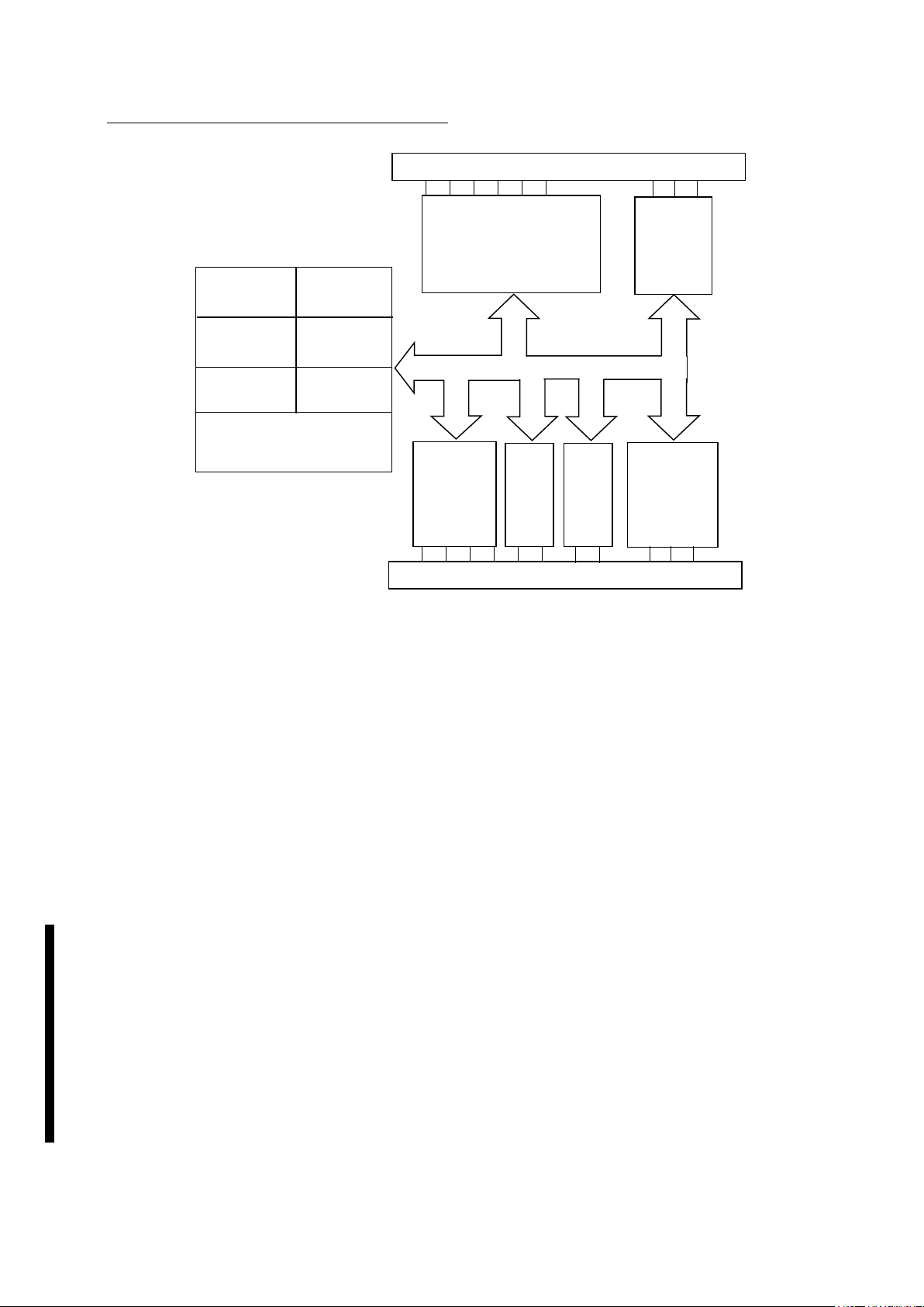
To improve total system throughput and reduce component count, board size, and cost of
system implementation, the MC68EZ328 combines a powerful MC68EC000 processor with
intelligent peripheral modules and a typical system interface logic. The architecture of the
MC68EZ328 consists of the following blocks:
¥ EC000 core
¥ Chip-select logic and bus interface
¥ Phase-locked loop and power control
¥ Interrupt controller
¥ Parallel general-purpose I/O ports
¥ Pulse-width modulator
¥ General-purpose timer
¥ Serial peripheral interface
¥ UART and infra-red communication support
¥ LCD controller
¥ Real-time clock
¥ DRAM controller
¥ In-circuit emulation module
¥ Bootstrap mode
This manual assumes you are familiar with 68K architecture. If you are not, get a copy of the
M68000 UserÕs Manual
(part number M68000UM/AD) and
M68000 ProgrammerÕs
Reference Manual
(part number M68000PM/AD) from your local Motorola sales office.
Basic Architecture
1-2
MC68EZ328 USERÕS MANUAL
MOTOROLA
1.1 CORE
The MC68EC000 core in the MC68EZ328 is an updated implementation of the M68000
32-bit microprocessor architecture. The main features of the core are:
¥ Low power, static HCMOS implementation
¥ 32-bit address bus and 16-bit data bus
¥ Sixteen 32-bit data and address registers
¥ 56 powerful instruction types that support high-level development languages
¥ 14 addressing modes and five main data types
¥ Seven priority levels for interrupt control
The core is completely code-compatible with other members of the M68000 families, which
means it has access to a broad base of established real-time kernels, operating systems,
languages, applications, and development tools.
1.1.1 Core Programming Model
The core has 32-bit registers and a 32-bit program counter, which are shown in Figure 1-2.
The first eight registers (D7ÐD0) are data registers that are used for byte (8-bit), word
(16-bit), and long-word (32-bit) operations. When using the data registers to manipulate
data, they affect the status register (SR). The next seven registers (A6ÐA0) and the user
Figure 1-1. MC68EZ328 Block Diagram
16-BIT
TIMER
MODULE
68EC000 HCMOS
STATIC
CORE
UART
WITH
INFRA-RED
SUPPORT
SPI
LCD
CONTROLLER
SYSTEM INTEGRATION MODULE
INTERRUPT
CONTROLLER
EMULATION
PHASE-LOCKED
LOOP AND
68EC000 INTERNAL BUS
8-/16-BIT
68000 BUS
INTERFACE
ENHANCED
PWM
DRAM
CONTROLLER
REAL-TIME
PARALLEL I/O PORTS
PARALLEL I/O PORTS
BOOTSTRAP
MODE
CLOCK
IN-CIRCUIT
POWER CONTROL

Basic Architecture
MOTOROLA
MC68EZ328 USERÕS MANUAL
1-3
stack pointer (USP) can function as software stack pointers and base address registers.
These registers can be used for word and long-word operations, but they do not affect the
status register. The D7-D0 and A6-A0 registers can be used as index registers.
In supervisor mode, the upper byte of the status register and the supervisor stack pointer
(SSP) can also be programmed, as shown in Figure 1-3.
The status register contains the interrupt mask with seven available levels, as well as an
extend (X), negative (N), zero (Z), overflow (V), and carry (C) condition code. The T bit
indicates when the processor is in trace mode and the S bit indicates when it is in supervisor
or user mode.
Figure 1-2. User Programming Model
Figure 1-3. Supervisor Programming Model Supplement
DATA REGISTERS
ADDRESS REGISTERS
31 16 15
8
7
0
USER STACK POINTER
A7 (USP)
D0
D1
D2
D3
D4
D5
D6
D7
A0
A1
A2
A3
A4
A5
A6
0151631
31 16 15 0
31 0
0
PC
PROGRAM COUNTER
STATUS REGISTER
SR
7
SUPERVISOR STACKA7 (SSP)
31 16 15 0
POINTER
15
0
78
SR STATUS REGISTER
Basic Architecture
1-4
MC68EZ328 USERÕS MANUAL
MOTOROLA
1.1.2 Data and Address Mode Types
The core supports five types of data and six main types of address modes, as described in
the following tables.
DATA TYPES ADDRESS MODE TYPES
Bits Register direct
Binary-coded decimal digits Register indirect
Bytes Absolute
Words Program counter relative
Long words Immediate
Implied
Table 1-1. Address Modes
ADDRESS MODE SYNTAX
Register direct address
Data register direct
Address register direct
Dn
An
Absolute data address
Absolute short
Absolute long
xxx.W
xxx.L
Program counter relative address
Relative with offset
Relative with index offset
d
16
(PC)
d
8
(PC, Xn)
Register indirect address register
Register indirect
Postincrement register indirect
Predecrement register indirect
Register indirect with offset
Indexed register indirect with offset
(An)
(An)+
Ð(An)
d
16
(An)
d
8
(An, Xn)
Immediate data address
Immediate
Quick immediate
#xxx
#1Ð#8
Implied address
Implied register
SR/USP/SP/PC
NOTE:
Dn = Data Register
An = Address Register
Xn = Address or Data Register Used as Index Register
SR = Status Register
PC = Program Counter
SP = Stack Pointer
USP = User Stack Pointer
<> = Effective Address
d
8
= 8-Bit Offset (Displacement)
d
16
= 16-Bit Offset (Displacement)
#xxx = Immediate Data
Basic Architecture
MOTOROLA MC68EZ328 USERÕS MANUAL 1-5
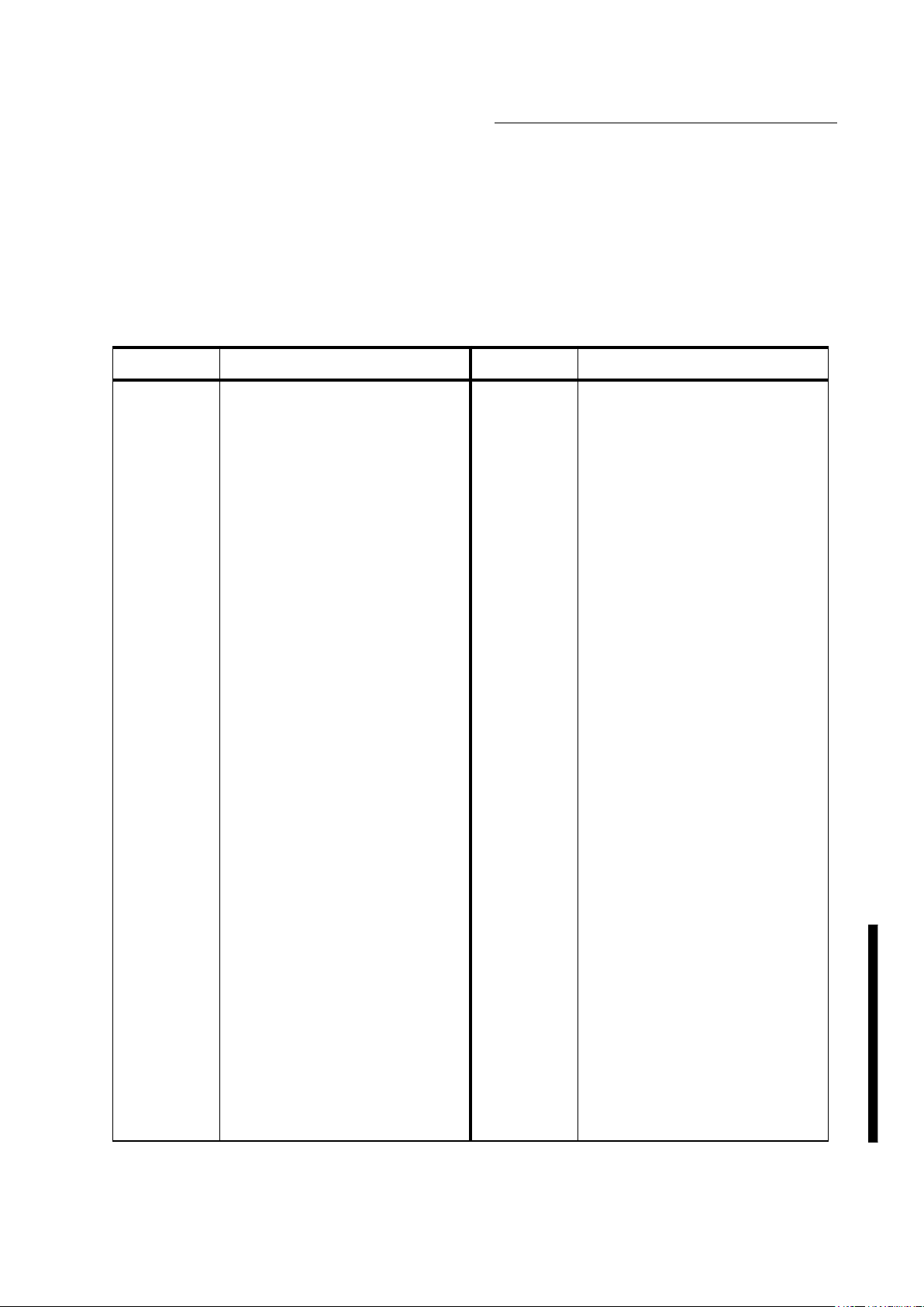
1.1.3 EC000 Instruction Set
The EC000 core instruction set supports high-level languages that facilitate programming.
Almost every instruction operates on bytes, words, and long-words, and most of them can
use any of the 14 address modes. By combining instruction types, data types, and address
modes, you can have access to over 1,000 instructions. These instructions include signed
and unsigned, multiply and divide, quick arithmetic operations, binary-coded decimal (BCD)
arithmetic, and expanded operations (through traps).
Table 1-2. Instruction Set
MNEMONIC DESCRIPTION MNEMONIC DESCRIPTION
ABCD Add decimal with extend MOVEM Move multiple registers
ADD Add MOVEP Move peripheral data
ADDA Add address MOVEQ Move quick
ADDQ Add quick MOVE from SR Move from status register
ADDI Add immediate MOVE to SR Move to status register
ADDX Add with extend MOVE to CCR Move to condition codes
AND Logical AND MOVE USP Move user stack pointer
ANDI AND immediate MULS Signed multiply
ANDI to CCR AND immediate to condition codes MULU Unsigned multiply
ANDI to SR AND immediate to status register NBCD Negate decimal with extend
ASL Arithmetic shift left NEG Negate
ASR Arithmetic shift right NEGX Negate with extend
Bcc Branch conditionally NOP No operation
BCHG Bit test and change NOT Ones complement
BCLR Bit test and clear OR Logical OR
BRA Branch always ORI OR immediate
BSET Bit test and set ORI to CCR OR immediate to condition codes
BSR Branch to subroutine ORI to SR OR immediate to status register
BTST Bit test PEA Push effective address
CHK Check register against bounds RESET Reset external devices
CLR Clear operand ROL Rotate left without extend
CMP Compare ROR Rotate right without extend
CMPA Compare address ROXL Rotate left with extend
CMPM Compare memory ROXR Rotate right with extend
CMPI Compare immediate RTE Return from exception
DBcc Test cond, decrement and branch RTR Return and restore
DIVS Signed divide RTS Return from subroutine
DIVU Unsigned divide SBCD Subtract decimal with extend
Basic Architecture
1-6 MC68EZ328 USERÕS MANUAL MOTOROLA
1.2 CHIP-SELECT LOGIC AND BUS INTERFACE
The system control register (SCR) allows you to configure the system status and control
logic, register double-mapping, bus error generation, and module control register protection
on the MC68EZ328.
The MC68EZ328 contains eight programmable general-purpose chip-select signals. Each
chip-select block allows you to choose whether the chip-select allows read-only or both read
and write accesses, whether a DTACK
signal is automatically generated for the chip-select,
the number of wait states (from zero to six) until the DTACK
will be generated, and an 8- or
16-bit data bus.
The external bus interface handles the transfer of information between the internal core and
the memory, peripherals, or other processing elements in the external address space. It
consists of a 16-bit M68000 data bus interface for internal-only devices and an 8- or 16-bit
(or mixed) data bus interface to external devices.
1.3 PHASE-LOCKED LOOP AND POWER CONTROL
The clock synthesizer can operate with either an external crystal or an external oscillator
using an internal phase-locked loop (PLL). An external clock can also be used to directly
drive the clock signal at the operational frequency.
You can save power on the MC68EZ328 by turning off peripherals that are not being used,
reducing processor clock speed, or disabling the processor altogether. An interrupt at the
EOR Exclusive OR Scc Set conditional
EORI Exclusive OR immediate STOP Stop
EORI to CCR Exclusive OR immediate to condition
codes
SUB Subtract
EORI to SR Exclusive OR immediate to status
register
SUBA Subtract address
EXG Exchange registers SUBI Subtract immediate
EXT Sign extend SUBQ Subtract quick
JMP Jump SUBX Subtract with extend
JSR Jump to subroutine SWAP Swap data register halves
LEA Load effective address TAS Test and set operand
LINK Link stack TRAP Trap
LSL Logical shift left TRAPV Trap on overflow
LSR Logical shift right TST Test
MOVE Move UNLK Unlink
MOVEA Move address
Table 1-2. Instruction Set (Continued)
MNEMONIC DESCRIPTION MNEMONIC DESCRIPTION

Basic Architecture
MOTOROLA MC68EZ328 USERÕS MANUAL 1-7
interrupt controller logic that runs during low-power mode allows you to wake up from this
mode. Programmable interrupt sources cause the system to wake up. On-chip peripherals
can initiate a wake-up from doze mode and the external interrupts and real-time clock can
wake up the core from sleep mode.
1.4 INTERRUPT CONTROLLER
The interrupt controller prioritizes internal and external interrupt requests and generates a
vector number during the CPU interrupt-acknowledge cycle. Interrupt nesting is also
provided so that an interrupt service routine of a lower priority interrupt may be suspended
by a higher priority interrupt request. The on-chip interrupt controller has the following
features:
¥ Prioritized interrupts
¥ Fully nested interrupt environment
¥ Programmable vector generation
¥ Unique vector number generated for each interrupt level
¥ Interrupt/wakeup masking
1.5 PARALLEL GENERAL-PURPOSE I/O PORTS
The MC68EZ328 supports a maximum of 45 general-purpose I/O ports that you can
configure as general-purpose I/O pins or dedicated peripheral interface pins. Each pin can
be independently programmed as a general-purpose I/O pin even when other pins related
to that on-chip peripheral are used as dedicated pins. If all the pins for a particular peripheral
are configured as general-purpose I/O, the peripheral will still operate normally.
1.6 PULSE-WIDTH MODULATOR
The pulse-width modulator (PWM) can be used to generate sound. The 5-byte FIFO can
enhance performance by allowing the CPU to service other interrupts while data is being
supplied to the PWM.
1.7 GENERAL-PURPOSE TIMER
The free-running 16-bit timer can be used in various modes to capture the timer value with
an external event, to trigger an external event or interrupt when the timer reaches a set
value, or to count external events. The timer has an 8-bit prescaler to allow a programmable
clock input frequency to be derived from the system clock.
1.8 SERIAL PERIPHERAL INTERFACE
The serial peripheral interface (SPI) is mainly used for controlling external peripherals. The
passed data is synchronized with the SPI clock and it is transmitted and received with the
same SPI clock. The SPI module is only in master mode, which initiates SPI transfers from
the MC68EZ328 to the peripheral.

Basic Architecture
1-8 MC68EZ328 USERÕS MANUAL MOTOROLA
1.9 UART AND INFRA-RED COMMUNICATION SUPPORT
The UART communicates with external devices with a standard asynchronous protocol at
baud rates from 300 bps to 1152 kpbs. The UART provides the pulses to directly drive
standard IrDA transceivers.
1.10 LCD CONTROLLER
The LCD controller is used to display data on an LCD module. It fetches display data from
memory and provides control signals, frame line pulse, clocks, and data to the LCD module.
It supports monochrome STN LCD modules with a maximum of sixteen gray levels with
frame rate control. System RAM can be used as display memory and DMA frees the CPU
from panel refresh responsibilities.
1.11 REAL-TIME CLOCK
A real-time clock provides time-of-day with one-second resolution. It uses the crystal (either
32.768 KHz or 38.4kHz) as a clock source to keep proper time. It keeps time as long as
power is applied to the chip, which can be in sleep or doze mode. The software watchdog
timer protects against system failures by providing a way for you to escape from unexpected
input conditions, external events, or programming errors. Once started, the software
watchdog timer must be cleared by software on a regular basis so that it never reaches its
time-out value. When it does reach its time-out value, the watchdog timer assumes that a
system failure has occurred and the software watchdog logic resets or interrupts the core.
1.12 DRAM CONTROLLER
The MC68EZ328 DRAM controller provides a glueless interface to most DRAM chips on the
market. It supports one or two banks of DRAM and each bank can be a maximum of 4
Mbyte.
1.13 IN-CIRCUIT EMULATION MODULE
The in-circuit emulation module is designed for low-cost emulator development purposes.
System memory space, which is 0xFFFC0000 to 0xFFFDFFFF, is covered by the EMUCS
signal and primarily dedicated to the emulator debug monitor. However, you can use the
EMUCS
signal to select the monitor ROM or system I/O port. Keep in mind that if you select
the monitor ROM, the system must boot up in emulator mode.
1.14 BOOTSTRAP MODE
Bootstrapping allows you to use the UART port to download data/programs to system
memory without a preloaded monitor or boot code. You can also perform some simple
hardware debug functions on your target system using the bootstrap utility program
BBUG.EXE, which is available on our website.
1.15 MEMORY MAP
The memory map is a guide to all on-chip resources. Use the following figure and table as
a guide when you configure your chip. The base address used in the table is 0xFFFFFF00
and 0xFFF000 from reset. If a double-mapped bit is cleared in the system control register,
Basic Architecture
MOTOROLA MC68EZ328 USERÕS MANUAL 1-9
then the base address is 0xFFFFF000. Unpredictable results occur if you write to any 4K
register space not documented in Table 1-3.
Figure 1-4. MC68EZ328 System Memory Map
USERÕS MEMORY MAP
MONITOR PROGRAM
MC68EZ328
EMULATOR
MONITOR
0xFFFFF000
0xFFFC0000
0xFFFDFFFF
SYSTEM MEMORY
REGISTER
SUPERVISOR MEMORY MAP
PROGRAM / DATA
(DEFINED BY USER)
MEMORY
512M
RESERVED
0x1FFFFFFF
0xFFFFF000
BOOTSTRAP
Basic Architecture
1-10 MC68EZ328 USERÕS MANUAL MOTOROLA
Table 1-3. ProgrammerÕs Memory Map
ADDRESS NAME WIDTH DESCRIPTION RESET VALUE PAGE #
0xFFFFF000 SCR 8 System Control Register 0x1C -2
0xFFFFF004 ID 32 Silicon ID Register Ñ Ñ
0xFFFFF100 CSGBA 16 Chip Select Group A Base Register 0x0000 -4
0xFFFFF102 CSGBB 16 Chip Select Group B Base Register 0x0000 -4
0xFFFFF104 CSGBC 16 Chip Select Group C Base Register 0x0000 -4
0xFFFFF106 CSGBD 16 Chip Select Group D Base Register 0x0000 -4
0xFFFFF110 CSA 16 Group A Chip-Select Register 0x00E0 -5
0xFFFFF112 CSB 16 Group B Chip-Select Register 0x0000 -5
0xFFFFF114 CSC 16 Group C Chip-Select Register 0x0000 -5
0xFFFFF116 CSD 16 Group D Chip-Select Register 0x0200 -5
0xFFFFF118 EMUCS 16 Emulation Chip-Select Register 0x0060 -8
0xFFFFF200 PLLCR 16 PLL Control Register 0x2430 -4
0xFFFFF202 PLLFSR 16 PLL Frequency Select Register 0x0123 -5
0xFFFFF204 RES Ñ Reserved Ñ Ñ
0xFFFFF207 PCTLR 8 Power Control Register 0x1F -9
0xFFFFF300 IVR 8 Interrupt Vector Register 0x00 -6
0xFFFFF302 ICR 16 Interrupt Control Register 0x0000 -7
0xFFFFF304 IMR 32 Interrupt Mask Register 0x00FFFFFF -9
0xFFFFF308 RES 32 Reserved Ñ Ñ
0xFFFFF30C ISR 32 Interrupt Status Register 0x00000000 -11
0xFFFFF310 IPR 32 Interrupt Pending Register 0x00000000 -16
0xFFFFF400 PADIR 8 Port A Direction Register 0x00 -2
0xFFFFF401 PADATA 8 Port A Data Register 0x00 -2
0xFFFFF402 PAPUEN 8 Port A Pull-Up Enable Register 0xFF -2
0xFFFFF403 RES 8 Reserved Ñ Ñ
0xFFFFF408 PBDIR 8 Port B Direction Register 0x00 -3
0xFFFFF409 PBDATA 8 Port B Data Register 0x00 -3
0xFFFFF40A PBPUEN 8 Port B Pull-Up Enable Register 0xFF -3
0xFFFFF40B PBSEL 8 Port B Select Register 0xFF -3
0xFFFFF410 PCDIR 8 Port C Direction Register 0x00 -5
0xFFFFF411 PCDATA 8 Port C Data Register 0x00 -5
0xFFFFF412 PCPDEN 8 Port C Pull-Down Enable Register 0xFF -5
0xFFFFF413 PCSEL 8 Port C Select Register 0xFF -5
0xFFFFF418 PDDIR 8 Port D Direction Register 0x00 -7
0xFFFFF419 PDDATA 8 Port D Data Register 0x00 -7
Basic Architecture
MOTOROLA MC68EZ328 USERÕS MANUAL 1-11
0xFFFFF41A PDPUEN 8 Port D Pull-Up Enable Register 0xFF -7
0xFFFFF41B PDSEL 8 Port D Select Register 0xF0 -7
0xFFFFF41C PDPOL 8 Port D Polarity Register 0x00 -7
0xFFFFF41D PDIRQEN 8 Port D Interrupt Request Enable Register 0x00 -7
0xFFFFF41E PDKBEN 8 Port D Keyboard Enable Register 0x00 -7
0xFFFFF41F PDIRQEG 8 Port D Interrupt Request Edge Register 0x00 -7
0xFFFFF420 PEDIR 8 Port E Direction Register 0x00 -10
0xFFFFF421 PEDATA 8 Port E Data Register 0x00 -10
0xFFFFF422 PEPUEN 8 Port E Pull-Up Enable Register 0xFF -10
0xFFFFF423 PESEL 8 Port E Select Register 0xFF -10
0xFFFFF428 PFDIR 8 Port F Direction Register 0x00 -12
0xFFFFF429 PFDATA 8 Port F Data Register 0x00 -12
0xFFFFF42A PFPUEN 8 Port F Pull-Up Enable Register 0xFF -12
0xFFFFF42B PFSEL 8 Port F Select Register 0x00 -12
0xFFFFF430 PGDIR 8 Port G Direction Register 0x00 -14
0xFFFFF431 PGDATA 8 Port G Data Register 0x00 -14
0xFFFFF432 PGPUEN 8 Port G Pull-Up Enable Register 0x3D -14
0xFFFFF433 PGSEL 8 Port G Select Register 0x08 -14
0xFFFFF500 PWMC 16 PWM Control Register 0x0020 -2
0xFFFFF502 PWMS 16 PWM Sample Register 0xxxxx -5
0xFFFFF504 PWMP 8 PWM Period Register 0xFE -5
0xFFFFF505 PWMCNT 8 PWM Counter Register 0x00 -6
0xFFFFF506 RES 16 Reserved Ñ Ñ
0xFFFFF600 TCTL 16 Timer Control Register 0x0000 -2
0xFFFFF602 TPRER 16 Timer Prescaler Register 0x0000 -4
0xFFFFF604 TCMP 16 Timer Compare Register 0xFFFF -4
0xFFFFF606 TCR 16 Timer Capture Register 0x0000 -4
0xFFFFF608 TCN 16 Timer Counter Register 0x0000 -5
0xFFFFF60A TSTAT 16 Timer Status Register 0x0000 -5
0xFFFFF800 SPIMDATA 16 SPIM Data Register 0x0000 -3
0xFFFFF802 SPIMCONT 16 SPIM Control/Status Register 0x0000 -4
0xFFFFF900 USTCNT 16 UART Status/Control Register 0x0000 -8
0xFFFFF902 UBAUD 16 UART Baud Control Register 0x003F -11
0xFFFFF904 URX 16 UART Receiver Register 0x0000 -12
0xFFFFF906 UTX 16 UART Transmitter Register 0x0000 -14
Table 1-3. ProgrammerÕs Memory Map (Continued)
ADDRESS NAME WIDTH DESCRIPTION RESET VALUE PAGE #
Basic Architecture
1-12 MC68EZ328 USERÕS MANUAL MOTOROLA
0xFFFFF908 UMISC 16 UART Miscellaneous Register 0x0000 -16
0xFFFFF90A NIPR 16 UART Non-Integer Prescaler Register 0x0000 -18
0xFFFFFA00 LSSA 32 LCD Screen Starting Address Register 0x00000000 -9
0xFFFFFA05 LVPW 8 LCD Virtual Page Width Register 0xFF -10
0xFFFFFA08 LXMAX 16 LCD Screen Width Register 0x03FF -10
0xFFFFFA0A LYMAX 16 LCD Screen Height Register 0x01FF -11
0xFFFFFA18 LCXP 16 LCD Cursor X Position Register 0x0000 -11
0xFFFFFA1A LCYP 16 LCD Cursor Y Position Register 0x0000 -12
0xFFFFFA1C LCWCH 16 LCD Cursor Width and Height Register 0x0101 -12
0xFFFFFA1F LBLKC 8 LCD Blink Control Register 0x7F -13
0xFFFFFA20 LPICF 8 LCD Panel Interface Configuration Register 0x00 -13
0xFFFFFA21 LPOLCF 8 LCD Polarity Configuration Register 0x00 -14
0xFFFFFA23 LACDRC 8 LACD Rate Control Register 0x00 -14
0xFFFFFA25 LPXCD 8 LCD Pixel Clock Divider Register 0x00 -15
0xFFFFFA27 LCKCON 8 LCD Clocking Control Register 0x40 -15
0xFFFFFA29 LRRA 8 LCD Refresh Rate Adjustment Register 0xFF -16
0xFFFFFA2B RES 8 Reserved Ñ Ñ
0xFFFFFA2D LPOSR 8 LCD Panning Offset Register 00 -17
0xFFFFFA31 LFRCM 8 LCD Frame Rate Control Modulation Register 0xB9 -17
0xFFFFFA33 LGPMR 8 LCD Gray Palette Mapping Register 0x84 -18
0xFFFFFA36 PWMR 16 PWM Contrast Control Register 0x0000 -18
0xFFFFFB00 RTCTIME 32 RTC Hours, Minutes, and Seconds Register 0x00000000 -4
0xFFFFFB04 RTCALRM 32 RTC Alarm Register 0x00000000 -5
0xFFFFFB0A WATCHDOG 16 Watchdog Timer Register 0x0001 -5
0xFFFFFB0C RTCCTL 8 RTC Control Register 0x00 -6
0xFFFFFB0E RTCISR 8 RTC Interrupt Status Register 0x00 -7
0xFFFFFB10 RTCIENR 8 RTC Interrupt Enable Register 0x00 -9
0xFFFFFB12 STPWCH 8 Stopwatch Minutes Register 0x00 -11
0xFFFFFB1A DAYR 16 RTC Day Count Register 0x0xxx -12
0xFFFFFB1C DAYALARM 16 RTC Day Alarm Register 0x0000 -12
0xFFFFFC00 DRAMMC 16 DRAM Memory Configuration Register 0x00000000 -6
0xFFFFFC02 DRAMC 16 DRAM Control Register 0x00000000 -8
0xFFFFFC80 RES Ñ Reserved Ñ Ñ
0xFFFFFD00 ICEMACR 32 ICEM Address Compare Register 0x00000000 -4
0xFFFFFD04 ICEMAMR 32 ICEM Address Mask Register 0x00000000 -4
Table 1-3. ProgrammerÕs Memory Map (Continued)
ADDRESS NAME WIDTH DESCRIPTION RESET VALUE PAGE #
 Loading...