


 Loading...
Mitsubishi M38869MFA-XXXHP, M38869MFA-XXXGP, M38869MCA-XXXHP, M38869MCA-XXXGP, M38869M8A-XXXHP Datasheet
...MITSUBISHI MICROCOMPUTERS
3886 Group
SINGLE-CHIP 8-BIT CMOS MICROCOMPUTER
DESCRIPTION
The 3886 group is the 8-bit microcomputer based on the 740 family core technology.
The 3886 group is designed for controlling systems that require analog signal processing and include two serial I/O functions, A-D converters, D-A converters, system data bus interface function, watchdog timer, and comparator circuit.
The multi-master I2C bus interface can be added by option.
FEATURES
<Microcomputer mode> |
|
|
●Basic machine-language instructions |
...................................... 71 |
|
●Minimum instruction execution time .................................. |
0.4 μs |
|
(at 10 MHz oscillation frequency) |
|
|
●Memory size |
|
|
ROM ................................................................. |
|
32K to 60K bytes |
RAM ............................................................... |
|
1024 to 2048 bytes |
●Programmable input/output ports ............................................ |
72 |
|
●Software pull-up resistors ................................................. |
Built-in |
|
●Interrupts ................................................. |
|
21 sources, 16 vectors |
(Included key input interrupt) |
|
|
●Timers ............................................................................. |
|
8 - bit 4 |
●Serial I/O1 .................... |
8-bit 1(UART or Clock-synchronized) |
|
●Serial I/O2 ................................... |
8-bit 1(Clock-synchronized) |
|
●PWM output circuit ....................................................... |
|
14 - bit 2 |
●Bus interface .................................................................... |
|
2 bytes |
●I2C bus interface (option) ............................................. |
1 channel |
|
●A-D converter ............................................... |
|
10 - bit 8 channels |
●D-A converter ................................................. |
|
8 - bit 2 channels |
●Comparator circuit ...................................................... |
|
8 channels |
●Watchdog timer ............................................................ |
|
16 - bit 1 |
●Clock generating circuit ..................................... |
|
Built - in 2 circuits |
(connect to external ceramic resonator or quartz-crystal oscillator)
●Power source voltage |
|
In high-speed mode .................................................. |
4.0 to 5.5 V |
(at 10 MHz oscillation frequency) |
|
In middle-speed mode ........................................... |
2.7 to 5.5 V(*) |
(at 10 MHz oscillation frequency) |
|
In low-speed mode ............................................... |
2.7 to 5.5 V (*) |
(at 32 kHz oscillation frequency) |
|
(*: 4.0 to 5.5 V for Flash memory version)
●Power dissipation |
|
|
In high-speed mode .......................................................... |
|
40 mW |
(at 10 MHz oscillation frequency, at 5 V power source voltage) |
||
In low-speed mode ............................................................ |
|
60 μW |
(at 32 kHz oscillation frequency, at 3 V power source voltage) |
||
●Memory expansion possible (only for M38867M8A/E8A) |
||
●Operating temperature range .................................... |
|
–20 to 85°C |
<Flash memory mode> |
|
|
●Supply voltage ................................................. |
|
VCC = 5 V ± 10 % |
●Program/Erase voltage ............................... |
|
VPP = 11.7 to 12.6 V |
●Programming method ...................... |
Programming in unit of byte |
|
●Erasing method |
|
|
Batch erasing ........................................ |
Parallel/Serial I/O mode |
|
Block erasing .................................... |
CPU reprogramming mode |
|
●Program/Erase control by software command |
||
●Number of times for programming/erasing |
............................ 100 |
|
●Operating temperature range (at programming/erasing)
..................................................................... Normal temperature
■Notes
1.The flash memory version cannot be used for application embedded in the MCU card.
2.Power source voltage Vcc of the flash memory version is 4.0 to 5.5 V.
APPLICATION
Household product, consumer electronics, communications, note book PC, etc.
MITSUBISHI MICROCOMPUTERS
3886 Group
SINGLE-CHIP 8-BIT CMOS MICROCOMPUTER
PIN CONFIGURATION (TOP VIEW)
|
|
|
|
|
|
|
|
|
|
|
2/ONW |
|
3/RESETOUT |
4/φ |
5/SYNC |
|
6/WR |
|
|
7/RD |
0/P3REF/AD0 |
1/AD1 |
2/AD2 |
3/AD3 |
4/AD4 |
5/AD5 |
6/AD6 |
7/AD7 |
0/AD8 |
|
1/AD9 |
2/AD10 |
|
3/AD11 |
4/AD12 |
5/AD13 |
|
|
|
|
|
|
|||||||||||||||
|
|
|
|
|
|
|
|
|
|
|
|
|
|
|
|
|
|
|
|
|
|
|
|||||||||||||||||||||||||||||||||||
|
|
|
|
|
|
|
|
|
|
|
|
|
|
|
|
|
|
|
|
|
|||||||||||||||||||||||||||||||||||||
|
|
|
|
|
|
|
|
|
|
|
|
|
|
|
|
|
|
|
|
|
|||||||||||||||||||||||||||||||||||||
|
|
|
|
|
|
|
|
|
|
|
P3 |
|
P3 |
P3 |
P3 |
|
P3 |
|
|
P3 |
P0 |
P0 |
P0 |
P0 |
P0 |
P0 |
P0 |
P0 |
P1 |
|
P1 |
P1 |
|
P1 |
P1 |
P1 |
|
|
|
|
|
|
|||||||||||||||
|
|
|
|
|
|
|
|
|
|
|
|
|
|
|
|
|
|
|
|
|
|
|
|
|
|
|
|
|
|
|
|
|
|
|
|
|
|
|
|
|
|
|
|
|
|
|
|
|
|
|
|
|
|
|
|
|
|
|
|
|
|
|
|
|
|
|
|
|
|
|
|
|
|
|
|
|
|
|
|
|
|
|
|
|
|
|
|
|
|
|
|
|
|
|
|
|
|
|
|
|
|
|
|
|
|
|
|
|
|
|
|
|
|
|
|
|
|
|
|
|
|
|
|
|
|
|
|
|
|
|
|
|
|
|
|
|
|
|
|
|
|
|
|
|
|
|
|
|
|
|
|
|
|
|
|
|
|
|
|
|
|
|
|
|
|
|
|
|
|
|
|
|
|
|
|
|
|
|
|
|
|
|
|
60 |
|
59 |
|
58 |
57 |
56 |
|
55 |
54 |
53 |
52 |
|
51 |
|
50 |
|
49 |
|
48 |
47 |
46 |
|
45 |
|
44 |
43 |
42 |
|
41 |
|
|
|
|
|
|
|
|||||||||||
P31/PWM10 |
|
|
|
|
|
|
|
61 |
|
|
|
|
|
|
|
|
|
|
|
|
|
|
|
|
|
|
|
|
|
|
|
|
|
|
|
|
|
|
|
|
|
|
|
|
|
|
|
|
|
40 |
|
|
|
P16/AD14 |
|
||
P30/PWM00 |
|
|
|
|
|
|
|
|
|
|
|
|
|
|
|
|
|
|
|
|
|
|
|
|
|
|
|
|
|
|
|
|
|
|
|
|
|
|
|
|
|
|
|
|
|
|
|
|
|
|
|
|
|
P17/AD15 |
|
||
|
|
|
|
|
|
|
62 |
|
|
|
|
|
|
|
|
|
|
|
|
|
|
|
|
|
|
|
|
|
|
|
|
|
|
|
|
|
|
|
|
|
|
|
|
|
|
|
|
|
39 |
|
|
||||||
P87/DQ7 |
|
|
|
|
|
|
|
|
|
|
|
|
|
|
|
|
|
|
|
|
|
|
|
|
|
|
|
|
|
|
|
|
|
|
|
|
|
|
|
|
|
|
|
|
|
|
|
|
|
|
|
|
|
P20/DB0 |
|
||
|
|
|
63 |
|
|
|
|
|
|
|
|
|
|
|
|
|
|
|
|
|
|
|
|
|
|
|
|
|
|
|
|
|
|
|
|
|
|
|
|
|
|
|
|
|
38 |
|
|
||||||||||
P86/DQ6 |
|
|
|
|
|
|
|
|
|
|
|
|
|
|
|
|
|
|
|
|
|
|
|
|
|
|
|
|
|
|
|
|
|
|
|
|
|
|
|
|
|
|
|
|
|
|
|
|
|
|
|
|
P21/DB1 |
|
|||
|
|
64 |
|
|
|
|
|
|
|
|
|
|
|
|
|
|
|
|
|
|
|
|
|
|
|
|
|
|
|
|
|
|
|
|
|
|
|
|
|
|
|
|
|
37 |
|
|
|||||||||||
P85/DQ5 |
|
|
|
|
|
|
|
|
|
|
|
|
|
|
|
|
|
|
|
|
|
|
|
|
|
|
|
|
|
|
|
|
|
|
|
|
|
|
|
|
|
|
|
|
|
|
|
|
|
|
|
|
|
P22/DB2 |
|
||
|
|
|
65 |
|
|
|
|
|
|
|
|
|
|
|
|
|
|
|
|
|
|
|
|
|
|
|
|
|
|
|
|
|
|
|
|
|
|
|
|
|
|
|
|
|
36 |
|
|
||||||||||
P84/DQ4 |
|
|
|
|
|
|
|
|
|
|
|
|
|
|
|
|
|
|
|
|
|
|
|
|
|
|
|
|
|
|
|
|
|
|
|
|
|
|
|
|
|
|
|
|
|
|
|
|
|
|
|
|
|
P23/DB3 |
|
||
|
|
|
|
|
|
|
66 |
|
|
|
|
|
|
|
|
|
|
|
|
|
|
|
|
|
|
|
|
|
|
|
|
|
|
|
|
|
|
|
|
|
|
|
|
|
|
|
|
|
35 |
|
|
||||||
P83/DQ3 |
|
|
|
67 |
|
|
|
|
|
|
|
|
|
|
|
|
|
|
|
|
|
|
|
|
|
|
|
|
|
|
|
|
|
|
|
|
|
|
|
|
|
|
|
|
|
34 |
|
|
|
P24/DB4 |
|
||||||
P82/DQ2 |
|
|
|
68 |
|
|
|
|
|
|
M38867M8A-XXXHP |
|
33 |
|
|
|
P25/DB5 |
|
|||||||||||||||||||||||||||||||||||||||
P80/DQ0 |
70 |
|
|
|
|
|
|
|
31 |
|
|
|
P27/DB7 |
|
|||||||||||||||||||||||||||||||||||||||||||
P81/DQ1 |
|
|
|
69 |
|
|
|
|
|
|
|
|
|
|
M38867E8AHP |
|
|
|
|
|
|
|
|
32 |
|
|
|
P26/DB6 |
|
||||||||||||||||||||||||||||
|
|
|
|
|
|
|
|
|
|
|
|
|
|
|
|
|
|
|
|
|
|
|
|
|
|
|
|
|
|
|
|
VSS |
|
||||||||||||||||||||||||
|
|
|
|
|
|
|
|
|
|
|
|
|
|
|
|
|
|
|
|
|
|
|
|
|
|
|
|
|
|
|
|
|
|||||||||||||||||||||||||
VCC |
71 |
|
|
|
|
|
|
|
|
|
|
|
|
|
|
|
|
|
|
30 |
|
|
|
|
|||||||||||||||||||||||||||||||||
VREF |
|
|
|
|
72 |
|
|
|
|
|
|
|
|
|
|
|
|
|
|
|
|
|
|
29 |
|
|
|
XOUT |
|
||||||||||||||||||||||||||||
AVSS |
|
|
|
|
73 |
|
|
|
|
|
|
|
|
|
|
|
|
|
|
|
|
|
|
|
|
|
|
|
|
|
|
|
|
|
|
|
|
|
|
|
|
|
|
|
|
|
28 |
|
|
|
XIN |
|
|||||
P67/AN7 |
|
|
|
|
74 |
|
|
|
|
|
|
|
|
|
|
|
|
|
|
|
|
|
|
|
|
|
|
|
|
|
|
|
|
|
|
|
|
|
|
|
|
|
|
|
|
|
27 |
|
|
|
P40/XCOUT |
|
|||||
P66/AN6 |
|
|
|
|
|
|
|
75 |
|
|
|
|
|
|
|
|
|
|
|
|
|
|
|
|
|
|
|
|
|
|
|
|
|
|
|
|
|
|
|
|
|
|
|
|
|
|
|
|
|
26 |
|
|
|
P41/XCIN |
|
||
P65/AN5 |
|
|
|
|
|
|
76 |
|
|
|
|
|
|
|
|
|
|
|
|
|
|
|
|
|
|
|
|
|
|
|
|
|
|
|
|
|
|
|
|
|
|
|
|
|
|
|
|
|
25 |
|
|
|
RESET |
|
VPP |
||
P64/AN4 |
|
|
|
|
|
77 |
|
|
|
|
|
|
|
|
|
|
|
|
|
|
|
|
|
|
|
|
|
|
|
|
|
|
|
|
|
|
|
|
|
|
|
|
|
|
|
|
|
24 |
|
|
|
CNVSS |
|||||
|
|
|
|
|
|
|
|
|
|
|
|
|
|
|
|
|
|
|
|
|
|
|
|
|
|
|
|
|
|
|
|
|
|
|
|
|
|
|
|
|
|
|
|
|
|
|
|
|
|
|
|
|
|
|
P42/INT0/OBF00 |
|
|
P63/AN3 |
|
|
|
|
|
|
|
78 |
|
|
|
|
|
|
|
|
|
|
|
|
|
|
|
|
|
|
|
|
|
|
|
|
|
|
|
|
|
|
|
|
|
|
|
|
|
|
|
|
|
23 |
|
|
|
|
|||
P62/AN2 |
|
|
|
79 |
|
|
|
|
|
|
|
|
|
|
|
|
|
|
|
|
|
|
|
|
|
|
|
|
|
|
|
|
|
|
|
|
|
|
|
|
|
|
|
|
|
22 |
|
|
|
P43/INT1/OBF01 |
|
||||||
P61/AN1 |
|
|
|
80 |
|
|
|
|
|
|
|
|
|
|
|
|
|
|
|
|
|
|
|
|
|
|
|
|
|
|
|
|
|
|
|
|
|
|
|
|
|
|
|
|
|
21 |
|
|
|
P44/RXD |
|
||||||
|
|
|
|
|
|
|
|
|
|
|
|
|
|
|
|
|
|
|
|
|
|
|
|
|
|
|
|
|
|
|
|
|
|
|
|
|
|
|
|
|
|
|
|
|
|
|
|
|
|
|
|
|
|
|
|
|
|
|
|
|
|
|
|
|
|
|
|
|
1 |
|
|
2 |
|
3 |
4 |
|
5 |
|
|
6 |
7 |
8 |
9 |
|
10 |
|
11 |
|
12 |
|
13 |
14 |
15 |
|
16 |
|
17 |
18 |
19 |
|
20 |
|
|
|
|
|
|
|
|||||||
|
|
|
|
|
|
|
|
|
|
|
|
|
|
|
|
|
|
|
|
|
|
|
|
|
|
|
|
|
|
|
|
|
|
|
|
|
|
|
|
|
|
|
|
|
|
|
|
|
|
|
|
|
|
|
|
|
|
|
|
|
|
|
|
|
|
|
|
|
|
|
|
|
|
|
|
|
|
|
|
|
|
|
|
|
|
|
|
|
|
|
|
|
|
|
|
|
|
|
|
|
|
|
|
|
|
|
|
|
|
|
|
|
|
|
|
|
|
|
|
|
|
|
|
|
|
P60/AN0 |
P77/SCL |
P76/SDA |
P75/INT41 |
P74/INT31 |
|
/SP73 RDY2/INT21 |
P72/SCLK2 |
P71/SOUT2 |
P70/SIN2 |
/DAP57 2/PWM11 |
6/DAP51/PWM01 |
P55/CNTR1 |
P54/CNTR0 |
P53/INT40/W |
P52/INT30/R |
|
P51/INT20/S0 |
P50/A0 |
|
P47/SRDY1/S1 |
/SP46CLK1/OBF10 |
P45/TXD |
|
|
|
: PROM version |
|||||||||||||||||||||
|
|
|
|
|
|
|
|
|
|
|
|
|
|
|
|
||||||||||||||||||||||||||||||||||||||||||
|
|
|
|
|
|
|
|
|
|
|
|
|
|
|
|
||||||||||||||||||||||||||||||||||||||||||
|
|
|
|
|
|
|
|
|
|
|
|
|
|
|
|||||||||||||||||||||||||||||||||||||||||||
|
|
|
|
|
|
|
|
|
|
|
|
|
|
||||||||||||||||||||||||||||||||||||||||||||
|
|
|
|
|
|
|
|
|
|
|
|
|
|
|
|
|
|
|
|
|
|
|
|
|
|
|
|
||||||||||||||||||||||||||||||
|
|
|
|
|
|
|
|
|
|
|
|
|
|
|
|
|
|
|
|
|
|
|
|
|
|
|
|
|
|
|
|
|
|
|
|
|
|
|
|
|
|
|
|
|
|
|
|
|
|
|
|
|
|
|
|||
|
|
|
|
|
|
|
|
|
|
|
|
|
|
|
|
|
|
|
|
|
|
|
|
|
|
|
|
|
|
|
|
|
|
|
|
|
|
|
|
|
|
|
|
|
|
|
|
|
|
|
|
|
|
Note: The pin number and the position of the |
|||
|
|
|
|
|
|
|
|
|
Package type : 80P6Q-A |
|
|
|
|
|
|
function pin may change by the kind of |
|||||||||||||||||||||||||||||||||||||||||
|
|
|
|
|
|
|
|
|
|
|
|
|
|
|
package. |
||||||||||||||||||||||||||||||||||||||||||
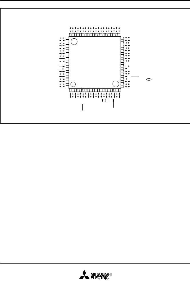
Fig. 1 M38867M8A-XXXHP, M38867E8AHP pin configuration
PIN CONFIGURATION (TOP VIEW)
P87/DQ7 |
|
|
|
|
|
|
|
|
65 |
|||
P86/DQ6 |
|
|
|
|
|
|
|
|
66 |
|||
P85/DQ5 |
|
|
|
|
|
|
|
|
67 |
|||
P84/DQ4 |
|
|
|
|
|
|
|
|
68 |
|||
P83/DQ3 |
|
|
|
|
|
|
|
|
69 |
|||
P82/DQ2 |
|
|
|
|
|
|
|
|
70 |
|||
P81/DQ1 |
|
|
|
|
|
|
71 |
|||||
P80/DQ0 |
|
|
|
|
|
|
72 |
|||||
VCC |
73 |
|||||||||||
VREF |
|
|
74 |
|||||||||
|
||||||||||||
AVSS |
|
|
|
|
75 |
|||||||
P67/AN7 |
|
|
|
|
|
76 |
||||||
P66/AN6 |
|
|
|
|
|
|
|
|
|
|
77 |
|
P65/AN5 |
|
|
|
|
|
|
|
|
|
|
78 |
|
P64/AN4 |
|
|
|
|
|
|
|
|
79 |
|||
P63/AN3 |
|
|
|
|
|
80 |
||||||
|
|
|
|
|
|
|
|
|
|
|
||
|
P30/PWM00 |
P31/PWM10 |
|
P32/ONW |
|
P33/RESETOUT |
P34/φ |
P35/SYNC |
|
P36/WR |
|
|
P37/RD |
P00/P3REF/AD0 |
P01/AD1 |
P02/AD2 |
P03/AD3 |
P04/AD4 |
P05/AD5 |
P06/AD6 |
|
P07/AD7 |
|
P10/AD8 |
|
P11/AD9 |
P12/AD10 |
P13/AD11 |
P14/AD12 |
P15/AD13 |
P16/AD14 |
P17/AD15 |
||||||||||||||||||||||||||||||||||||
|
|
|
|
|
|
|
|
|
||||||||||||||||||||||||||||||||||||||||||||||||||||||||||||
|
|
|
|
|
|
|
|
|
||||||||||||||||||||||||||||||||||||||||||||||||||||||||||||
|
|
|
|
|
|
|
|
|
||||||||||||||||||||||||||||||||||||||||||||||||||||||||||||
|
|
|
|
|
|
|
|
|
|
|
|
|
|
|
|
|
|
|
|
|
|
|
|
|
|
|
|
|
|
|
|
|
|
|
|
|
|
|
|
|
|
|
|
|
|
|
|
|
|
|
|
|
|
|
|
|
|
|
|
|
|
|
|
|
|
|
|
|
|
|
|
|
|
|
|
|
|
|
|
|
|
|
|
|
|
|
|
|
|
|
|
|
|
|
|
|
|
|
|
|
|
|
|
|
|
|
|
|
|
|
|
|
|
|
|
|
|
|
|
|
|
|
|
|
|
|
|
|
|
|
|
|
|
|
|
|
|
|
|
|
|
|
|
|
|
|
|
|
|
|
|
|
|
|
|
|
|
|
|
|
|
|
|
|
|
|
|
|
|
|
|
|
|
|
|
|
|
|
|
|
|
|
|
|
|
|
|
|
|
|
|
|
|
|
|
|
|
|
|
|
|
|
|
|
|
|
|
64 |
63 |
62 |
|
61 |
|
60 |
59 |
58 |
|
|
57 |
|
56 |
|
55 |
|
54 |
|
53 |
|
52 |
|
51 |
|
50 |
|
|
49 |
|
|
48 |
|
|
47 |
|
46 |
|
45 |
|
44 |
|
43 |
|
42 |
|
41 |
|
||||||||||||||||||||
|
|
|
|
|
|
|
|
|
|
|
|
|
|
|
|
|
|
|
|
|
|
|
|
|
|
|
|
|
|
|
|
|
|
|
|
|
|
|
|
|
|
|
|
|
|
|
|
|
|
|
|
|
|
|
M38867E8AFS |
|
|
|
|
|
|
|
|
|
||||
|
|
|
|
|
|
|
|
|
|
|
|
|
|
|
|
|
|
|
|
|
|
|
|
|
|
|
|
|
|
|
|
|
|
|
|
|
|
|
|
|
|
|
|
|
|
|
|
|
|
|
|
|
|
|
|
|
|
|
|
|
|
|
|
|
|
|
|
|
|
1 |
2 |
3 |
|
4 |
|
5 |
6 |
7 |
|
|
8 |
|
9 |
|
10 |
|
11 |
|
12 |
|
13 |
|
14 |
|
15 |
|
|
16 |
|
|
17 |
|
|
18 |
|
19 |
|
20 |
|
21 |
|
22 |
|
23 |
|
24 |
|
||||||||||||||||||||
|
|
|
|
|
|
|
|
|
|
|
|
|
|
|
|
|
|
|
|
|
|
|
|
|
|
|
|
|
|
|
|
|
|
|
|
|
|
|
|
|
|
|
|
|
|
|
|
|
|
|
|
|
|
|
|
|
|
|
|
|
|
|
|
|
|
|
||
|
|
|
|
|
|
|
|
|
|
|
|
|
|
|
|
|
|
|
|
|
|
|
|
|
|
|
|
|
|
|
|
|
|
|
|
|
|
|
|
|
|
|
|
|
|
|
|
|
|
|
|
|
|
|
|
|
|
|
|
|
|
|
|
|
|
|
|
|
|
|
|
|
|
P75/INT41 |
P74/INT31 |
|
|
|
P71/SOUT2 |
P70/SIN2 |
P57/DA2/PWM11 |
P56/DA1/PWM01 |
|
|
|
|
|
|
|
|
|
P47/SRDY1/S1 |
|
P45/TXD |
P44/RXD |
P43/INT1/OBF01 |
|||||||||||||||||||||||||||||||||||||||||
P62/AN2 |
P61/AN1 |
P60/AN0 |
P77/SCL |
P76/SDA |
|
P73/SRDY2/INT21 |
P72/SCLK2 |
P55/CNTR1 |
P54/CNTR0 |
|
P53/INT40/W |
|
P52/INT30/R |
|
P51/INT20/S0 |
P50/A0 |
P46/SCLK1/OBF10 |
|||||||||||||||||||||||||||||||||||||||||||||||||||
|
|
|
|
|||||||||||||||||||||||||||||||||||||||||||||||||||||||||||||||||
|
|
|
|
|||||||||||||||||||||||||||||||||||||||||||||||||||||||||||||||||
|
|
|
|
|
|
|
|
|
|
|
|
|
|
|
|
|
|
|
|
|
|
|
|
|
|
|
||||||||||||||||||||||||||||||||||||||||||
|
|
|
|
|
|
|
|
|
|
|
|
|
|
|
|
|
|
|
|
|
|
|
|
|
|
|
|
|
|
|
|
|
|
|
|
|
|
|
|
|
|
|
||||||||||||||||||||||||||
40 |
|
|
|
|
P20/DB0 |
|
||
39 |
|
|
|
|
P21/DB1 |
|
||
|
|
|
|
|
||||
|
|
|
|
|
||||
38 |
|
|
|
|
P22/DB2 |
|
||
37 |
|
|
|
|
P23/DB3 |
|
||
|
|
|
|
|
||||
|
|
|
|
|
||||
36 |
|
|
|
|
P24/DB4 |
|
||
35 |
|
|
|
|
P25/DB5 |
|
||
|
|
|
|
|
||||
34 |
|
|
|
|
P26/DB6 |
|
||
|
|
|
|
|
||||
33 |
|
|
|
|
P27/DB7 |
|
||
|
|
|
|
|
||||
|
|
|
|
|
||||
32 |
|
|
|
|
VSS |
|
||
31 |
|
|
|
|
XOUT |
|
||
30 |
|
|
|
|
XIN |
|
||
|
|
|
|
|
||||
|
|
|
|
|
||||
29 |
|
|
|
|
|
P40/XCOUT |
|
|
|
|
|
|
|
|
|||
28 |
|
|
|
|
|
P41/XCIN |
|
|
|
|
|
|
|||||
27 |
|
|
|
|
|
|
|
|
|
|
|
|
|
RESET |
VPP |
||
26 |
|
|
|
|
|
CNVSS |
||
|
|
|
|
|
||||
25 |
|
|
|
|
|
P42/INT0/OBF00 |
||
|
|
|
|
|
||||
|
|
|
|
|||||
Package type : 80D0
Note: The pin number and the position of the function pin may change by the kind of package.
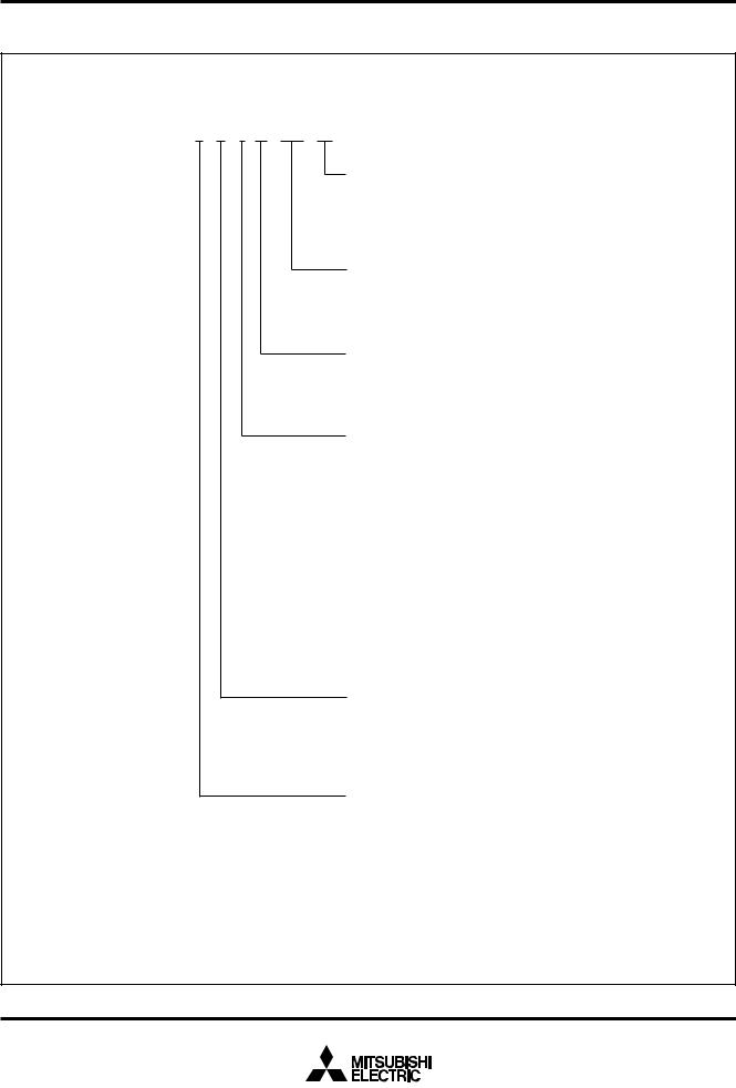
Fig. 2 M38867E8AFS pin configuration
2
MITSUBISHI MICROCOMPUTERS
3886 Group
SINGLE-CHIP 8-BIT CMOS MICROCOMPUTER
PIN CONFIGURATION (TOP VIEW)
|
|
|
P32 |
P33 |
P34 |
P35 |
P36 |
P37 |
P0/P30REF |
P01 |
P02 |
P03 |
P04 |
P05 |
P06 |
P07 |
P10 |
P11 |
P12 |
P13 |
P14 |
P15 |
|
|
|
||||||||||||||||||||
|
|
|
|
|
|
|
|
|
|
|
|
|
|
|
|
|
|
|
|
|
|
|
|
|
|
|
|
|
|
|
|
|
|
|
|
|
|
|
|
|
|
|
|
|
|
|
|
|
|
|
|
|
|
|
|
|
|
|
|
|
|
|
|
|
|
|
|
|
|
|
|
|
|
|
|
|
|
|
|
|
|
|
|
|
|
|
|
|
|
|
|
|
|
|
60 |
59 |
58 |
57 |
56 |
55 |
54 |
53 |
52 |
51 |
50 |
49 |
48 |
47 |
46 |
45 |
44 |
43 |
42 |
41 |
|
|
|
||||||||||||||||||||
P31/PWM10 |
|
61 |
|
|
|
|
|
|
|
|
|
|
|
|
|
|
|
|
|
|
|
|
|
|
|
|
|
|
|
|
|
|
|
|
|
|
|
|
|
|
40 |
|
P16 |
|
|
|
|
|
|
|
|
|
|
|
|
|
|
|
|
|
|
|
|
|
|
|
|
|
|
|
|
|
|
|
|
|
|
|
|
|
|
|
|
|
|
|
|||||
P30/PWM00 |
|
62 |
|
|
|
|
|
|
|
|
|
|
|
|
|
|
|
|
|
|
|
|
|
|
|
|
|
|
|
|
|
|
|
|
|
|
|
|
|
|
39 |
|
P17 |
|
|
|
|
|
|
|
|
|
|
|
|
|
|
|
|
|
|
|
|
|
|
|
|
|
|
|
|
|
|
|
|
|
|
|
|
|
|
|
|
|
|
|
|||||
P87/DQ7 |
63 |
|
|
|
|
|
|
|
|
|
|
|
|
|
|
|
|
|
|
|
|
|
|
|
|
|
|
|
|
|
|
|
|
|
|
|
|
|
|
38 |
|
P20 |
|
||
P86/DQ6 |
64 |
|
|
|
|
|
|
|
|
|
|
|
|
|
|
|
|
|
|
|
|
|
|
|
|
|
|
|
|
|
|
|
|
|
|
|
|
|
|
37 |
|
P21 |
|
||
P85/DQ5 |
65 |
|
|
|
|
|
|
|
|
|
|
|
|
|
|
|
|
|
|
|
|
|
|
|
|
|
|
|
|
|
|
|
|
|
|
|
|
|
|
36 |
|
P22 |
|
||
P84/DQ4 |
66 |
|
|
|
|
|
|
|
|
|
|
|
|
|
|
|
|
|
|
|
|
|
|
|
|
|
|
|
|
|
|
|
|
|
|
|
|
|
|
35 |
|
P23 |
|
||
P83/DQ3 |
67 |
|
|
|
|
|
|
|
|
|
|
|
|
|
|
|
|
|
|
|
|
|
|
|
|
|
|
|
|
|
|
|
|
|
|
|
|
|
|
34 |
|
P24 |
|
||
P82/DQ2 |
68 |
|
|
|
|
|
|
|
|
|
|
|
|
|
|
|
|
|
|
|
|
|
|
|
|
|
|
|
|
|
|
|
|
|
|
|
|
|
|
33 |
|
P25 |
|
||
P80/DQ0 |
70 |
M38869MFA-XXXGP/HP 31 |
|
P27 |
|
||||||||||||||||||||||||||||||||||||||||
P81/DQ1 |
69 |
|
|
|
|
|
|
|
|
|
|
|
|
|
|
|
|
|
|
|
|
|
|
|
|
|
|
|
|
|
|
|
|
|
|
|
|
|
|
32 |
|
P26 |
|
||
VCC |
71 |
|
|
|
|
|
M38869FFAGP/HP |
|
|
30 |
|
VSS |
|
||||||||||||||||||||||||||||||||
VREF |
72 |
|
|
|
|
|
|
|
29 |
|
XOUT |
|
|||||||||||||||||||||||||||||||||
AVSS |
73 |
|
|
|
|
|
|
|
|
|
|
|
|
|
|
|
|
|
|
|
|
|
|
|
|
|
|
|
|
|
|
|
|
|
|
|
|
|
|
28 |
|
XIN |
|
||
P67/AN7 |
74 |
|
|
|
|
|
|
|
|
|
|
|
|
|
|
|
|
|
|
|
|
|
|
|
|
|
|
|
|
|
|
|
|
|
|
|
|
|
|
27 |
|
P40/XCOUT |
|
||
P66/AN6 |
75 |
|
|
|
|
|
|
|
|
|
|
|
|
|
|
|
|
|
|
|
|
|
|
|
|
|
|
|
|
|
|
|
|
|
|
|
|
|
|
26 |
|
P41/XCIN |
|
||
P65/AN5 |
76 |
|
|
|
|
|
|
|
|
|
|
|
|
|
|
|
|
|
|
|
|
|
|
|
|
|
|
|
|
|
|
|
|
|
|
|
|
|
|
25 |
|
RESET |
|
||
P64/AN4 |
77 |
|
|
|
|
|
|
|
|
|
|
|
|
|
|
|
|
|
|
|
|
|
|
|
|
|
|
|
|
|
|
|
|
|
|
|
|
|
|
24 |
|
CNVSS |
VPP |
||
P63/AN3 |
78 |
|
|
|
|
|
|
|
|
|
|
|
|
|
|
|
|
|
|
|
|
|
|
|
|
|
|
|
|
|
|
|
|
|
|
|
|
|
|
23 |
|
P42/INT0/OBF00 |
|
||
P62/AN2 |
|
79 |
|
|
|
|
|
|
|
|
|
|
|
|
|
|
|
|
|
|
|
|
|
|
|
|
|
|
|
|
|
|
|
|
|
|
|
|
|
|
22 |
|
P43/INT1/OBF01 |
|
|
|
|
|
|
|
|
|
|
|
|
|
|
|
|
|
|
|
|
|
|
|
|
|
|
|
|
|
|
|
|
|
|
|
|
|
|
|
|
|
|
|
|||||
P61/AN1 |
|
80 |
|
|
|
|
|
|
|
|
|
|
|
|
|
|
|
|
|
|
|
|
|
|
|
|
|
|
|
|
|
|
|
|
|
|
|
|
|
|
21 |
|
P44/RXD |
|
|
|
|
|
|
|
|
|
|
|
|
|
|
|
|
|
|
|
|
|
|
|
|
|
|
|
|
|
|
|
|
|
|
|
|
|
|
|
|
|
|
|
|||||
|
|
|
1 |
2 |
3 |
4 |
5 |
6 |
7 |
8 |
9 |
10 |
11 |
12 |
13 |
14 |
15 |
16 |
17 |
18 |
19 |
20 |
|
|
|
||||||||||||||||||||
P6/AN00 |
P7/S7CL |
P7/S6DA |
P7/INT541 |
P7/INT431 |
P7/S/INT3RDY221 |
P7/S2CLK2 |
P7/S1OUT2 |
P7/S0IN2 |
P5/DA/PWM7211 |
P5/DA/PWM6101 |
P5/CNTR51 |
P5/CNTR40 |
P5/INT/W340 |
P5/INT/R230 |
P5/INT/S1200 |
P5/A00 |
P4/S/S7RDY11 |
P4/S/OBF6CLK110 |
P4/TD5X |
Package type : 80P6S-A/80P6Q-A
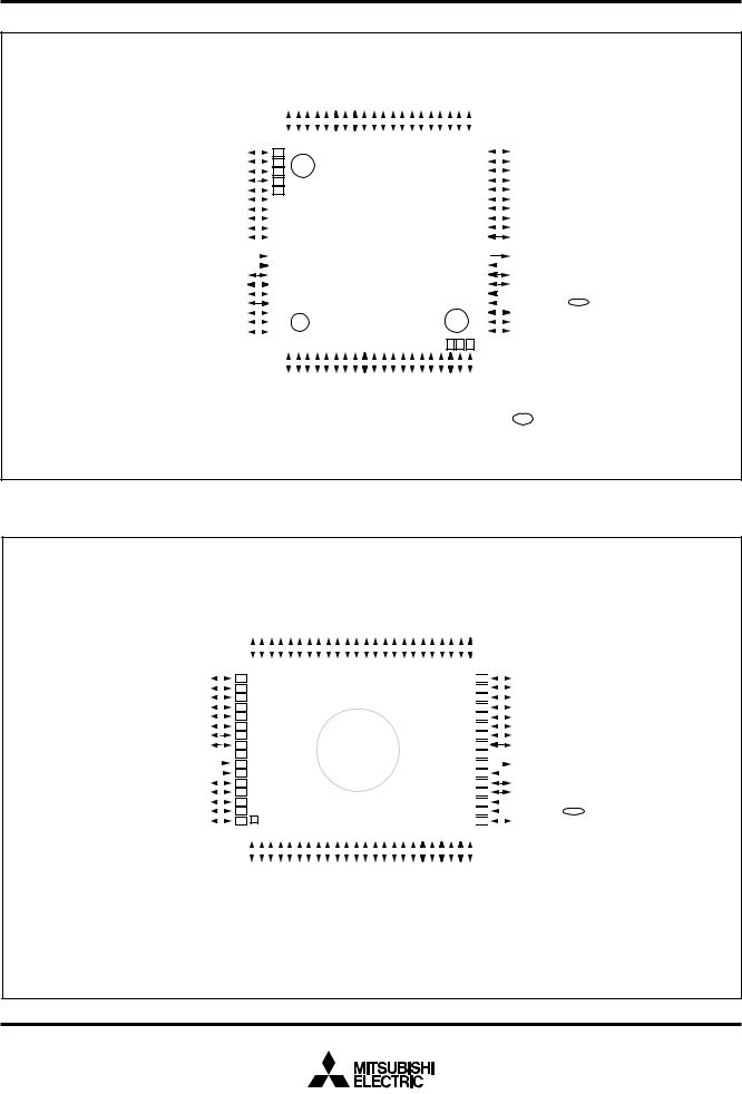
Fig. 3 M38869MFA-XXXGP/HP, M38869FFAGP/HP pin configuration
 : Flash memory version
Note: The pin number and the position of the function pin may change by the kind of package.
3

4 |
diagramblockFunctional4.Fig |
FUNCTIONAL BLOCK DIAGRAM (Package : 80P6Q-A, 80P6S-A) |
|
|
|
|
|
|
|
|
|
|
BLOCKFUNCTIONAL |
|
|
|||||||||||||||||
|
|
|
|
|
|
|
|
|
|
|
|
|
|
|
||||||||||||||||||
|
|
Main-clock |
Main-clock |
|
|
|
|
|
|
|
|
|
|
|
|
|
|
Reset input |
|
|
|
|
|
|
|
|
|
|
|
|
||
|
|
input |
output |
|
|
|
|
|
|
|
|
|
|
|
|
|
|
|
|
|
|
|
|
|
|
|
|
|
|
|||
|
|
|
|
|
|
|
|
|
|
|
|
|
|
|
|
|
CNVSS |
|
|
|
|
|
|
|
|
|
|
|||||
|
|
XIN |
XOUT |
|
|
|
|
|
|
|
|
|
|
|
|
|
VSS |
VCC |
|
RESET |
|
|
|
|
|
|
|
|
|
|
||
|
|
28 |
29 |
|
|
|
|
|
|
|
|
|
|
|
|
|
30 |
71 |
|
25 |
24 |
|
|
|
|
|
|
|
|
|
|
|
|
|
|
|
|
Sub-clock Sub-clock |
|
|
|
|
|
|
|
|
|
|
|
|
|
|
|
|
|
|
|
|
|
||||||
|
|
|
|
|
input |
|
|
output |
|
|
|
|
|
|
|
|
|
|
|
|
|
|
|
|
|
|
|
|
|
|||
|
|
|
|
|
XCIN |
|
|
XCOUT |
|
|
|
|
|
|
|
|
|
|
|
|
|
|
|
|
|
|
|
|
|
|||
|
|
|
Clock generating circuit |
|
|
|
|
|
|
|
|
|
|
|
|
|
|
Timer |
1( 8 ) |
|
|
|
|
|||||||||
|
|
|
|
|
|
|
|
|
|
|
|
|
|
|
|
|
|
|
|
|
|
|
|
|
|
|
|
|
|
|||
|
|
|
|
|
|
|
|
|
|
|
|
|
|
|
|
|
|
|
|
|
|
Prescaler |
12(8) |
|
|
Timer |
2( 8 ) |
|
|
|
|
|
|
|
|
|
|
|
|
|
|
|
|
|
|
|
|
|
|
|
|
|
|
|
Prescaler |
X(8) |
|
|
Timer |
X( 8 ) |
|
|
|
|
|
|
|
Watchdog |
|
|
|
|
|
|
|
|
|
|
|
|
|
|
|
|
Prescaler |
Y(8) |
|
|
Timer |
Y( 8 ) |
|
|
|
|
||||
|
|
|
|
|
|
Reset |
|
|
|
|
|
|
|
|
|
|
|
|
|
|
|
|
|
|
|
|
||||||
|
|
|
timer |
|
|
|
|
|
|
|
|
|
|
|
|
|
|
|
|
|
|
|
|
|
|
|
|
|
|
|||
|
|
|
|
|
|
|
|
|
|
|
|
|
|
|
|
|
|
|
|
|
|
|
|
|
|
|
|
|
|
|
|
|
|
|
|
|
2 |
|
|
|
|
|
|
SI/O2(8) |
|
|
|
|
INT20, |
|
|
|
|
PWM01 |
|
|
PWM11 |
|
-SINGLE |
|
|
||||
|
|
|
I |
|
C |
|
|
|
|
|
converter |
D-A |
D-A |
SI/O1(8) |
Comparator |
|
|
PWM0(14) |
PWM1(14) |
|
|
|
||||||||||
|
|
|
|
|
|
|
|
|
|
|
|
|
|
(10) |
|
converter 2 |
converter |
|
|
|
|
|
|
|
|
|
|
|
|
|
|
|
|
|
|
SCL SDA |
|
|
|
|
|
|
|
|
|
|
(8) |
1(8) |
|
|
|
|
|
|
|
|
|
|
|
|
|
|
|
||
|
|
|
|
|
|
|
|
|
|
|
|
|
|
|
|
|
|
|
|
PWM00, |
|
|
PWM10, |
|
|
|
|
|||||
|
|
|
|
|
|
|
|
|
|
|
|
|
|
|
|
|
|
|
|
|
|
|
|
|
|
|
|
|
||||
|
|
|
Bus interface |
|
|
|
|
|
|
|
INT21, |
|
|
|
|
INT30, |
|
XCOUT |
Key-on |
|
|
|
|
|
|
|
MICROCOMPUTERCMOSBIT-8CHIP |
|
MICROCOMPUTERSMITSUBISHI |
|||
|
|
|
DQ0 |
|
|
|
|
|
|
|
|
|
|
|
|
|
XCIN |
wake-up |
|
|
|
|
|
|
|
Group3886 |
||||||
|
|
|
|
|
|
|
|
|
|
|
INT31, |
|
|
|
|
INT40 |
INT0, |
|
|
|
|
|
|
|
||||||||
|
|
|
|
|
|
|
|
|
|
|
|
|
|
|
|
|
|
|
|
|
|
|
|
|
||||||||
|
|
|
|
|
|
|
|
|
|
|
|
|
|
|
|
|
|
|
|
|
|
|
|
|
|
|
|
|||||
|
|
|
to |
|
|
|
|
|
|
|
|
|
INT41 |
|
|
|
|
|
INT1 |
|
|
|
|
|
|
|
|
|
|
|
|
|
|
|
|
DQ7 |
|
|
|
|
|
|
|
|
|
|
|
|
|
|
|
|
|
|
|
|
|
|
|
|
|
|
|
|
|
|
|
P8(8) |
|
|
|
P7(8) |
|
|
|
|
|
P6(8) |
P5(8) |
|
P4(8) |
P3(8) |
|
P2(8) |
|
|
P1(8) |
|
|
P0(8) |
|
|
|
|||||
|
|
|
|
|
|
|
|
|
|
|
|
|
|
|
|
|
|
|
|
|
|
|
|
|
|
|
|
|
|
P3REF |
|
|
|
|
63 64 65 66 67 68 69 70 |
2 |
3 |
4 |
5 |
6 |
7 |
8 |
9 |
72 73 |
74 75 76 77 78 79 80 1 |
10 11 12 13 14 15 16 17 |
|
18 19 20 21 22 23 26 27 |
55 56 57 58 59 60 61 62 |
31 32 33 34 35 36 37 38 |
39 40 41 42 43 44 45 46 |
47 48 49 50 51 52 53 54 |
|
|
|
||||||||||
|
|
I/O port P8 |
|
|
I/O port P7 |
|
|
|
|
I/O port P6 |
I/O port P5 |
|
I/O port P4 |
I/O port P3 |
I/O port P2 |
|
I/O port P1 |
|
I/O port P0 |
|
|
|
||||||||||
|
|
|
|
|
|
|
|
|
|
|
|
|
VREF |
|
|
|
|
|
|
|
|
|
|
|
|
|
|
|
|
|
|
|
|
|
|
|
|
|
|
|
|
|
|
|
|
|
AVSS |
|
|
|
|
|
|
|
|
|
|
|
|
|
|
|
|
|
|

MITSUBISHI MICROCOMPUTERS
3886 Group
SINGLE-CHIP 8-BIT CMOS MICROCOMPUTER
PIN DESCRIPTION
Table 1 Pin description (1)
|
Pin |
Name |
Functions |
|
|
|
|
Function except a port function |
|||||
|
|
|
|
|
|
|
|
|
|
|
|
|
|
|
VCC, VSS |
Power source |
•Apply voltage of 2.7 V – 5.5 V to Vcc, and 0 V to Vss. |
|
||
|
•In the flash memory version, apply voltage of 4.0 V – 5.5 V to Vcc, and 0 V to Vss |
|||||
|
|
|
|
|||
|
|
|
|
•This pin controls the operation mode of the chip. |
|
|
|
|
|
|
•Normally connected to VSS. |
|
|
|
CNVSS |
CNVSS input |
•If this pin is connected to Vcc, the internal ROM is inhibited and an external memory is accessed. |
|||
|
|
|
|
•In the flash memory version, connected to VSS. |
|
|
|
|
|
|
•In the EPROM version or the flash memory version, this pin functions as the VPP power source input pin. |
||
|
|
|
|
|
|
|
|
VREF |
Reference voltage |
•Reference voltage input pin for A-D and D-A converters. |
|
||
|
|
|
|
|
|
|
|
AVSS |
Analog power source |
•Analog power source input pin for A-D and D-A converters. |
|||
|
•Connect to VSS. |
|
||||
|
|
|
|
|
||
|
|
|
|
|
|
|
|
|
Reset input |
•Reset input pin for active “L”. |
|
||
|
RESET |
|
|
|||
|
XIN |
Clock input |
•Input and output pins for the clock generating circuit. |
|
||
|
•Connect a ceramic resonator or quartz-crystal oscillator between the XIN and XOUT pins to set |
|||||
|
|
|
|
|||
|
|
|
|
the oscillation frequency. |
|
|
|
|
|
|
|
||
|
XOUT |
Clock output |
•When an external clock is used, connect the clock source to the XIN pin and leave the XOUT |
|||
|
|
|
|
pin open. |
|
|
|
P00/P3REF |
|
•8-bit CMOS I/O port. |
•Comparator reference power source |
||
|
|
•I/O direction register allows each pin to be individually |
input pin |
|||
|
|
|
I/O port P0 |
programmed as either input or output. |
|
|
|
|
|
|
|||
|
|
|
•When the external memory is used, these pins are used as the address bus. |
|||
|
|
|
|
|||
|
P01–P07 |
|
•CMOS compatible input level. |
|
||
|
|
|
|
•CMOS 3-state output structure or N-channel open-drain output structure. |
||
|
|
|
|
|
|
|
|
|
|
|
•8-bit CMOS I/O port. |
|
|
|
|
|
|
•I/O direction register allows each pin to be individually programmed as either input or output. |
||
|
P10–P17 |
I/O port P1 |
•When the external memory is used, these pins are used as the address bus. |
|||
|
|
|
|
•CMOS compatible input level. |
|
|
|
|
|
|
•CMOS 3-state output structure or N-channel open-drain output structure. |
||
|
|
|
|
|
|
|
|
|
|
|
•8-bit CMOS I/O port. |
|
|
|
|
|
|
•I/O direction register allows each pin to be individually programmed as either input or output. |
||
|
P20–P27 |
I/O port P2 |
•When the external memory is used, these pins are used as the data bus. |
|||
|
•CMOS compatible input level. |
|
||||
|
|
|
|
|
||
|
|
|
|
•CMOS 3-state output structure. |
|
|
|
|
|
|
•P24 to P27 (4 bits) are enabled to output large current for LED drive (only in single-chip mode). |
||
|
|
|
|
|
|
|
|
|
|
|
•8-bit CMOS I/O port. |
•Key-on wake-up input pin |
|
|
|
|
|
|
|
|
|
P30/PWM00 |
|
•I/O direction register allows each pin to be individually |
•Comparator input pin |
||
|
|
programmed as either input or output. |
||||
|
|
•PWM output pin |
||||
|
P31/PWM10 |
|
||||
|
|
•When the external memory is used, these pins are |
||||
|
|
|
|
|
||
|
|
|
I/O port P3 |
used as the control bus. |
|
|
|
|
|
•CMOS compatible input level. |
|
||
|
|
|
•Key-on wake-up input pin |
|||
|
|
|
|
|||
|
|
|
|
•CMOS 3-state output structure. |
•Comparator input pin |
|
|
P32–P37 |
|
•These pins function as key-on wake-up and compara- |
|
||
|
|
|
|
tor input. |
|
|
|
|
|
|
•These pins are enabled to control pull-up. |
|
|
|
|
|
|
|
|
|
5

MITSUBISHI MICROCOMPUTERS
3886 Group
SINGLE-CHIP 8-BIT CMOS MICROCOMPUTER
Table 2 Pin description (2)
Pin |
Name |
Functions |
|
||||
Function except a port function |
|||||||
|
|
|
|
|
|
||
|
|
|
|
|
|
|
|
P40/XCOUT |
|
•8-bit I/O port with the same function as port P0. |
•Sub-clock generating circuit I/O |
||||
|
<Input level> |
||||||
|
pins |
||||||
P41/XCIN |
|
||||||
|
P40, P41 : CMOS input level |
(Connect a resonator.) |
|||||
|
|
|
|
|
|||
|
|
|
|
|
P42–P46 : CMOS compatible input level or TTL in- |
|
|
|
|
|
|
|
|
||
P42/INT0 |
|
put level |
|
||||
|
P47 : CMOS compatible input level or TTL input |
•Interrupt input pins |
|||||
/OBF00 |
|
||||||
P43/INT1 |
I/O port P4 |
level in the bus interface function |
•Bus interface function pins |
||||
<Output structure> |
|
||||||
/OBF01 |
|
||||||
|
|
||||||
|
|
|
|
|
P40, P41, P47 : CMOS 3-state output structure |
|
|
|
|
|
|
|
|
||
P44/RxD |
|
P42–P46 : CMOS 3-state output structure or N- |
|
||||
|
channel open-drain output structure |
•Serial I/O1 function pins |
|||||
P45/TxD |
|
||||||
|
•Regardless of input or output port, P42 to P46 can |
|
|||||
|
|
|
|
|
|
||
|
|
|
|
|
be input every pin level. |
|
|
P46/SCLK1 |
|
•When P42 and P43 are used as output port, the |
|
||||
/OBF10 |
|
•Serial I/O1 function pins |
|||||
|
function which makes P42 and P43 clear to “0” |
||||||
|
|
|
|
|
|
||
P47/SRDY1 |
|
|
|
when the host CPU reads the output data bus |
•Bus interface function pins |
||
/S1 |
|
buffer 0 can be added. |
|
||||
P50/A0 |
|
•8-bit I/O port with the same function as port P0. |
•Bus interface function pins |
||||
|
|
|
•CMOS compatible input level. |
|
|||
P51/INT20 |
|
|
|||||
/S0 |
|
•CMOS 3-state output structure. |
•Interrupt input pins |
||||
P52/INT30 |
|
•P50 to P53 can be switched between CMOS com- |
|||||
/R |
|
patible input level or TTL input level in the bus |
•Bus interface function pins |
||||
P53/INT40 |
I/O port P5 |
interface function. |
|
||||
/W |
|
|
|||||
|
|
|
|||||
P54/CNTR0 |
|
|
•Timer X, timer Y function pins |
||||
P55/CNTR1 |
|
|
|||||
|
|
|
|||||
|
|
|
|
|
|||
P56/DA1 |
|
|
•D-A converter output pin |
||||
/PWM01 |
|
|
|||||
P57/DA2 |
|
|
•PWM output pin |
||||
/PWM11 |
|
|
|
||||
|
|
|
|
|
|
|
|
|
|
|
|
|
•8-bit I/O port with the same function as port P0. |
|
|
P60/AN0– |
I/O port P6 |
•CMOS compatible input level. |
•A-D converter output pin |
||||
P67/AN7 |
|
•CMOS 3-state output structure. |
|
||||
|
|
|
|
|
|
||
P70/SIN2 |
|
•8-bit I/O port with the same function as port P0. |
|
||||
P71/SOUT2 |
|
P70–P75 : CMOS compatible input level or TTL in- |
•Serial I/O2 function pin |
||||
P72/SCLK2 |
|
put level |
|
||||
|
|
|
|
|
P76, P77 : CMOS compatible input level or |
•Serial I/O2 function pin |
|
P73/SRDY2 |
|
||||||
/INT21 |
I/O port P7 |
SMBUS input level in the I2C-BUS inter- |
•Interrupt input pin |
||||
P74/INT31 |
|
face function, N-channel open-drain |
|
||||
|
|
||||||
|
output structure |
•Interrupt input pin |
|||||
P75/INT41 |
|
||||||
|
•Regardless of input or output port, P70 to P75 can |
|
|||||
|
|
|
|
|
|
||
P76/SDA |
|
be input every pin level. |
•I2C-BUS interface function pin |
||||
P77/SCL |
|
|
|||||
|
|
|
|||||
|
|
|
|
|
•8-bit I/O port with the same function as port P0. |
|
|
P80/DQ0– |
|
•CMOS compatible input level. |
|
||||
I/O port P8 |
•CMOS 3-state output structure. |
•Bus interface function pin |
|||||
P87/DQ7 |
|||||||
|
|
|
|
|
•CMOS compatible input level or TTL input level in |
|
|
|
|
|
|
|
the bus interface function. |
|
|
|
|
|
|
|
|
|
|
6
MITSUBISHI MICROCOMPUTERS
3886 Group
SINGLE-CHIP 8-BIT CMOS MICROCOMPUTER
PART NUMBERING
Product name |
M3886 7 M 8 A- XXX HP |
Package type
HP : 80P6Q-A
GP : 80P6S-A
FS : 80D0
ROM number
Omitted in the one time PROM version shipped in blank, the EPROM version and the flash memory version.
A– : High-speed version
– is omitted in the One Time PROM version shipped in blank, the EPROM version and the flash memory version.
ROM/PROM size 1: 4096 bytes
2: 8192 bytes 3: 12288 bytes 4: 16384 bytes 5: 20480 bytes 6: 24576 bytes 7: 28672 bytes 8: 32768 bytes
The first 128 bytes and the last 2 bytes of ROM are reserved areas ; they cannot be used.
However, they can be programmed or erased in the EPROM version and the flash memory version, so that the users can use them.
Memory type
M : Mask ROM version
E: EPROM or One Time PROM version
F: Flash memory version
RAM size |
|
|
0 : 192 bytes |
5 |
: 768 bytes |
1 : 256 bytes |
6 |
: 896 bytes |
2 : 384 bytes |
7 |
: 1024 bytes |
3 : 512 bytes |
8 |
: 1536 bytes |
4 : 640 bytes |
9 |
: 2048 bytes |
Fig. 5 Part numbering
7
MITSUBISHI MICROCOMPUTERS
3886 Group
SINGLE-CHIP 8-BIT CMOS MICROCOMPUTER
GROUP EXPANSION
Mitsubishi plans to expand the 3886 group as follows.
Memory Type
Support for mask ROM, One Time PROM, EPROM and flash memory version.
Packages
80P6Q-A |
.................................. 0.5 mm-pitch plastic molded LQFP |
80P6S-A |
................................... 0.65mm pitch plastic molded QFP |
80D0 ....................... |
0.8 mm - pitch ceramic LCC (EPROM version) |
The pin number and the position of the function pin may change by the kind of package.
Memory Size
ROM size ........................................................... 32 K to 60 K bytes
RAM size .......................................................... 1024 to 2048 bytes
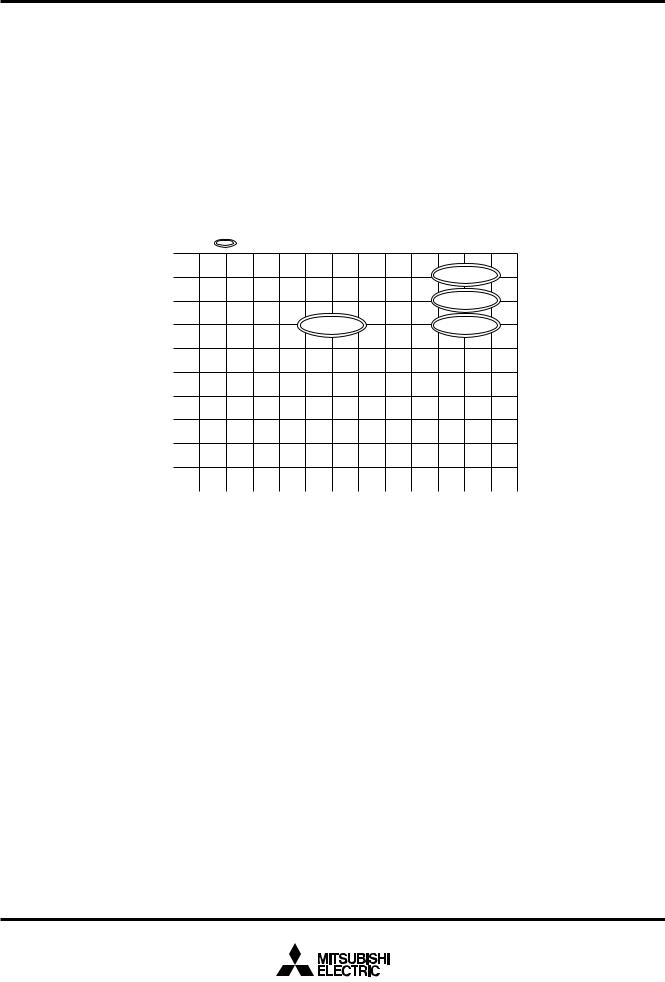
|
Memory Expansion |
|
|
|
|
|
|
|
|
|
|
|
|
|
|
|
||
|
|
ROM size (bytes) |
|
|
|
|
|
|
|
|
|
|
|
|
|
|
||
|
|
|
|
: Mass production |
|
|
|
|
|
|
|
|
|
|
||||
|
|
ROM |
|
|
|
|
|
|
|
|
|
|
|
|
|
|
|
|
|
|
external |
|
|
|
|
|
|
|
|
|
|
|
|
|
|
|
|
|
|
60K |
|
|
|
|
|
|
|
|
|
|
|
M38869FFA/MFA |
|
|
||
|
|
48K |
|
|
|
|
|
|
|
|
|
|
|
M38869MCA |
|
|
|
|
|
|
32K |
|
|
|
|
|
|
M38867E8A/M8A |
|
|
|
M38869M8A |
|
|
|
||
|
|
28K |
|
|
|
|
|
|
|
|
|
|
|
|
|
|
|
|
|
|
24K |
|
|
|
|
|
|
|
|
|
|
|
|
|
|
|
|
|
|
20K |
|
|
|
|
|
|
|
|
|
|
|
|
|
|
|
|
|
|
16K |
|
|
|
|
|
|
|
|
|
|
|
|
|
|
|
|
|
|
12K |
|
|
|
|
|
|
|
|
|
|
|
|
|
|
|
|
|
|
8K |
|
|
|
|
|
|
|
|
|
|
|
|
|
|
|
|
|
|
|
|
|
|
|
|
|
|
|
|
|
|
|
|
|
|
|
|
|
|
384 |
512 |
640 |
768 |
|
896 |
1024 |
1152 |
1280 |
1408 |
1536 |
2048 |
3072 |
4032 |
||
|
|
|
|
|
|
|
|
|
|
RAM size (bytes) |
|
|
|
|
|
|
|
|
|
|
|
|
|
|
|
|
|
|
|
|
|
|
|
|
|
|
|
|
Fig. 6 Memory expansion plan |
|
|
|
|
|
|
|
|
|
|
|
|
|
|
|
||
Currently products are listed below. |
|
|
|
|
|
|
|
|
|
|
|
|
|
|
|
|||
Table 3 Support products |
|
|
|
|
|
|
|
|
|
|
|
|
|
|
As of Jan. 2000 |
|||
|
Product name |
(P) ROM size (bytes) |
|
RAM size (bytes) |
Package |
|
|
|
|
Remarks |
||||||||
|
ROM size for User in ( |
) |
|
|
|
|
|
|||||||||||
|
|
|
|
|
|
|
|
|
|
|
|
|
|
|
|
|||
|
|
|
|
|
|
|
|
|
|
|
|
|
|
|
|
|||
|
M38867M8A-XXXHP |
|
|
|
|
|
|
|
|
|
|
|
Mask ROM version |
|
|
|||
|
M38867E8A-XXXHP |
|
|
|
|
|
1024 |
|
|
80P6Q-A |
One Time PROM version |
|||||||
|
M38867E8AHP |
32768 (32638) |
|
|
|
|
|
|
|
|
|
One Time PROM version (blank) |
||||||
|
M38867E8AFS |
|
|
|
|
|
|
|
80D0 |
EPROM version |
|
|
||||||
|
|
|
|
|
|
|
|
|
|
|
|
|||||||
|
M38869M8A-XXXHP |
|
|
|
|
|
|
|
|
|
80P6Q-A |
|
|
|
|
|
|
|
|
M38869M8A-XXXGP |
|
|
|
|
|
|
|
|
|
80P6S-A |
|
|
|
|
|
|
|
|
M38869MCA-XXXHP |
49152 (19022) |
|
|
|
|
|
|
|
80P6Q-A |
Mask ROM version |
|
|
|||||
|
M38869MCA-XXXGP |
|
|
|
2048 |
|
|
80P6S-A |
|
|
||||||||
|
|
|
|
|
|
|
|
|
|
|
|
|
|
|||||
|
M38869MFA-XXXHP |
|
|
|
|
|
|
|
|
|
80P6Q-A |
|
|
|
|
|
|
|
|
|
|
|
|
|
|
|
|
|
|
|
|
|
|
|
|
|
|
|
M38869MFA-XXXGP |
61440 (61310) |
|
|
|
|
|
|
|
80P6S-A |
|
|
|
|
|
|
||
|
|
|
|
|
|
|
|
|
|
|
|
|
|
|
|
|
||
|
M38869FFAHP |
|
|
|
|
|
|
|
80P6Q-A |
Flash memory version |
||||||||
|
|
|
|
|
|
|
|
|
|
|||||||||
|
|
|
|
|
|
|
|
|
|
|
|
|
||||||
|
M38869FFAGP |
|
|
|
|
|
|
|
|
|
80P6S-A |
|||||||
|
|
|
|
|
|
|
|
|
|
|
|
|
|
|
|
|||
|
|
|
|
|
|
|
|
|
|
|
|
|
|
|
|
|
|
|
8

MITSUBISHI MICROCOMPUTERS
3886 Group
SINGLE-CHIP 8-BIT CMOS MICROCOMPUTER
FUNCTIONAL DESCRIPTION
CENTRAL PROCESSING UNIT (CPU)
The 3886 group uses the standard 740 Family instruction set. Refer to the table of 740 Family addressing modes and machine instructions or the 740 Family Software Manual for details on the instruction set.
Machine-resident 740 Family instructions are as follows:
The FST and SLW instructions cannot be used.
The STP, WIT, MUL, and DIV instructions can be used.
[CPU Mode Register (CPUM)] 003B16
The CPU mode register contains the stack page selection bit, the processor mode bits specifying the chip operation mode, etc.
The CPU mode register is allocated at address 003B16.
b7 |
|
b0 |
|
|
||||||||||||||||
|
|
|
|
|
|
|
|
|
|
|
|
|
|
|
|
CPU mode register |
||||
|
|
|
|
|
|
|
|
|
|
|
|
|
|
|
|
(CPUM : address 003B16) |
||||
|
|
|
|
|
|
|
|
|
|
|
|
|
|
|
|
|
|
Processor mode bits |
||
|
|
|
|
|
|
|
|
|
|
|
|
|
|
|
|
|
||||
|
|
|
|
|
|
|
|
|
|
|
|
|
|
|
|
|
|
b1 b0 |
|
|
|
|
|
|
|
|
|
|
|
|
|
|
|
0 |
0 |
: Single-chip mode |
|||||
|
|
|
|
|
|
|
|
|
|
|
|
|
0 |
1 |
: Memory expansion mode (Note) |
|||||
|
|
|
|
|
|
|
|
|
|
|
|
|
1 |
0 |
: Microprocessor mode (Note) |
|||||
|
|
|
|
|
|
|
|
|
|
|
|
|
1 |
1 |
: Not available |
|||||
|
|
|
|
|
|
|
|
|
|
|
|
|
|
|
|
|
|
Stack page selection bit |
||
|
|
|
|
|
|
|
|
|
|
|
|
|
0 |
: 0 page |
||||||
|
|
|
|
|
|
|
|
|
|
|
|
|
1 |
: 1 page |
||||||
|
|
|
|
|
|
|
|
|
|
|
|
|
|
|
|
|
|
Reserved |
||
|
|
|
|
|
|
|
|
|
|
|
|
|
|
|
|
|
|
|||
|
|
|
|
|
|
|
|
|
|
|
|
|
|
|
|
|
|
(Do not write “0” to this bit when using |
||
|
|
|
|
|
|
|
|
|
|
|
|
|
|
|
|
|
|
XCIN–XCOUT oscillation function.) |
||
|
|
|
|
|
|
|
|
|
|
|
|
|
|
|
|
|
|
Port XC switch bit |
||
|
|
|
|
|
|
|
|
|
|
|
|
|
|
|
|
|
|
|||
|
|
|
|
|
|
|
|
|
|
|
|
|
|
|
|
|
|
0 : I/O port function (stop oscillating) |
||
|
|
|
|
|
|
|
|
|
|
|
|
|
|
|
|
|
|
1 : XCIN–XCOUT oscillating function |
||
|
|
|
|
|
|
|
|
|
|
|
|
|
|
|
|
|
|
Main clock (XIN–XOUT) stop bit |
||
|
|
|
|
|
|
|
|
|
|
|
|
|
|
|
|
|
|
|||
|
|
|
|
|
|
|
|
|
|
|
|
|
|
|
|
|
|
0 : Oscillating |
||
|
|
|
|
|
|
|
|
|
|
|
|
|
|
|
|
|
|
1 : Stopped |
||
|
|
|
|
|
|
|
|
|
|
|
|
|
|
|
|
|
|
Main clock division ratio selection bits |
||
|
|
|
|
|
|
|
|
|
|
|
|
|
|
|
|
|
|
|||
|
|
|
|
|
|
|
|
|
|
|
|
|
|
|
|
|
|
b7 b6 |
: φ = f(XIN)/2 (high-speed mode) |
|
|
|
|
|
|
|
|
|
|
|
|
|
|
0 |
0 |
||||||
|
|
|
|
|
|
|
|
|
|
|
|
|
0 |
1 |
: φ = f(XIN)/8 (middle-speed mode) |
|||||
|
|
|
|
|
|
|
|
|
|
|
|
|
1 |
0 |
: φ = f(XCIN)/2 (low-speed mode) |
|||||
|
|
|
|
|
|
|
|
|
|
|
|
|
1 |
1 |
: Not available |
|||||
Note: This mode is not available for M38869M8A/MCA/MFA and the flash memory version.
Fig. 7 Structure of CPU mode register
9

MITSUBISHI MICROCOMPUTERS
3886 Group
SINGLE-CHIP 8-BIT CMOS MICROCOMPUTER
MEMORY
Special Function Register (SFR) Area
The Special Function Register area in the zero page contains control registers such as I/O ports and timers.
RAM
RAM is used for data storage and for stack area of subroutine calls and interrupts.
ROM
The first 128 bytes and the last 2 bytes of ROM are reserved for device testing and the rest is user area for storing programs. Program/Erase of the reserved ROM area is possible in the EPROM version and the flash memory version
Interrupt Vector Area
The interrupt vector area contains reset and interrupt vectors.
Zero Page
Access to this area with only 2 bytes is possible in the zero page addressing mode.
Special Page
Access to this area with only 2 bytes is possible in the special page addressing mode.
RAM area
RAM size |
Address |
(bytes) |
XXXX16 |
|
|
192 |
00FF16 |
256 |
013F16 |
384 |
01BF16 |
512 |
023F16 |
640 |
02BF16 |
768 |
033F16 |
896 |
03BF16 |
1024 |
043F16 |
1536 |
063F16 |
2048 |
083F16 |
ROM area
ROM size |
Address |
Address |
(bytes) |
YYYY16 |
ZZZZ16 |
|
|
|
4096 |
F00016 |
F08016 |
8192 |
E00016 |
E08016 |
12288 |
D00016 |
D08016 |
16384 |
C00016 |
C08016 |
20480 |
B00016 |
B08016 |
24576 |
A00016 |
A08016 |
28672 |
900016 |
908016 |
32768 |
800016 |
808016 |
36864 |
700016 |
708016 |
40960 |
600016 |
608016 |
45056 |
500016 |
508016 |
49152 |
400016 |
408016 |
53248 |
300016 |
308016 |
57344 |
200016 |
208016 |
61440 |
100016 |
108016 |
000016 |
SFR area |
|
|
||||||
|
|
|
|
|
|
|
|||
|
|
|
|
|
|
|
|
|
Zero page |
|
004016 |
|
|
|
|||||
|
|
|
|
|
|||||
RAM |
010016 |
|
|
|
|
||||
|
|
|
|
||||||
|
|
|
|
|
|
|
|
||
|
|
|
|
|
XXXX16 |
|
|
|
|
|
|
|
|
|
|
Not used |
|||
|
|
|
|
|
0FFE16 |
SFR area (Note 1) |
|||
|
|
|
|
|
0FFF16 |
||||
|
|
|
|
|
|
|
|
|
|
|
|
|
|
|
YYYY16 |
Reserved ROM area |
|||
|
|
|
|
|
|||||
|
|
|
|
|
|
||||
|
|
|
|
|
|
(Note 2) (128 bytes) |
|||
|
|
|
|
|
ZZZZ16 |
|
|
|
|
|
|
|
|
|
|
|
|
|
|
ROM
FF0016 |
|
|
|
|
FFDC16 |
|
|
|
Special page |
Interrupt vector area |
|
|||
|
|
|||
|
|
|
||
FFFE16 |
|
|
|
|
Reserved ROM area |
|
|
||
FFFF16 |
(Note 2) |
|
|
|
This area is SFR in M38869FFA.
This area is Reserved in M38869MFA/MCA/M8A. This area is not used in M38867M8A/E8A.
2: This area is usable in EPROM version and flash memory version.
Fig. 8 Memory map diagram
10
MITSUBISHI MICROCOMPUTERS
3886 Group
SINGLE-CHIP 8-BIT CMOS MICROCOMPUTER
000016
000116
000216
000316
000416
000516
000616
000716
000816
000916
000A16
000B16
000C16
000D16
000E16
000F16
001016
001116
001216
001316
001416
001516
001616
001716
001816
001916
001A16
001B16
001C16
001D16
001E16
001F16
Port P0 (P0)
Port P0 direction register (P0D)
Port P1 (P1)
Port P1 direction register (P1D)
Port P2 (P2)
Port P2 direction register (P2D)
Port P3 (P3)
Port P3 direction register (P3D)
Port P4 (P4)
Port P4 direction register (P4D)
Port P5 (P5)
Port P5 direction register (P5D)
Port P6 (P6)
Port P6 direction register (P6D)
Port P7 (P7)
Port P7 direction register (P7D)
Port P8 (P8)/Port P4 input register (P4I)
Port P8 direction register (P8D)/Port P7 input register (P7I)
I2C data shift register (S0)
I2C address register (S0D)
I2C status register (S1)
I2C control register (S1D)
I2C clock control register (S2)
I2C start/stop condition control register (S2D)
Transmit/Receive buffer register (TB/RB)
Serial I/O1 status register (SIO1STS)
Serial I/O1 control register (SIO1CON)
UART control register (UARTCON)
Baud rate generator (BRG)
Serial I/O2 control register (SIO2CON)
Watchdog timer control register (WDTCON)
Serial I/O2 register (SIO2)
002016
002116
002216
002316
002416
002516
002616
002716
002816
002916
002A16
002B16
002C16
002D16
002E16
002F16
003016
003116
003216
003316
003416
003516
003616
003716
003816
003916
003A16
003B16
003C16
003D16
003E16
003F16
0FFE16
0FFF16
Prescaler 12 (PRE12)
Timer 1 (T1)
Timer 2 (T2)
Timer XY mode register (TM)
Prescaler X (PREX)
Timer X (TX)
Prescaler Y (PREY)
Timer Y (TY)
Data bas buffer register 0 (DBB0)
Data bas buffer status register 0 (DBBSTS0)
Data bas buffer control register (DBBCON)
Data bas buffer register 1 (DBB1)
Data bas buffer status register 1 (DBBSTS1)
Comparator data register (CMPD)
Port control register 1 (PCTL1)
Port control register 2 (PCTL2)
PWM0H register (PWM0H)
PWM0L register (PWM0L)
PWM1H register (PWM1H)
PWM1L register (PWM1L)
AD/DA control register (ADCON)
A-D conversion register 1 (AD1)
D-A1 conversion register (DA1)
D-A2 conversion register (DA2)
A-D conversion register 2 (AD2)
Interrupt source selection register (INTSEL)
Interrupt edge selection register (INTEDGE)
CPU mode register (CPUM)
Interrupt request register 1 (IREQ1)
Interrupt request register 2 (IREQ2)
Interrupt control register 1 (ICON1)
Interrupt control register 2 (ICON2)
Flash memory control register (FCON)
Flash command register (FCMD)
(Note)
(Note)
Note: Flash memory version only
Fig. 9 Memory map of special function register (SFR)
11

|
MITSUBISHI MICROCOMPUTERS |
|
3886 Group |
|
SINGLE-CHIP 8-BIT CMOS MICROCOMPUTER |
|
|
I/O PORTS |
output latch is written to and the pin remains floating. |
The I/O ports have direction registers which determine the input/ |
When the P8 function select bit of the port control register 2 (ad- |
output direction of each individual pin. Each bit in a direction reg- |
dress 002F16) is set to “1”, read from address 001016 becomes |
ister corresponds to one pin, and each pin can be set to be input |
the port P4 input register, and read from address 001116 becomes |
port or output port. |
the port P7 input register. |
When “0” is written to the bit corresponding to a pin, that pin be- |
As the particular function, value of P42 to P46 pins and P70 to P75 |
comes an input pin. When “1” is written to that bit, that pin |
pins can be read regardless of setting direction registers, by read- |
becomes an output pin. |
ing the port P4 input register (address 001016) or the port P7 input |
If data is read from a pin which is set to output, the value of the |
register (address 001116) respectively. |
port output latch is read, not the value of the pin itself. Pins set to |
|
input are floating. If a pin set to input is written to, only the port |
|
Table 4 I/O port function (1)
|
Pin |
Name |
Input/Output |
I/O Structure |
Non-Port Function |
Related SFRs |
Ref.No. |
||
|
|
|
|
|
|
|
Address low-order byte |
CPU mode register |
|
P00/P3REF |
|
|
CMOS compatible |
output |
Port control register 1 |
(1) |
|||
|
|
Analog comparator |
Serial I/O2 control |
||||||
|
|
|
Port P0 |
|
input level |
|
|||
|
|
|
|
power source input pin |
register |
|
|||
|
|
|
|
|
CMOS 3-state output |
|
|
|
|
|
|
|
|
|
or N-channel open- |
|
|
|
|
P01–P07 |
|
|
Address low-order byte |
|
|
||||
|
|
drain output |
|
|
|||||
|
|
output |
CPU mode register |
|
|||||
|
|
|
|
|
|
|
(2) |
||
P10–P17 |
Port P1 |
|
|
|
Address high-order |
Port control register 1 |
|||
|
|
|
|
||||||
|
|
|
|
|
|||||
|
|
|
byte output |
|
|
||||
|
|
|
|
|
|
|
|
|
|
P20–P27 |
Port P2 |
|
|
|
Data bus I/O |
CPU mode register |
(3) |
||
P30/PWM00 |
|
|
|
|
Control signal I/O |
CPU mode register |
(4) |
||
|
|
|
|
PWM output |
|||||
|
|
|
|
Port control register 1 |
|||||
P31/PWM10 |
|
|
CMOS compatible |
Key-on wake up input |
(5) |
||||
|
|
AD/DA control register |
|||||||
|
|
|
Port P3 |
|
Comparator input |
|
|||
|
|
|
|
input level |
|
|
|||
|
|
|
|
Control signal I/O |
|
|
|||
|
|
|
|
|
CMOS 3-state output |
CPU mode register |
|
||
P32–P37 |
|
|
|
|
Key-on wake up input |
(6) |
|||
|
|
|
|
Port control register 1 |
|||||
|
|
|
|
|
|
|
Comparator input |
|
|
|
|
|
|
|
|
|
|
|
|
|
|
|
|
|
|
|
|
|
|
P40/XCOUT |
|
|
|
|
Sub-clock generating |
CPU mode register |
(7) |
||
P41/XCIN |
|
|
|
|
circuit |
(8) |
|||
|
|
|
|
|
|||||
P42/INT0/ |
|
|
|
|
External interrupt input |
Interrupt edge selection |
(9) |
||
OBF00 |
|
Input/output, |
|
|
|||||
|
|
|
Bus interface function |
register |
|||||
P43/INT1/ |
|
individual bits |
|
|
(10) |
||||
|
|
|
I/O |
Port control register 2 |
|||||
OBF01 |
|
|
|
|
|
||||
|
|
CMOS compatible |
|
|
|
||||
|
|
|
|
|
|
|
|
||
|
|
|
|
|
|
Serial I/O1 control |
|
||
|
|
|
|
|
input level or TTL |
Serial I/O1 function in- |
(11) |
||
P44/RXD |
|
|
register |
||||||
|
|
input level |
put |
||||||
|
|
|
|
|
Port control register 2 |
|
|||
|
|
|
|
|
CMOS 3-state output |
|
|
||
|
|
|
|
|
|
|
|
||
|
|
|
|
|
or N-channel open- |
|
Serial I/O1 control |
|
|
P45/TXD |
|
|
drain output |
Serial I/O1 function out- |
register |
(12) |
|||
Port P4 |
|
|
|
put |
UART control register |
||||
|
|
|
|
|
|
|
|||
|
|
|
|
|
|
|
Port control register 2 |
|
|
|
|
|
|
|
|
|
|
|
|
|
|
|
|
|
|
|
|
Serial I/O1 control |
|
P46/SCLK1 |
|
|
|
|
Serial I/O1 function I/O |
register |
(13) |
||
|
|
|
|
Bus interface function |
Data bus buffer control |
||||
/OBF10 |
|
|
|
|
|||||
|
|
|
|
output |
register |
|
|||
|
|
|
|
|
|
|
|
||
|
|
|
|
|
|
|
|
Port control register 2 |
|
|
|
|
|
|
|
|
|
|
|
|
|
|
|
|
CMOS compatible |
|
|
|
|
|
|
|
|
|
input level |
Serial I/O1 function out- |
Serial I/O1 control |
|
|
|
|
|
|
|
CMOS 3-state output |
|
|||
P47/SRDY1 |
|
|
|
||||||
|
|
(when selecting bus |
put |
register |
(14) |
||||
/S1 |
|
|
interface function) |
Bus interface function |
Data bus buffer control |
||||
|
|
|
|||||||
|
|
|
|
|
CMOS compatible |
input |
register |
|
|
|
|
|
|
|
input level or TTL |
|
|
|
|
|
|
|
|
|
input level |
|
|
|
|
|
|
|
|
|
|
|
|
|
|
12

MITSUBISHI MICROCOMPUTERS
3886 Group
SINGLE-CHIP 8-BIT CMOS MICROCOMPUTER
Table 5 I/O port function (2)
|
Pin |
Name |
Input/Output |
I/O Format |
|
|
Non-Port Function |
Related SFRs |
Ref.No. |
|
P50/A0 |
|
|
CMOS compatible |
|
Bus interface function |
Data bus buffer control |
(15) |
|||
|
|
|
input |
register |
||||||
|
|
|
|
|
input level |
|
|
|
||
|
|
|
|
|
|
|
|
|
|
|
P51/INT20 |
|
|
CMOS 3-state output |
|
|
|
||||
/S0 |
|
|
(when selecting bus |
External interrupt input |
Interrupt edge selection |
|
||||
P52/INT30 |
|
|
interface function) |
|
register |
(16) |
||||
|
|
|
Bus interface function |
|||||||
|
|
CMOS compatible |
|
Data bus buffer control |
||||||
/R |
|
|
|
input |
|
|||||
Port P5 |
|
input level or TTL |
|
register |
|
|||||
P53/INT40 |
|
|
|
|
||||||
|
input level |
|
|
|
|
|
||||
|
|
|
|
|
|
|
||||
/W |
|
|
|
|
|
|
|
|
||
|
|
|
|
|
|
|
|
|
|
|
P54/CNTR0 |
|
|
|
|
|
Timer X, timer Y func- |
Timer XY mode register |
(17) |
||
P55/CNTR1 |
|
|
|
|
|
tion I/O |
||||
|
|
|
|
|
|
|
||||
P56/DA1/ |
|
|
CMOS compatible |
|
|
|
||||
PWM01 |
|
|
input level |
|
|
D-A converter output |
AD/DA control register |
(18) |
||
P57/DA2/ |
|
|
CMOS 3-state output |
PWM output |
UART control register |
(19) |
||||
PWM11 |
|
|
|
|
|
|
|
|
||
|
|
|
|
|
|
|
|
|
|
|
P60/AN0– |
Port P6 |
|
|
|
|
A-D converter input |
AD/DA control register |
(20) |
||
P67/AN7 |
|
|
|
|
||||||
|
|
|
|
|
|
|
|
|||
P70/SIN2 |
|
|
|
|
|
|
Serial I/O2 control |
(21) |
||
P71/SOUT2 |
|
Input/output, |
|
|
|
Serial I/O2 function I/O |
register |
(22) |
||
|
|
|
|
|
|
|
|
Port control register 2 |
(23) |
|
P72/SCLK2 |
|
individual bits |
CMOS compatible |
|
||||||
|
|
|
|
|||||||
|
|
|
|
|
input level or TTL |
|
Serial I/O2 function out- |
Serial I/O2 control |
|
|
P73/SRDY2/ |
|
|
input level |
|
|
put |
|
|||
|
|
|
|
register |
(24) |
|||||
INT21 |
|
|
N-channel open-drain |
Bus interface function |
||||||
|
|
Port control register 2 |
|
|||||||
|
|
|
|
|
output |
|
|
input |
|
|
|
|
|
|
|
|
|
|
|
||
|
|
|
|
|
|
|
|
|
|
|
P74/INT31 |
|
|
|
|
|
|
Interrupt edge selection |
|
||
Port P7 |
|
|
|
|
External interrupt input |
register |
(25) |
|||
P75/INT41 |
|
|
|
|
||||||
|
|
|
|
|
|
Port control register 2 |
|
|||
|
|
|
|
|
|
|
|
|
||
|
|
|
|
|
CMOS compatible |
|
|
|
||
|
|
|
|
|
input level |
|
|
|
|
|
|
|
|
|
|
N-channel open-drain |
|
|
|
||
P76/SDA |
|
|
output |
2 |
|
I2C-BUS interface func- |
|
(26) |
||
|
|
(when selecting I |
C- |
I2C control register |
||||||
P77/SCL |
|
|
|
tion I/O |
(27) |
|||||
|
|
BUS interface |
|
|
|
|||||
|
|
|
|
|
function) |
|
|
|
|
|
|
|
|
|
|
CMOS compatible |
|
|
|
||
|
|
|
|
|
input level or SMBUS |
|
|
|
||
|
|
|
|
|
input level |
|
|
|
|
|
|
|
|
|
|
|
|
|
|
||
|
|
|
|
|
CMOS compatible |
|
|
|
||
|
|
|
|
|
input level |
|
|
|
|
|
|
|
|
|
|
CMOS 3-state output |
|
|
|
||
P80/DQ0– |
Port P8 |
|
(when selecting bus |
Bus interface function |
Data bus buffer control |
(28) |
||||
P87/DQ7 |
|
interface function) |
|
I/O |
register |
|||||
|
|
|
|
|
CMOS compatible |
|
|
|
||
|
|
|
|
|
input level or TTL |
|
|
|
|
|
|
|
|
|
|
input level |
|
|
|
|
|
|
|
|
|
|
|
|
|
|
|
|
Notes1: For details of the functions of ports P0 to P3 in modes other than single-chip mode, and how to use double-function ports as function I/O ports, refer to the applicable sections.
2: Make sure that the input level at each pin is either 0 V or VCC during execution of the STP instruction.
When an input level is at an intermediate potential, a current will flow from VCC to VSS through the input-stage gate.
13
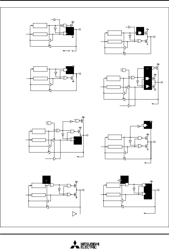
MITSUBISHI MICROCOMPUTERS
3886 Group
SINGLE-CHIP 8-BIT CMOS MICROCOMPUTER
(1) Port P00
P00–P03 output structure selection bit
|
Direction |
|
register |
Data bus |
Port latch |
Comparator reference power source input |
|
|
Comparator reference input |
|
pin select bit |
(3) Port P2 |
|
|
Direction |
|
register |
Data bus |
Port latch |
(2) Ports P01–P07,P1
P00–P03,
P04–P07,
P10–P13,
P14–P17 output structure selection bits
|
Direction |
|
register |
Data bus |
Port latch |
(4) Port P30 |
P30–P33 pull-up control bit |
||
PWM0 output pin selection bit |
|||
|
|||
|
PWM0 enable bit |
|
|
|
Direction |
|
|
|
register |
|
|
Data bus |
Port latch |
|
|
|
PWM00 output |
Comparator |
|
|
|
Key-on wake-up input |
|
(5) Port P31 |
P30–P33 pull-up control bit |
||
PWM1 output pin selection bit |
|||
|
|||
|
PWM1 enable bit |
|
|
|
Direction |
|
|
|
register |
|
|
Data bus |
Port latch |
|
|
PWM10 output |
|
Comparator |
|
|
Key-on wake-up input |
(6) Ports P32–P37 |
|
|
|
P30–P33, |
pull-up control bit |
|
P34–P37 |
|
|
Direction |
|
|
register |
|
Data bus |
Port latch |
|
Comparator Key-on wake-up input
(7) Port P40 |
|
Port XC switch bit |
|
|
Direction |
|
register |
Data bus |
Port latch |
(8) Port P41 |
|
Port XC switch bit |
|
|
Direction |
|
register |
Data bus |
Port latch |
Oscillator |
|
|||||
Port P41 |
|
|
|
|
Sub-clock generating circuit input |
|
|
|
|||||
|
|
|
|
|
|
|
|
|
|
|
|
|
|
Port XC switch bit |
|
|||||
Fig. 10 Port block diagram (1)
14
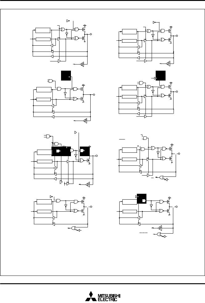
MITSUBISHI MICROCOMPUTERS
3886 Group
SINGLE-CHIP 8-BIT CMOS MICROCOMPUTER
(9) Port P42 |
|
|
|
(10) Port P43 |
|
|
P4 output structure selection bit |
|
|
|
P4 output structure selection bit |
|
|
|
|
|
|
|
||
|
|
|
|
|
|
|
|
|
|
|
|
|
|
OBF00 output enable bit
OBF01 output enable bit
Direction |
Direction |
|
register |
||
register |
||
|
Data bus |
Port latch |
Data bus |
Port latch |
|
|
|
|||
|
1 |
|
1 |
|
|
|
|
||
|
2 |
|
2 |
|
|
|
|
||
|
OBF00 output |
|
OBF01 output |
|
|
INT0 interrupt input |
|
INT1 interrupt input |
|
|
|
|
||
(11) Port P44 |
(12) Port P45 |
|||
|
P4 output structure selection bit |
P45/TXD P-channel output disable bit |
||
Serial I/O1 enable bit |
||||
Serial I/O1 enable bit |
||||
Receive enable bit |
||||
|
|
|
Transmit enable bit |
|
|
Direction |
Direction |
|
register |
|
|
register |
|
|
Data bus |
Port latch |
Data bus |
Port latch |
|
|
|
1 |
|
1 |
2 |
|
|
|
|
2 |
Serial I/O1 output |
|
|
|
|
Serial I/O1 input |
|
(13) Port P46
Serial I/O1 P4 output structure selection bit 
 synchronous clock selection bit
Serial I/O1 enable bit
Serial I/O1 mode selection bit
Serial I/O1 enable bit
OBF10 output enable bit
|
Direction |
|
register |
Data bus |
Port latch |
|
1 |
|
2 |
Serial I/O1 clock output 

OBF10 output 

Serial I/O1 external clock input
(14) Port P47
Serial I/O1 mode selection bit
Serial I/O1 enable bit 
SRDY1 output enable bit 
Data bus buffer function selection bit 

|
Direction |
|
register |
Data bus |
Port latch |
Serial I/O1 ready output |
3 |
S1 input |
Data bus buffer function |
|
selection bit |
(15) Port P50 |
|
|
|
(16) Ports P51,P52,P53 |
|
|
Data bus buffer enable bit |
|
|
|
Data bus buffer enable bit |
|
|
|
|
|
|
|||
Direction |
Direction |
register |
register |
Data bus |
Port latch |
Data bus |
Port latch |
|
A0 input |
3 |
INT20, INT30, INT40 interrupt input |
|
|
Data bus buffer |
3 |
|
enable bit |
||
S0,R,W input |
||
|
||
|
Data bus buffer |
|
|
enable bit |
1. The input level can be switched between CMOS compatible input level and TTL level by the P4 input level selection bit of the port control register 2 (address 002F16).
2. The input level can be switched between CMOS compatible input level and TTL level by the P4 input level selection bit of the port control register 2 (address 002F16).
The port P8 and port P4 input register can be switched by the P8 function selection bit of the port control register 2 (address 002F16).3. The input level can be switched between CMOS compatible input level and TTL level by the input level selection bit of the data bus buffer
control register (address 002A16).
Fig. 11 Port block diagram (2)
15
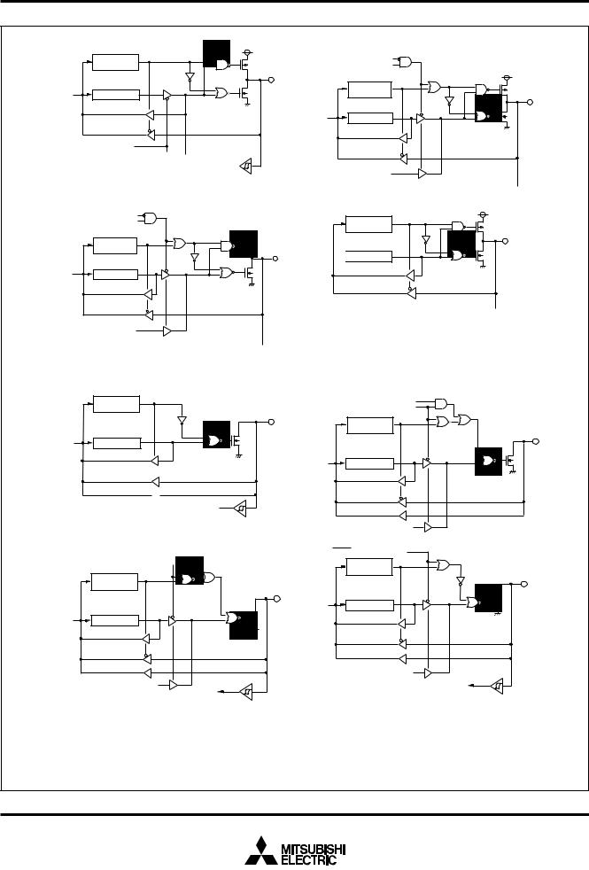
MITSUBISHI MICROCOMPUTERS
3886 Group
SINGLE-CHIP 8-BIT CMOS MICROCOMPUTER
(17) Ports P54,P55 |
|
|
Direction |
|
register |
Data bus |
Port latch |
Pulse output mode
Timer output 

CNTR0,CNTR1 interrupt input
(19) Port P57
PWM1 output pin selection bit
PWM1 enable bit
|
Direction |
|
register |
Data bus |
Port latch |
|
PWM11 output |
D-A converter output 

D-A2 output enable bit
(18) Port P56
PWM0 output pin selection bit
PWM0 enable bit
|
Direction |
|
register |
Data bus |
Port latch |
|
PWM01 output |
D-A converter output

D-A1 output enable bit
(20) Port P6
Direction register
Data bus 
 Port latch
A-D converter input 


Analog input pin selection bit
(21) Port P70
Direction register
Data bus |
Port latch |
4 
5 
Serial I/O2 input 
(23) Port P72
Serial I/O2 synchronization clock selection bit 
 Serial I/O2 port selection bit
|
Direction |
|
register |
Data bus |
Port latch |
|
4 |
|
5 |
|
Serial I/O2 clock output |
|
Serial I/O2 |
|
external clock input |
(22) Port P71 |
|
Serial IO/2 transmit completion signal |
|
Serial I/O2 port selection bit |
|
|
Direction |
|
register |
Data bus |
Port latch |
|
4 |
|
5 |
|
Serial I/O2 output |
(24) Port P73 |
|
|
SRDY2 output enable bit |
|
Direction |
|
register |
Data bus |
Port latch |
|
4 |
|
5 |
|
Serial I/O2 ready output |
|
INT21 interrupt input |
4. The input level can be switched between CMOS compatible input level and TTL level by the P7 input level selection bit of the port control register 2 (address 002F16).
5. The input level can be switched between CMOS compatible input level and TTL level by the P7 input level selection bit of the port control register 2 (address 002F16).
The port P8 direction register and port P7 input register can be switched by the P8 function selection bit of the port control register 2 (address 002F16).
Fig. 12 Port block diagram (3)
16

MITSUBISHI MICROCOMPUTERS
3886 Group
SINGLE-CHIP 8-BIT CMOS MICROCOMPUTER
(25) Ports P74,P75
Direction register
Data bus |
Port latch |
4 
5 
INT31,INT41 interrupt input 
(27) Port P77
I2C-BUS interface enable bit
|
Direction |
|
register |
Data bus |
Port latch |
|
SCL output |
|
6 |
|
SCL input |
(26) Port P76
I2C-BUS interface enable bit
|
Direction |
|
register |
Data bus |
Port latch |
|
SDA output |
|
6 |
|
SDA input |
(28) Port P8 |
S0 |
|
|
S1 |
R |
Data bus buffer enable bit |
|
|
|
Direction |
|
|
register |
|
Data bus |
Port latch |
|

 Output buffer 0

 Status register 0

Output buffer 1 


 Status register 1

3
Input buffer 0
3
Input buffer 1
6. The input level can be switched between CMOS compatible input level and SMBUS level by the I2C-BUS interface pin input selection bit of the I2C control register (address 001516).
Fig. 13 Port block diagram (4)
17
MITSUBISHI MICROCOMPUTERS
3886 Group
SINGLE-CHIP 8-BIT CMOS MICROCOMPUTER
b7 |
b0 |
Port control register 1 (PCTL1: address 002E16)
P00–P03 output structure selection bit
0:CMOS
1:N-channel open-drain
P04–P07 output structure selection bit
0:CMOS
1:N-channel open-drain
P10–P13 output structure selection bit
0:CMOS
1:N-channel open-drain
P14–P17 output structure selection bit
0:CMOS
1:N-channel open-drain P30–P33 pull-up control bit
0:No pull-up
1:Pull-up
P34–P37 pull-up control bit
0:No pull-up
1:Pull-up PWM0 enable bit
0:PWM0 output disabled
1:PWM0 output enabled PWM1 enable bit
0:PWM1 output disabled
1:PWM1 output enabled
b7 |
b0 |
Port control register 2 (PCTL2: address 002F16)
P4 input level selection bit (P42–P46)
0:CMOS level input
1:TTL level input
P7 input level selection bit (P70–P75)
0:CMOS level input
1:TTL level input
P4 output structure selection bit (P42, P43, P44, P46)
0:CMOS
1:N-channel open-drain P8 function selection bit
0:Port P8/Port P8 direction register
1:Port P4 input register/Port P7 input register INT2, INT3, INT4 interrupt switch bit
0:INT20, INT30, INT40 interrupt
1:INT21, INT31, INT41 interrupt Timer Y count source selection bit
0:f(XIN)/16 (f(XCIN)/16 in low-speed mode)
1:f(XCIN)
Oscillation stabilizing time set after STP instruction released bit
0:Automatic set “0116” to timer 1 and “FF16” to prescaler 12
1:No automatic set
Port output P42/P43 clear function selection bit
0:Only software clear
1:Software clear and output data bus buffer 0 reading (system bus side)
Fig. 14 Structure of port I/O related register
18

MITSUBISHI MICROCOMPUTERS
3886 Group
SINGLE-CHIP 8-BIT CMOS MICROCOMPUTER
INTERRUPTS
Interrupts occur by 16 sources among 21 sources: nine external, eleven internal, and one software.
Interrupt Control
Each interrupt is controlled by an interrupt request bit, an interrupt enable bit, and the interrupt disable flag except for the software interrupt set by the BRK instruction. An interrupt occurs if the corresponding interrupt request and enable bits are “1” and the interrupt disable flag is “0”.
Interrupt enable bits can be set or cleared by software.
Interrupt request bits can be cleared by software, but cannot be set by software.
The BRK instruction cannot be disabled with any flag or bit. The I
(interrupt disable) flag disables all interrupts except the BRK instruction interrupt.
When several interrupts occur at the same time, the interrupts are received according to priority.
Interrupt Source Selection
Any of the following interrupt sources can be selected by the interrupt source selection register (address 003916).
1.INT0 or Input buffer full
2.INT1 or Output buffer empty
3.Serial I/O1 transmission or SCLSDA
4.CNTR0 or SCLSDA
5.Serial I/O2 or I2C
6.INT2 or I2C
7.CNTR1 or Key-on wake-up
8.A-D conversion or Key-on wake-up
External Interrupt Pin Selection
The occurrence sources of the external interrupt INT2, INT3, and
INT4 can be selected from either input from INT20, INT30, INT40 pin, or input from INT21, INT31, INT41 pin by the INT2, INT3, INT4 interrupt switch bit (bit 4 of address 002F16).
Interrupt Operation
By acceptance of an interrupt, the following operations are automatically performed:
1.The contents of the program counter and the processor status register are automatically pushed onto the stack.
2.The interrupt disable flag is set and the corresponding interrupt request bit is cleared.
3.The interrupt jump destination address is read from the vector table into the program counter.
■ Notes
When setting of the following register or bit is changed, the interrupt request bit may be set to “1.”
•Interrupt edge selection register (address 003A16)
•Interrupt source selection register (address 003916)
•INT2, INT3, INT4 interrupt switch bit of Port control register 2 (bit
4 of address 002F16)
Accept the interrupt after clearing the interrupt request bit to “0” after interrupt is disabled and the above register or bit is set.
19

MITSUBISHI MICROCOMPUTERS
3886 Group
SINGLE-CHIP 8-BIT CMOS MICROCOMPUTER
Table 6 Interrupt vector addresses and priority
|
Interrupt Source |
|
Priority |
Vector Addresses (Note 1) |
|
|
|
|
|
|
|
Interrupt Request |
|
|
|
|
|
|
|
|
|
|
|
|
|
Remarks |
|||||||||||||||||||||||||||||||||||||||||||||||||||||||||
|
|
High |
Low |
|
|
|
|
Generating Conditions |
|
|
|
|
|
|
|
|
|
|
|
|
|
||||||||||||||||||||||||||||||||||||||||||||||||||||||||||||||
|
|
|
|
|
|
|
|
|
|
|
|
|
|
|
|
|
|
|
|
|
|
|
|
|
|
|
|
|
|
|
|
|
|
|
|
|
|
|
|
|
|
|
|
|
|
|
|
|
|
|
|
|
|
|
|
||||||||||||||||||||||||||||
|
|
|
|
|
|
|
|
|
|
|
|
|
|
|
|
|
|
|
|
|
|
|
|
|
|
|
|
|
|
|
|
|
|
|
|
|
|
|
|
|
|
|
|
|
|
|
|
|
|
|
|
|
|
|
|
|
|
|
|
|
|
|
|
|
|
|
|
|
|
|
|
|
|
|
|
|
|
|
|
|
|
|
|
|
Reset (Note 2) |
|
1 |
FFFD16 |
FFFC16 |
At reset |
|
|
Non-maskable |
||||||||||||||||||||||||||||||||||||||||||||||||||||||||||||||||||||||||||
|
|
|
|
|
|
|
|
|
|
|
|
|
|
|
|
|
|
|
|
|
|
|
|
|
|
|
|
|
|
|
|
|
|
|
|
|
|
|
|
|
|
|
|
|
|
|
|
|
|
|
|
|
|
|
|
|
|
|
|
|
|
|
|
|
|
|
|
|
|
|
|
|
|
|
|
|
|
|
|
|
|
|
|
|
INT0 |
|
|
|
|
At detection of either rising or |
|
|
External interrupt |
||||||||||||||||||||||||||||||||||||||||||||||||||||||||||||||||||||||||||
|
|
2 |
FFFB16 |
FFFA16 |
falling edge of INT0 input |
|
|
(active edge selectable) |
|||||||||||||||||||||||||||||||||||||||||||||||||||||||||||||||||||||||||||
|
|
|
|
|
|
|
|
|
|
|
|
|
|
|
|
|
|
|
|||||||||||||||||||||||||||||||||||||||||||||||||||||||||||||||||
|
|
|
|
|
|
|
|
|
|
|
|
|
|
|
|
|
|
|
|
|
|
|
|
|
|
|
|
|
|
|
|
|
|
|
|
|
|
|
|
|
|
|
|
|
|
|
|
|
|
|
|
|
|
|
|
|
|
|
|
|
|
|
|
|
|
|
|
|
|
|
|
|
|
|
|
|
|
|
|
|
|||
|
Input buffer full |
|
|
|
|
At input data bus buffer writing |
|
|
|
|
|
|
|
|
|
|
|
|
|
|
|
|
|
|
|
|
|
|
|
|
|
|
|
|
|
|
|
|
|
|
|||||||||||||||||||||||||||||||||||||||||||
|
(IBF) |
|
|
|
|
|
|
|
|
|
|
|
|
|
|
|
|
|
|
|
|
|
|
|
|
|
|
|
|
|
|
|
|
|
|
|
|
|
|
||||||||||||||||||||||||||||||||||||||||||||
|
|
|
|
|
|
|
|
|
|
|
|
|
|
|
|
|
|
|
|
|
|
|
|
|
|
|
|
|
|
|
|
|
|
|
|
|
|
|
|
|
|
|
|
|
|
|
|
|
|
|
|
|
|
|
|
|
|
|
|
|
|
|
|
|
|
|
|
|
|||||||||||||||
|
|
|
|
|
|
|
|
|
|
|
|
|
|
|
|
|
|
|
|
|
|
|
|
|
|
|
|
|
|
|
|
|
|
|
|
|
|
|
|
|
|
|
|
|
|
|
|
|
|
|
|
|
|
|
|
|
|
|
|
|
|
|
|
|
|
|
|
|
|
|
|
|
|
|
|
|
|
|
|
|
|
|
|
|
INT1 |
|
|
|
|
At detection of either rising or |
|
|
External interrupt |
||||||||||||||||||||||||||||||||||||||||||||||||||||||||||||||||||||||||||
|
|
|
|
|
falling edge of INT1 input |
|
|
(active edge selectable) |
|||||||||||||||||||||||||||||||||||||||||||||||||||||||||||||||||||||||||||
|
|
|
|
|
|
|
|
|
|
|
|
|
|
|
|
|
|
|
|
|
|
||||||||||||||||||||||||||||||||||||||||||||||||||||||||||||||
|
|
|
|
|
|
|
|
|
|
|
|
|
|
|
|
|
3 |
FFF916 |
FFF816 |
|
|
|
|
|
|
|
|
|
|
|
|
|
|
|
|
|
|
|
|
|
|
|
|
|
|
|
|
|
|
|
|
|
|
|
|
|
|
|
|
|
|
|
|
|
|
|
|
|
|
|
|
|
|
|
|
|
|
|
|
|
|
|
|
|
Output buffer |
|
At output data bus buffer read- |
|
|
|
|
|
|
|
|
|
|
|
|
|
|
|
|
|
|
|
|
|
|
|
|
|
|
|
|
|
|
|
|
|
|
||||||||||||||||||||||||||||||||||||||||||||||
|
|
|
|
|
|
|
|
|
|
|
|
|
|
|
|
|
|
|
|
|
|
|
|
|
|
|
|
|
|
|
|
|
|
|
|
|
|
|
|||||||||||||||||||||||||||||||||||||||||||||
|
empty (OBE) |
|
|
|
|
ing |
|
|
|
|
|
|
|
|
|
|
|
|
|
|
|
|
|
|
|
|
|
|
|
|
|
|
|
|
|
|
|
|
|
|
|||||||||||||||||||||||||||||||||||||||||||
|
|
|
|
|
|
|
|
|
|
|
|
|
|
|
|
|
|
|
|
|
|
|
|
|
|
|
|
|
|
|
|
|
|
|
|
|
|
|
|
|
|
|
|
|
|
|
|
|
|
|
|
|
|
|
|
|
|
|
|
|
|
|
|
|
|
|
|
|
|
|
|
|
|
|
|
|
|
|
|
|
|
|
|
|
Serial I/O1 |
|
4 |
FFF716 |
FFF616 |
At completion of serial I/O1 data |
|
|
Valid when serial I/O1 is selected |
||||||||||||||||||||||||||||||||||||||||||||||||||||||||||||||||||||||||||
|
reception |
|
reception |
|
|
||||||||||||||||||||||||||||||||||||||||||||||||||||||||||||||||||||||||||||||
|
|
|
|
|
|
|
|
|
|
|
|
|
|
|
|
|
|
|
|
|
|
|
|
|
|
|
|
|
|
|
|
|
|
|
|
|
|
|
|||||||||||||||||||||||||||||||||||||||||||||
|
|
|
|
|
|
|
|
|
|
|
|
|
|
|
|
|
|
|
|
|
|
|
|
|
|
|
|
|
|
|
|
|
|
|
|
|
|
|
|
|
|
|
|
|
|
|
|
|
|
|
|
|
|
|
|
|
|
|
|
|
|
|
|
|
|
|
|
|
|
|
|
|
|
|
|
|
|
|
|
|
|
|
|
|
Serial I/O1 |
|
|
|
|
At completion of serial I/O1 |
|
|
|
|
|
|
|
|
|
|
|
|
|
|
|
|
|
|
|
|
|
|
|
|
|
|
|
|
|
|
|
|
|
|
|||||||||||||||||||||||||||||||||||||||||||
|
|
|
|
|
transfer shift or when transmis- |
|
|
Valid when serial I/O1 is selected |
|||||||||||||||||||||||||||||||||||||||||||||||||||||||||||||||||||||||||||
|
transmission |
|
|
|
|
|
|
||||||||||||||||||||||||||||||||||||||||||||||||||||||||||||||||||||||||||||
|
|
5 |
FFF516 |
FFF416 |
sion buffer is empty |
|
|
|
|
|
|
|
|
|
|
|
|
|
|
|
|
|
|
|
|
|
|
|
|
|
|
|
|
|
|
|
|
|
|
||||||||||||||||||||||||||||||||||||||||||||
|
|
|
|
|
|
|
|
|
|
|
|
|
|
|
|
|
|
|
|
|
|
|
|
|
|
|
|
|
|
|
|
|
|
|
|
|
|
|
|
|
|
|
|
|
|
|
|
|
|
|
|||||||||||||||||||||||||||||||||
|
|
|
|
|
|
|
|
|
|
|
|
|
|
|
|
|
|
|
|
|
|
|
|
|
|
|
|
|
|
|
|
|
|
|
|
|
|
|
|
|
|
|
|
|
|
|
|
|
|
|
|
|
|
|
|
|
|
|
|
|
|
|
|
|
|
|
|
|
|
|
|
|
|
|
|
|
|
|
|
|
|
|
|
|
SCL, SDA |
|
|
|
|
At detection of either rising or |
|
|
External interrupt |
||||||||||||||||||||||||||||||||||||||||||||||||||||||||||||||||||||||||||
|
|
|
|
|
falling edge of SCL or SDA |
|
|
(active edge selectable) |
|||||||||||||||||||||||||||||||||||||||||||||||||||||||||||||||||||||||||||
|
|
|
|
|
|
|
|
|
|
|
|
|
|
|
|
|
|
|
|
|
|
||||||||||||||||||||||||||||||||||||||||||||||||||||||||||||||
|
Timer X |
|
6 |
FFF316 |
FFF216 |
At timer X underflow |
|
|
|
|
|
|
|
|
|
|
|
|
|
|
|
|
|
|
|
|
|
|
|
|
|
|
|
|
|
|
|
|
|
|
|||||||||||||||||||||||||||||||||||||||||||
|
|
|
|
|
|
|
|
|
|
|
|
|
|
|
|
|
|
|
|
|
|
|
|
|
|
|
|
|
|
|
|
|
|
|
|
|
|
|
|
|
|
|
|
|
|
|
|
|
|
|
|
|
|
|
|||||||||||||||||||||||||||||
|
Timer Y |
|
7 |
FFF116 |
FFF016 |
At timer Y underflow |
|
|
|
|
|
|
|
|
|
|
|
|
|
|
|
|
|
|
|
|
|
|
|
|
|
|
|
|
|
|
|
|
|
|
|||||||||||||||||||||||||||||||||||||||||||
|
|
|
|
|
|
|
|
|
|
|
|
|
|
|
|
|
|
|
|
|
|
|
|
|
|
|
|
|
|
|
|
|
|
|
|
|
|
|
|
|
|
|
|
|
|
|
|
|
|
|
|
|
|
|
|||||||||||||||||||||||||||||
|
Timer 1 |
|
8 |
FFEF16 |
FFEE16 |
At timer 1 underflow |
|
|
STP release timer underflow |
||||||||||||||||||||||||||||||||||||||||||||||||||||||||||||||||||||||||||
|
|
|
|
|
|
|
|
|
|
|
|
|
|
|
|
|
|
|
|
|
|
|
|
|
|
|
|
|
|
|
|
|
|
|
|
|
|
|
|
|
|
|
|
|
|
|
|
|
|
|
|
|
|
|
|||||||||||||||||||||||||||||
|
Timer 2 |
|
9 |
FFED16 |
FFEC16 |
At timer 2 underflow |
|
|
|
|
|
|
|
|
|
|
|
|
|
|
|
|
|
|
|
|
|
|
|
|
|
|
|
|
|
|
|
|
|
|
|||||||||||||||||||||||||||||||||||||||||||
|
CNTR0 |
|
|
|
|
At detection of either rising or |
|
|
External interrupt |
||||||||||||||||||||||||||||||||||||||||||||||||||||||||||||||||||||||||||
|
|
|
|
|
falling edge of CNTR0 input |
|
|
(active edge selectable) |
|||||||||||||||||||||||||||||||||||||||||||||||||||||||||||||||||||||||||||
|
|
|
|
|
|
|
|
|
|
|
|
|
|
|
|
|
10 |
FFEB16 |
FFEA16 |
|
|
||||||||||||||||||||||||||||||||||||||||||||||||||||||||||||||
|
|
|
|
|
|
|
|
|
|
|
|
|
|
|
|
|
|
|
|
|
|
|
|
|
|
|
|
|
|
|
|
|
|
|
|
|
|
|
|
|
|
|
|
|
|
|
|
|
|
|
|
|
|
|
|
|
|
|
|
|
|
|
|
|
|
|
|
|
|
|
|
|
|
|
|
|
|
|
|
|
|||
|
SCL, SDA |
|
At detection of either rising or |
|
|
External interrupt |
|||||||||||||||||||||||||||||||||||||||||||||||||||||||||||||||||||||||||||||
|
|
|
|
|
|
|
|||||||||||||||||||||||||||||||||||||||||||||||||||||||||||||||||||||||||||||
|
|
|
|
|
falling edge of SCL or SDA |
|
|
(active edge selectable) |
|||||||||||||||||||||||||||||||||||||||||||||||||||||||||||||||||||||||||||
|
|
|
|
|
|
|
|
|
|
|
|
|
|
|
|
|
|
|
|
|
|
||||||||||||||||||||||||||||||||||||||||||||||||||||||||||||||
|
|
|
|
|
|
|
|
|
|
|
|
|
|
|
|
|
|
|
|
|
|
|
|
|
|
|
|
|
|
|
|
|
|
|
|
|
|
|
|
|
|
|
|
|
|
|
|
|
|
|
|
|
|
|
|||||||||||||||||||||||||||||
|
CNTR1 |
|
|
|
|
At detection of either rising or |
|
|
External interrupt |
||||||||||||||||||||||||||||||||||||||||||||||||||||||||||||||||||||||||||
|
|
|
|
|
falling edge of CNTR1 input |
|
|
(active edge selectable) |
|||||||||||||||||||||||||||||||||||||||||||||||||||||||||||||||||||||||||||
|
|
|
|
|
|
|
|
|
|
|
|
|
|
|
|
|
11 |
FFE916 |
FFE816 |
|
|
||||||||||||||||||||||||||||||||||||||||||||||||||||||||||||||
|
|
|
|
|
|
|
|
|
|
|
|
|
|
|
|
|
|
|
|
|
|
|
|
|
|
|
|
|
|
|
|
|
|
|
|
|
|
|
|
|
|
|
|
|
|
|
|
|
|
|
|
|
|
|
|
|
|
|
|
|
|
|
|
|
|
|
|
|
|
|
|
|
|
|
|
|
|
|
|
|
|||
|
Key-on wake-up |
|
At falling of port P3 (at input) in- |
|
|
External interrupt (falling valid) |
|||||||||||||||||||||||||||||||||||||||||||||||||||||||||||||||||||||||||||||
|
|
|
|
|
|
|
|||||||||||||||||||||||||||||||||||||||||||||||||||||||||||||||||||||||||||||
|
|
|
|
|
put logical level AND |
|
|
||||||||||||||||||||||||||||||||||||||||||||||||||||||||||||||||||||||||||||
|
|
|
|
|
|
|
|
|
|
|
|
|
|
|
|
|
|
|
|
|
|
|
|
|
|
|
|
|
|
|
|
|
|
|
|
|
|
|
|
|
|
|
|
|
|
|
|
|
|
|
|
|
|
||||||||||||||||||||||||||||||
|
Serial I/O2 |
|
|
|
|
At completion of serial I/O2 data |
|
|
Valid when serial I/O2 is selected |
||||||||||||||||||||||||||||||||||||||||||||||||||||||||||||||||||||||||||
|
|
12 |
FFE716 |
FFE616 |
transfer |
|
|
||||||||||||||||||||||||||||||||||||||||||||||||||||||||||||||||||||||||||||
|
|
|
|
|
|
|
|
|
|
|
|
|
|
|
|
|
|
|
|
|
|
|
|
|
|
|
|
|
|
|
|
|
|
|
|
|
|
|
|
|
|
|
|
|
|
|
|
|
|
|
|||||||||||||||||||||||||||||||||
|
|
|
|
|
|
|
|
|
|
|
|
|
|
|
|
|
|
|
|
|
|
|
|
|
|
|
|
|
|
|
|
|
|
|
|
|
|
|
|
|
|
|
|
|
|
|
|
|
|
|
|
|
|
|
|
|
|
|
|
|
|
|
|
|
|
|
|
|
|
|
|
|
|
|
|
|
|
|
|
|
|
|
|
|
I2C |
|
|
|
|
At completion of data transfer |
|
|
|
|
|
|
|
|
|
|
|
|
|
|
|
|
|
|
|
|
|
|
|
|
|
|
|
|
|
|
|
|
|
|
|||||||||||||||||||||||||||||||||||||||||||
|
INT2 |
|
|
|
|
At detection of either rising or |
|
|
External interrupt |
||||||||||||||||||||||||||||||||||||||||||||||||||||||||||||||||||||||||||
|
|
13 |
FFE516 |
FFE416 |
falling edge of INT2 input |
|
|
(active edge selectable) |
|||||||||||||||||||||||||||||||||||||||||||||||||||||||||||||||||||||||||||
|
|
|
|
|
|
|
|
|
|
|
|
|
|
|
|
|
|
|
|||||||||||||||||||||||||||||||||||||||||||||||||||||||||||||||||
|
|
|
|
|
|
|
|
|
|
|
|
|
|
|
|
|
|
|
|
|
|
|
|
|
|
|
|
|
|
|
|
|
|
|
|
|
|
|
|
|
|
|
|
|
|
|
|
|
|
|
|
|
|
|
|||||||||||||||||||||||||||||
|
I2C |
|
|
|
|
At completion of data transfer |
|
|
|
|
|
|
|
|
|
|
|
|
|
|
|
|
|
|
|
|
|
|
|
|
|
|
|
|
|
|
|
|
|
|
|||||||||||||||||||||||||||||||||||||||||||
|
INT3 |
|
14 |
FFE316 |
FFE216 |
At detection of either rising or |
|
|
External interrupt |
||||||||||||||||||||||||||||||||||||||||||||||||||||||||||||||||||||||||||
|
|
falling edge of INT3 input |
|
|
(active edge selectable) |
||||||||||||||||||||||||||||||||||||||||||||||||||||||||||||||||||||||||||||||
|
|
|
|
|
|
|
|
|
|
|
|
|
|
|
|
|
|
|
|
|
|
||||||||||||||||||||||||||||||||||||||||||||||||||||||||||||||
|
|
|
|
|
|
|
|
|
|
|
|
|
|
|
|
|
|
|
|
|
|
|
|
||||||||||||||||||||||||||||||||||||||||||||||||||||||||||||
|
INT4 |
|
15 |
FFE116 |
FFE016 |
At detection of either rising or |
|
|
External interrupt |
||||||||||||||||||||||||||||||||||||||||||||||||||||||||||||||||||||||||||
|
|
falling edge of INT4 input |
|
|
(active edge selectable) |
||||||||||||||||||||||||||||||||||||||||||||||||||||||||||||||||||||||||||||||
|
|
|
|
|
|
|
|
|
|
|
|
|
|
|
|
|
|
|
|
|
|
||||||||||||||||||||||||||||||||||||||||||||||||||||||||||||||
|
|
|
|
|
|
|
|
|
|
|
|
|
|
|
|
|
|
|
|
|
|
|
|
|
|
|
|
|
|
|
|
|
|
|
|
|
|
|
|
|
|
|
|
|
|
|
|
|
|
|
|
|
|
|
|||||||||||||||||||||||||||||
|
A-D converter |
|
|
|
|
At completion of A-D conversion |
|
|
|
|
|
|
|
|
|
|
|
|
|
|
|
|
|
|
|
|
|
|
|
|
|
|
|
|
|
|
|
|
|
|
|||||||||||||||||||||||||||||||||||||||||||
|
|
|
|
|
|
|
|
|
|
|
|
|
|
|
|
|
16 |
FFDF16 |
FFDE16 |
|
|
|
|
|
|
|
|
|
|
|
|
|
|
|
|
|
|
|
|
|
|
|
|
|
|
|
|
|
|
|
|
|
|
|
|
|
|
|
|
|
|
|
|
|
|
|
|
|
|
|
|
|
|
|
|
|
|
|
|
|
|
|
|
|
Key-on wake-up |
|
At falling of port P3 (at input) in- |
|
|
External interrupt (falling valid) |
|||||||||||||||||||||||||||||||||||||||||||||||||||||||||||||||||||||||||||||
|
|
|
|
|
|
|
|||||||||||||||||||||||||||||||||||||||||||||||||||||||||||||||||||||||||||||
|
|
|
|
|
put logical level AND |
|
|
||||||||||||||||||||||||||||||||||||||||||||||||||||||||||||||||||||||||||||
|
|
|
|
|
|
|
|
|
|
|
|
|
|
|
|
|
|
|
|
|
|
|
|
|
|
|
|
|
|
|
|
|
|
|
|
|
|
|
|
|
|
|
|
|
|
|
|
|
|
|
|
|
|
||||||||||||||||||||||||||||||
|
|
|
|
|
|
|
|
|
|
|
|
|
|
|
|
|
|
|
|
|
|
|
|
||||||||||||||||||||||||||||||||||||||||||||||||||||||||||||
|
BRK instruction |
|
17 |
FFDD16 |
FFDC16 |
At BRK instruction execution |
|
|
Non-maskable software interrupt |
||||||||||||||||||||||||||||||||||||||||||||||||||||||||||||||||||||||||||
Notes 1: Vector addresses contain interrupt jump destination addresses.
2: Reset function in the same way as an interrupt with the highest priority.
20
MITSUBISHI MICROCOMPUTERS
3886 Group
SINGLE-CHIP 8-BIT CMOS MICROCOMPUTER
Interrupt request bit
Interrupt enable bit
Interrupt disable flag (I)
BRK instruction |
Interrupt request |
Reset |
|
Fig. 15 Interrupt control
b7
b7
b7
b0 Interrupt edge selection register  (INTEDGE : address 003A16)
INT0 active edge selection bit INT1 active edge selection bit Not used (returns “0” when read) INT2 active edge selection bit INT3 active edge selection bit
INT4 active edge selection bit
Not used (returns “0” when read) 0 : Falling edge active 1 : Rising edge active
|
|
|
|
|
|
|
b0 |
|
Interrupt request register 1 |
|
|
b7 |
|
|
|
|
|
|
|
b0 |
|
Interrupt request register 2 |
|
|||||||||||||
|
|
|
|
|
|
|
|
|
|
(IREQ1 : address 003C16) |
|
|
|
|
|
|
|
|
|
|
|
|
|
|
|
|
|
|
(IREQ2 : address 003D16) |
|||||||
|
|
|
|
|
|
|
|
|
|
|
|
|
|
|
|
|
|
|
|
|
|
|
|
|
|
|
|
|
|
|
|
|
|
|
||
|
|
|
|
|
|
|
|
|
|
|
|
INT0/input buffer full interrupt request |
|
|
|
|
|
|
|
|
|
|
|
|
|
|||||||||||
|
|
|
|
|
|
|
|
|
|
|
|
|
|
|
|
|
|
|
|
|
|
|
|
|
|
|
|
|
|
|
|
CNTR0/SCL, SDA interrupt request bit |
||||
|
|
|
|
|
|
|
|
|
|
|
|
|
|
|
|
|
|
|
|
|
|
|
|
|
|
|
|
|
|
|
|
|||||
|
|
|
|
|
|
|
|
|
|
|
|
bit |
|
|
|
|
|
|
|
|
|
|
|
|
|
|
|
|
|
|
|
|
CNTR1/key-on wake-up interrupt |
|||
|
|
|
|
|
|
|
|
|
|
|
|
|
|
|
|
|
|
|
|
|
|
|
|
|
|
|
|
|
|
|
|
|||||
|
|
|
|
|
|
|
|
|
|
|
|
INT1/output buffer empty interrupt |
|
|
|
|
|
|
|
|
|
|
|
|
|
|
|
|
|
|
|
|
request bit |
|||
|
|
|
|
|
|
|
|
|
|
|
|
|
|
|
|
|
|
|
|
|
|
|
|
|
|
|
|
|
|
|
|
|||||
|
|
|
|
|
|
|
|
|
|
|
|
request bit |
|
|
|
|
|
|
|
|
|
|
|
|
|
|
|
|
|
|
|
|
Serial I/O2/I2C interrupt request bit |
|||
|
|
|
|
|
|
|
|
|
|
|
|
|
|
|
|
|
|
|
|
|
|
|
|
|
|
|
|
|
|
|
|
|||||
|
|
|
|
|
|
|
|
|
|
|
|
Serial I/O1 receive interrupt request bit |
|
|
|
|
|
|
|
|
|
|
|
|
|
|
|
|
|
|
|
|
INT2/I2C interrupt request bit |
|||
|
|
|
|
|
|
|
|
|
|
|
|
|
|
|
|
|
|
|
|
|
|
|
|
|
|
|
|
|
|
|
|
|||||
|
|
|
|
|
|
|
|
|
|
|
|
Serial I/O1 transmit/SCL, SDA interrupt |
|
|
|
|
|
|
|
|
|
|
|
|
|
|
|
|
|
|
|
|
||||
|
|
|
|
|
|
|
|
|
|
|
|
|
|
|
|
|
|
|
|
|
|
|
|
|
|
|
|
|
|
|
|
INT3 interrupt request bit |
||||
|
|
|
|
|
|
|
|
|
|
|
|
request bit |
|
|
|
|
|
|
|
|
|
|
|
|
|
|
|
|
|
|
|
|
||||
|
|
|
|
|
|
|
|
|
|
|
|
|
|
|
|
|
|
|
|
|
|
|
|
|
|
|
|
|
|
|
|
INT4 interrupt request bit |
||||
|
|
|
|
|
|
|
|
|
|
|
|
Timer X interrupt request bit |
|
|
|
|
|
|
|
|
|
|
|
|
|
|
|
|
|
|
|
|
||||
|
|
|
|
|
|
|
|
|
|
|
|
|
|
|
|
|
|
|
|
|
|
|
|
|
|
|
|
|
|
|
|
AD converter/key-on wake-up interrupt |
||||
|
|
|
|
|
|
|
|
|
|
|
|
Timer Y interrupt request bit |
|
|
|
|
|
|
|
|
|
|
|
|
|
|
|
|
|
|
|
|
||||
|
|
|
|
|
|
|
|
|
|
|
|
|
|
|
|
|
|
|
|
|
|
|
|
|
|
|
|
|
|
|
|
request bit |
||||
|
|
|
|
|
|
|
|
|
|
|
|
Timer 1 interrupt request bit |
|
|
|
|
|
|
|
|
|
|
|
|
|
|
|
|
|
|
|
|
||||
|
|
|
|
|
|
|
|
|
|
|
|
|
|
|
|
|
|
|
|
|
|
|
|
|
|
|
|
|
|
|
|
Not used (returns “0” when read) |
||||
|
|
|
|
|
|
|
|
|
|
|
|
Timer 2 interrupt request bit |
|
|
|
|
|
|
|
|
|
|
|
|
|
|
|
|
|
|
|
|
||||
|
|
|
|
|
|
|
|
|
|
|
|
|
|
|
|
|
|
|
|
|
|
|
|
|
|
|
|
|
|
|
|
|
|
|
||
|
|
|
|
|
|
|
|
|
|
|
|
|
|
|
|
|
|
|
|
|
|
|
|
|
0 : No interrupt request issued |
|
|
|||||||||
|
|
|
|
|
|
|
|
|
|
|
|
|
|
|
|
|
|
|
|
|
|
|
|
|
|
|
|
|
||||||||
|
|
|
|
|
|
|
|
|
|
|
|
|
|
|
|
|
|
|
|
|
|
|
|
|
|
|
1 : Interrupt request issued |
|
|
|||||||
|
|
|
|
|
|
|
b0 |
|
|
|
|
b7 |
|
||||
|
|
|
|
|
|
|
|
|
|
Interrupt control register 1 |
|
|
|
|
|
|
|
|
|
|
|
|
|
|
|
|
|
|
|
|
|
|
|
||
|
|
|
|
|
|
|
|
|
|
(ICON1 : address 003E16) |
|
|
|
|
|
|
|
|
|
|
|
|
|
|
|
|
|
|
|
|
|
|
|
||
|
|
|
|
|
|
|
|
|
|
|
|
|
|
|
|
|
|
|
|
|
|
|
|
|
|
|
|
INT0/input buffer full interrupt enable bit |
|
||||||
|
|
|
|
|
|
|
|
|
|
|
|
|
|
|
|
||
|
|
|
|
|
|
|
|
|
|
|
INT1/output buffer empty interrupt |
|
|
|
|
|
|
|
|
|
|
|
|
|
|
|
|
|
|
|
|
|
|
||
|
|
|
|
|
|
|
|
|
|
|
enable bit |
|
|
|
|
|
|
|
|
|
|
|
|
|
|
|
|
|
Serial I/O1 receive interrupt enable bit |
|
|
|
|
|
|
|
|
|
|
|
|
|
|
|
|
|
|
|
|
|
|
||
|
|
|
|
|
|
|
|
|
|
|
Serial I/O1 transmit/SCL, SDA interrupt |
|
|
|
|
|
|
|
|
|
|
|
|
|
|
|
|
|
|
|
|
|
|
||
|
|
|
|
|
|
|
|
|
|
|
enable bit |
|
|
|
|
|
|
|
|
|
|
|
|
|
|
|
|
|
Timer X interrupt enable bit |
|
|
|
|
|
|
|
|
|
|
|
|
|
|
|
|
|
|
|
|
|
|
||
|
|
|
|
|
|
|
|
|
|
|
Timer Y interrupt enable bit |
|
|
|
|
|
|
|
|
|
|
|
|
|
|
|
|
|
|
|
|
|
|
||
|
|
|
|
|
|
|
|
|
|
|
Timer 1 interrupt enable bit |
|
|
|
|
|
|
|
|
|
|
|
|
|
|
|
|
|
|
|
|
|
|
||
|
|
|
|
|
|
|
|
|
|
|
Timer 2 interrupt enable bit |
|
|
|
|
|
|
|
|
|
|
|
|
|
|
|
|
|
|
|
|
|
|
|
|
b0 Interrupt control register 2 (ICON2 : address 003F16)
CNTR0/SCL, SDA interrupt enable bit CNTR1/key-on wake-up interrupt enable bit
Serial I/O2/I2C interrupt enable bit
INT2/I2C interrupt enable bit INT3 interrupt enable bit INT4 interrupt enable bit
AD converter/key-on wake-up interrupt enable bit
Not used (returns “0” when read) (Do not write “1” to this bit)
0 : Interrupts disabled
1 : Interrupts enabled
Fig. 16 Structure of interrupt-related registers (1)
21
MITSUBISHI MICROCOMPUTERS
3886 Group
SINGLE-CHIP 8-BIT CMOS MICROCOMPUTER
|
b7 |
|
|
|
|
|
b0 |
|
|
|
|
||
|
|
|
|
|
|
|
|
|
|
|
Interrupt source selection register |
||
|
|
|
|
|
|
|
|
|
|
|
|
(INTSEL: address 003916) |
|
|
|
|
|
|
|
|
|
|
|
|
|
INT0/input buffer full interrupt source selection bit |
|
|
|
|
|
|
|
|
|
|
|
|
|
||
|
|
|
0 |
: INT0 interrupt |
|||||||||
|
|
|
1 |
: Input buffer full interrupt |
|||||||||
INT1/output buffer empty interrupt source selection bit 0 : INT1 interrupt
1 : Output buffer empty interrupt
Serial I/O1 transmit/SCL,SDA interrupt source selection bit 0 : Serial I/O1 transmit interrupt
1 : SCL,SDA interrupt
(Do not write “1” to these bits simultaneously.)
CNTR0/SCL,SDA interrupt source selection bit 0 : CNTR0 interrupt
1 : SCL,SDA interrupt
Serial I/O2/I2C interrupt source selection bit 0 : Serial I/O2 interrupt
1 : I2C interrupt
(Do not write “1” to these bits simultaneously.)
INT2/I2C interrupt source selection bit 0 : INT2 interrupt
1 : I2C interrupt
CNTR1/key-on wake-up interrupt source selection bit 0 : CNTR1 interrupt
1 : Key-on wake-up interrupt
(Do not write “1” to these bits simultaneously.)
AD converter/key-on wake-up interrupt source selection bit 0 : A-D converter interrupt
1 : Key-on wake-up interrupt
Fig. 17 Structure of interrupt-related registers (2)
22
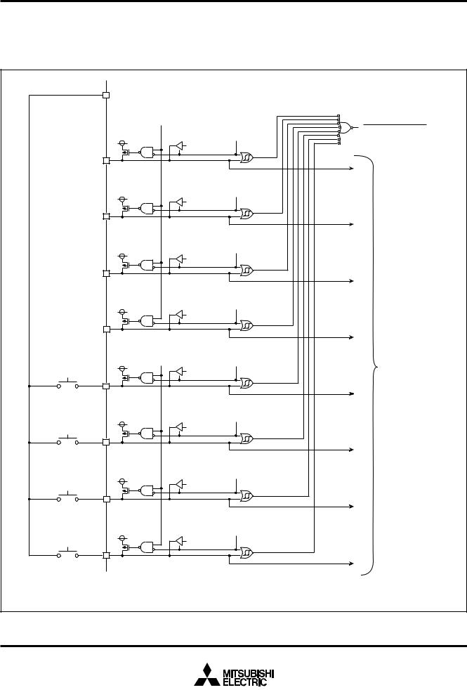
MITSUBISHI MICROCOMPUTERS
3886 Group
SINGLE-CHIP 8-BIT CMOS MICROCOMPUTER
Key Input Interrupt (Key-on Wake Up)
A Key input interrupt request is generated by applying “L” level to any pin of port P3 that have been set to input mode. In other words, it is generated when AND of input level goes from “1” to
“0”. An example of using a key input interrupt is shown in Figure 18, where an interrupt request is generated by pressing one of the keys consisted as an active-low key matrix which inputs to ports
P30–P33.
Port PXx |
|
|
|
|
“L” level output |
|
|
|
|
|
Port control register 1 |
|
|
|
|
Bit 5 = “1” |
|
|
|
|
|
|
Port P37 |
Key input interrupt request |
|
|
direction register = “1” |
|
|
|
Port P37 |
|
|
|
|
|
latch |
|
|
P37 output |
|
|
|
|
|
|
|
Port P36 |
|
|
|
|
direction register = “1” |
|
|
Port P36 |
|
|
|
|
|
latch |
|
|
P36 output |
|
|
|
|
|
|
|
Port P35 |
|
|
|
|
direction register = “1” |
|
|
Port P35 |
|
|
|
|
|
latch |
|
|
P35 output |
|
|
|
|
|
|
|
Port P34 |
|
|
|
|
direction register = “1” |
|
|
Port P34 |
|
|
|
|
|
latch |
|
|
P34 output |
|
|
|
|
|
Port control register 1 |
Port P33 |
|
|
|
Bit 4 = “1” |
|
direction register = “0” |
Port P3 |
|
Port P33 |
|
||
|
Input reading circuit |
|||
P33 input |
|
latch |
|
|
|
|
Comparator circuit |
||
|
|
|
Port P32 |
|
|
|
|
direction register = “0” |
|
|
Port P32 |
|
|
|
P32 input |
|
latch |
|
|
|
|
|
|
|
|
|
|
Port P31 |
|
|
|
|
direction register = “0” |
|
|
Port P31 |
|
|
|
P31 input |
|
latch |
|
|
|
|
|
|
|
|
|
|
Port P30 |
|
|
|
|
direction register = “0” |
|
|
Port P30 |
|
|
|
P30 input |
|
latch |
|
|
|
|
|
|
|
P-channel transistor for pull-upCMOS output buffer
Fig. 18 Connection example when using key input interrupt and port P3 block diagram
23

MITSUBISHI MICROCOMPUTERS
3886 Group
SINGLE-CHIP 8-BIT CMOS MICROCOMPUTER
TIMERS
The 3886 group has four timers: timer X, timer Y, timer 1, and timer 2.
The division ratio of each timer or prescaler is given by 1/(n + 1), where n is the value in the corresponding timer or prescaler latch. All timers are count down. When the timer reaches “0016”, an underflow occurs at the next count pulse and the corresponding timer latch is reloaded into the timer and the count is continued. When a timer underflows, the interrupt request bit corresponding to that timer is set to “1”.
b7 |
|
|
b0 |
|||||||||||||||
|
|
|
|
|
|
|
|
|
|
|
|
|
|
|
|
|
|
Timer XY mode register |
|
|
|
|
|
|
|
|
|
|
|
|
|
|
|
|
|
|
(TM : address 002316) |
|
|
|
|
|
|
|
|
|
|
|
|
|
|
|
|
|
|
Timer X operating mode bit |
|
|
|
|
|
|
|
|
|
|
|
|
|
|
|
|
|
|
|
|
|
|
|
|
|
|
|
|
|
|
|
|
|
|
|
|
|
|
|
|
|
|
|
|
|
|
|
|
|
|
|
|
|
|
|
|
b1b0 |
|
|
|
|
|
|
|
|
|
|
|
|
|
|
|
|
|
|
0 0: Timer mode |
|
|
|
|
|
|
|
|
|
|
|
|
|
|
|
|
|
|
0 1: Pulse output mode |
|
|
|
|
|
|
|
|
|
|
|
|
|
|
|
|
|
|
1 0: Event counter mode |
|
|
|
|
|
|
|
|
|
|
|
|
|
|
|
|
|
|
1 1: Pulse width measurement mode |
|
|
|
|
|
|
|
|
|
|
|
|
|
|
|
|
|
|
CNTR0 active edge selection bit |
|
|
|
|
|
|
|
|
|
|
|
|
|
|
|
|
|
|
0: Interrupt at falling edge |
|
|
|
|
|
|
|
|
|
|
|
|
|
|
|
|
|
|
Count at rising edge in event |
|
|
|
|
|
|
|
|
|
|
|
|
|
|
|
|
|
|
counter mode |
|
|
|
|
|
|
|
|
|
|
|
|
|
|
|
|
|
|
1: Interrupt at rising edge |
|
|
|
|
|
|
|
|
|
|
|
|
|
|
|
|
|
|
Count at falling edge in event |
|
|
|
|
|
|
|
|
|
|
|
|
|
|
|
|
|
|
counter mode |
|
|
|
|
|
|
|
|
|
|
|
|
|
|
|
|
|
|
Timer X count stop bit |
|
|
|
|
|
|
|
|
|
|
|
|
|
|
|
|
|
|
|
|
|
|
|
|
|
|
|
|
|
|
|
|
|
|
|
|
|
0: Count start |
|
|
|
|
|
|
|
|
|
|
|
|
|
|
|
|
|
|
1: Count stop |
|
|
|
|
|
|
|
|
|
|
|
|
|
|
|
|
|
|
Timer Y operating mode bit |
|
|
|
|
|
|
|
|
|
|
|
|
|
|
|
|
|
||
|
|
|
|
|
|
|
|
|
|
|
|
|
|
|
|
|
|
b5b4 |
|
|
|
|
|
|
|
|
|
|
|
|
|
|
|
|
|
|
0 0: Timer mode |
|
|
|
|
|
|
|
|
|
|
|
|
|
|
|
|
|
|
0 1: Pulse output mode |
|
|
|
|
|
|
|
|
|
|
|
|
|
|
|
|
|
|
1 0: Event counter mode |
|
|
|
|
|
|
|
|
|
|
|
|
|
|
|
|
|
|
1 1: Pulse width measurement mode |
|
|
|
|
|
|
|
|
|
|
|
|
|
|
|
|
|
|
CNTR1 active edge selection bit |
|
|
|
|
|
|
|
|
|
|
|
|
|
|
|
|
|
|
0: Interrupt at falling edge |
|
|
|
|
|
|
|
|
|
|
|
|
|
|
|
|
|
|
Count at rising edge in event |
|
|
|
|
|
|
|
|
|
|
|
|
|
|
|
|
|
|
counter mode |
|
|
|
|
|
|
|
|
|
|
|
|
|
|
|
|
|
|
1: Interrupt at rising edge |
|
|
|
|
|
|
|
|
|
|
|
|
|
|
|
|
|
|
Count at falling edge in event |
|
|
|
|
|
|
|
|
|
|
|
|
|
|
|
|
|
|
counter mode |
|
|
|
|
|
|
|
|
|
|
|
|
|
|
|
|
|
|
Timer Y count stop bit |
|
|
|
|
|
|
|
|
|
|
|
|
|
|
|
|
|
|
0: Count start |
|
|
|
|
|
|
|
|
|
|
|
|
|
|
|
|
|
|
1: Count stop |
Fig. 19 Structure of timer XY mode register
Timer 1 and Timer 2
The count source of prescaler 12 is the oscillation frequency divided by 16. The output of prescaler 12 is counted by timer 1 and timer 2, and a timer underflow sets the interrupt request bit.
Timer X and Timer Y
Timer X and Timer Y can each select in one of four operating modes by setting the timer XY mode register.
(1) Timer Mode
The timer counts f(XIN)/16.
(2) Pulse Output Mode
Timer X (or timer Y) counts f(XIN)/16. Whenever the contents of the timer reach “0016”, the signal output from the CNTR0 (or CNTR1) pin is inverted. If the CNTR0 (or CNTR1) active edge selection bit is “0”, output begins at “ H”.
If it is “1”, output starts at “L”. When using a timer in this mode, set the corresponding port P54 ( or port P55) direction register to output mode.
(3) Event Counter Mode
Operation in event counter mode is the same as in timer mode, except that the timer counts signals input through the CNTR0 or
CNTR1 pin.
When the CNTR0 (or CNTR1) active edge selection bit is “0”, the rising edge of the CNTR0 (or CNTR1) pin is counted.
When the CNTR0 (or CNTR1) active edge selection bit is “1”, the falling edge of the CNTR0 (or CNTR1) pin is counted.
(4) Pulse Width Measurement Mode
If the CNTR0 (or CNTR1) active edge selection bit is “0”, the timer counts f(XIN)/16 while the CNTR0 (or CNTR1) pin is at “H”. If the
CNTR0 (or CNTR1) active edge selection bit is “1”, the timer counts while the CNTR0 (or CNTR1) pin is at “L”.
The count can be stopped by setting “1” to the timer X (or timer Y) count stop bit in any mode. The corresponding interrupt request bit is set each time a timer overflows.
The count source for timer Y in the timer mode or the pulse output mode can be selected from either f(XIN)/16 or f(XCIN) by the timer
Y count source selection bit of the port control register 2 (bit 5 of address 002F16).
24

MITSUBISHI MICROCOMPUTERS
3886 Group
SINGLE-CHIP 8-BIT CMOS MICROCOMPUTER
|
|
|
|
|
|
|
Data bus |
|
Oscillator |
|
Divider |
|
|
|
|
|
|
f(XIN) |
|
1/16 |
|
|
|
Prescaler X latch (8) |
||
|
|
|
|
|
|
|||
(f(XCIN) in low-speed mode) |
|
Pulse width |
Timer mode |
|
|
|||
|
measurement |
|
|
|||||
|
|
|
mode |
Pulse output mode |
||||
|
|
|
|
|
|
|||
|
|
|
|
|
|
|
Prescaler X (8) |
|
|
CNTR0 active |
|
Event |
|
|
|
||
|
edge selection |
Timer X count stop bit |
||||||
P54/CNTR0 |
counter |
|||||||
bit |
“0” |
|
|
|
|
|||
|
mode |
|
|
|
||||
|
|
|
|
|
|
|
||
|
|
“1” |
|
CNTR0 active |
|
|
||
|
|
|
|
|
|
|||
|
|
|
|
edge selection “1” |
Q |
|
||
|
|
|
|
bit |
|
Toggle flip-flop T |
||
|
|
|
|
|
|
|||
|
|
|
|
|
|
|
||
|
|
|
|
|
“0” |
Q |
R |
|
|
|
|
|
|
|
|||
Port P54 |
Port P54 |
|
|
|
|
|
||
latch |
|
|
|
|
|
|||
direction register |
|
|
|
|
|
|
|
|
Pulse output mode |
|
|
|
|
|
|||
|
|
|
|
|
|
|
Data bus |
|
|
|
|
|
|
|
|
|
Timer X latch (8) |
|
|
|
|
|||
|
|
|
|
|
|
|
To timer X interrupt |
|
Timer X (8) |
|
|
|
|
||
|
|
|
|
|
request bit |
||
|
|
|
|
|
|
|
|
To CNTR0 interrupt request bit
Timer X latch write pulse
 Pulse output mode
Oscillator |
Divider |
|
|
|
|
|
f(XIN) |
1/16 |
Timer Y count source |
|
|
||
selection bit |
|
|
|
|||
(f(XCIN) in low-speed mode) |
|
“0” |
|
|
|
|
|
|
|
|
Prescaler Y latch (8) |
||
|
|
|
|
|
||
Oscillator |
|
“1” |
Pulse width |
|
|
|
|
|
|
|
|
||
|
|
measure- |
Timer mode |
|
|
|
f(XCIN) |
|
|
|
|
||
|
|
ment mode |
Pulse output mode |
|||
|
|
|
||||
|
|
|
|
|
|
Prescaler Y (8) |
|
CNTR1 active |
Event |
|
|
|
|
P55/CNTR1 |
edge selection |
Timer Y count stop bit |
||||
bit |
“0” |
counter |
|
|
|
|
|
|
|
|
|||
|
|
|
mode |
|
|
|
|
|
“1” |
CNTR1 active |
|
|
|
|
|
|
|
|
||
|
|
|
edge selection “1” |
Q |
|
|
|
|
|
bit |
|
Toggle flip-flop T |
|
|
|
|
|
|
|
|
|
|
|
|
“0” |
Q |
R |
|
|
|
|
|
||
|
|
Port P55 |
|
|
|
|
|
|
|
|
|
|
|
Port P55 |
|
latch |
|
|
|
|
direction register |
|
|
|
|
|
|
|
|
|
|
|
|
|
|
|
|
Timer Y latch |
(8) |
|
|
|
|
|
|||
|
|
|
|
|
|
|
|
|
To timer Y interrupt |
|
|
Timer Y (8) |
|
|
|
|
|||
|
|
|
|
|
|
|
|
|
request bit |
|
|
|
|
|
|
|
|
|
|
|
|
|
|
|
|
|
|
|
To CNTR1 interrupt |
|
|
|
|
|
|
|
|
|
request bit |
Timer Y latch write pulse
 Pulse output mode
Pulse output mode
|
|
Data bus |
|
|
|
Prescaler 12 latch (8) |
Timer 1 latch (8) |
Oscillator |
Divider |
|
|
f(XIN) |
1/16 |
Prescaler 12 (8) |
Timer 1 (8) |
(f(XCIN) in low-speed mode)
Timer 2 latch (8)
Timer 2 (8)
 To timer 2 interrupt request bit
 To timer 1 interrupt request bit
Fig. 20 Block diagram of timer X, timer Y, timer 1, and timer 2
25
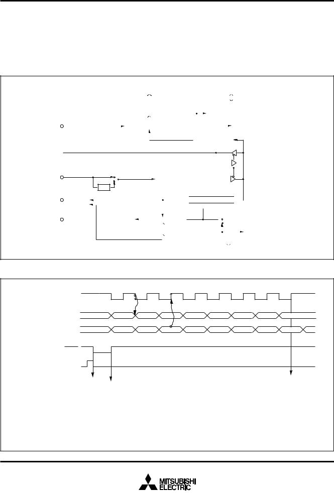
MITSUBISHI MICROCOMPUTERS
3886 Group
SINGLE-CHIP 8-BIT CMOS MICROCOMPUTER
SERIAL I/O
Serial I/O1
Serial I/O1 can be used as either clock synchronous or asynchronous (UART) serial I/O. A dedicated timer is also provided for baud rate generation.
(1) Clock Synchronous Serial I/O Mode
Clock synchronous serial I/O1 mode can be selected by setting the serial I/O1 mode selection bit of the serial I/O1 control register (bit 6 of address 001A16) to “1”.
For clock synchronous serial I/O, the transmitter and the receiver must use the same clock. If an internal clock is used, transfer is started by a write signal to the TB/RB.
|
|
|
|
|
|
|
|
|
|
|
|
|
|
|
|
|
|
|
|
|
|
|
|
Data bus |
|
|
|
|
|
|
|
|
|
|
|
||
|
|
|
|
|
|
|
|
|
|
|
|
|
|
|
|
|
|
|
|
|
|
|
|
|
Address 001816 |
|
Serial I/O1 control register |
Address 001A16 |
|||||||||
|
|
|
|
|
|
|
|
|
|
|
|
|
|
|
||||
|
|
|
|
Receive buffer register |
|
|
|
|
Receive buffer full flag (RBF) |
|||||||||
|
|
|
|
|
|
|
|
|
|
|
|
|
|
Receive interrupt request (RI) |
||||
P44/RXD |
|
|
Receive shift register |
|
|
|
|
|
|
|||||||||
|
|
|
|
|
|
|
|
|||||||||||
|
|
|
|
|
|
Shift clock |
|
|
|
|
|
|
|
|
|
|
||
|
|
|
|
|
|
|
|
|
|
|
|
|
|
|
|
|||
|
|
|
|
|
|
|
Clock control circuit |
|
|
|
|
|||||||
|
|
|
|
|
|
|
|
|
|
|
|
|
|
|||||
P46/SCLK1/OBF10 
BRG count source selection bit
f(XIN)
(f(XCIN) in low-speed mode)
1/4
Serial I/O1 synchronous 
 clock selection bit
  Frequency division ratio 1/(n+1)
Baud rate generator |
|
1/4 |
|
|
|
|
|
||
Address 001C16 |
|
|
|
|
|
|
|
|
|
|
|
|
|
|
|
|
|
|
|
|
P47/SRDY1/S1 |
|
|
F/F |
|
|
|
Falling-edge detector |
|
|
|
|||||
|
|
|
|
|
|
|
|
||||||||
P45/TXD |
|
|
|
|
|
|
|
|
Shift clock |
||||||
|
|
|
|
|
|
|
|
||||||||
|
|
|
|
|
|
|
|||||||||
|
|
|
|
|
|
|
|
|
|||||||
|
|
|
|
|
|
|
|
|
|
||||||
|
|
|
|
|
|
Transmit shift register |
|
||||||||
Clock control circuit 

 Transmit shift completion flag (TSC) Transmit interrupt source selection bit


 Transmit interrupt request (TI)
|
|
|
|
|
|
|
|
|
|
|
|
|
|
Transmit buffer register |
|
|
|
|
Transmit buffer empty flag (TBE) |
||||
|
|
|
|
|
|
||||||
|
|
|
|
|
|
|
|
|
|
||
|
|
|
Address 001816 |
Serial I/O1 status register |
Address 001916 |
||||||
|
|
|
|
|
|
|
|
|
|
||
|
|
|
|
|
|
|
|
|
|
|
|
|
|
Data bus |
|
|
|
|
|
|
|
||
Fig. 21 Block diagram of clock synchronous serial I/O1
Transfer shift clock
(1/2 to 1/2048 of the internal clock, or an external clock)
Serial output TxD
Serial input RxD
Receive enable signal SRDY1
Write pulse to receive/transmit buffer register (address 001816)
D0 |
D1 |
D2 |
D3 |
D4 |
D5 |
D6 |
D7 |
D0 |
D1 |
D2 |
D3 |
D4 |
D5 |
D6 |
D7 |
TBE = 0 |
|
|
RBF = 1 |
|
TSC = 1 |
||||
TBE = 1 |
||||
TSC = 0 |
Overrun error (OE) |
|||
|
|
|
detection |
|
Notes 1: As the transmit interrupt (TI), which can be selected, either when the transmit buffer has emptied (TBE=1) or after the transmit shift operation has ended (TSC=1), by setting the transmit interrupt source selection bit (TIC) of the serial I/O1 control register.
2:If data is written to the transmit buffer register when TSC=0, the transmit clock is generated continuously and serial data is output continuously from the TxD pin.
3:The receive interrupt (RI) is set when the receive buffer full flag (RBF) becomes “1” .
Fig. 22 Operation of clock synchronous serial I/O1 function
26
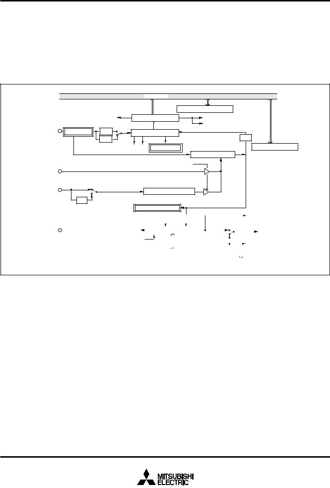
MITSUBISHI MICROCOMPUTERS
3886 Group
SINGLE-CHIP 8-BIT CMOS MICROCOMPUTER
(2) Asynchronous Serial I/O (UART) Mode
Clock asynchronous serial I/O mode (UART) can be selected by clearing the serial I/O1 mode selection bit of the serial I/O1 control register to “0”.
Eight serial data transfer formats can be selected, and the transfer formats used by a transmitter and receiver must be identical.
The transmit and receive shift registers each have a buffer, but the
two buffers have the same address in memory. Since the shift register cannot be written to or read from directly, transmit data is written to the transmit buffer register, and receive data is read from the receive buffer register.
The transmit buffer register can also hold the next data to be transmitted, and the receive buffer register can hold a character while the next character is being received.
|
|
|
Data bus |
|
|
|
|
|
Address 001816 |
|
Serial I/O1 control register Address 001A16 |
|
|
|
|
OE |
Receive buffer register |
Receive buffer full flag (RBF) |
|
|
|
Character length selection bit |
|
Receive interrupt request (RI) |
|
||
P44/RXD |
ST detector |
7 bits |
Receive shift register |
1/16 |
|
|
|
|
8 bits |
|
|
|
|
|
|
|
PE FE |
SP detector |
UART control register |
|
|
|
|
|
|
Clock control circuit |
Address 001B16 |
|
|
Serial I/O1 synchronous clock selection bit |
|
|||
P46/SCLK1/OBF10 |
|
|
|
|
|
|
f(XIN) |
BRG count source selection bit |
Frequency division ratio 1/(n+1) |
|
|||
|
|
Baud rate generator |
|
|||
(f(XCIN) in low-speed mode) |
|
|
||||
|
|
Address 001C16 |
|
|||
|
1/4 |
|
|
|
||
|
|
|
|
|
|
|
|
|
|
ST/SP/PA generator |
|
||
|
|
|
|
|
|
|
|
|
|
|
|
|
|
|
|
|
|
|
|
|
|
Transmit shift completion flag (TSC) |
|||
|
|
|
|
|
|
|
|
|
|
1/16 |
|
|
|
|
|
|
|
|
|
|
|||||
|
|
|
|
|
|
|
|
|
|
|
|
|
|
|
|
|
|
|
|
|
|||||
|
|
|
|
|
|
|
|
|
|
|
|
|
|
|
Transmit interrupt source selection bit |
||||||||||
|
|
|
|
|
|
|
|
|
|
|
|
|
|
|
|||||||||||
P45/TXD |
|
|
Transmit shift register |
|
|
|
|
|
|
|
|
|
|
Transmit interrupt request (TI) |
|||||||||||
|
|
|
|
|
|
||||||||||||||||||||
|
|
|
|
|
|
|
|
|
|
|
|
||||||||||||||
|
|
Character length selection bit |
|
|
|
|
|
|
|
|
|
|
|
|
|
|
|
|
Transmit buffer empty flag (TBE) |
||||||
|
|
|
|
Transmit buffer register |
|
|
|
|
|
|
|
|
|||||||||||||
|
|
|
|
|
|
|
|
|
|
|
|
||||||||||||||
|
|
|
|
|
|
|
|
|
|
|
|
|
|
|
|
Serial I/O1 status register |
Address 001916 |
||||||||
|
|
|
|
|
|
|
|
|
Address 001816 |
|
|||||||||||||||
|
|
|
|
|
|
|
|
|
|
|
|
|
|
|
|
|
|
|
|
||||||
|
|
|
|
|
|
|
|
|
|
|
|
|
|
|
|
|
|
|
|
|
|
|
|
|
|
|
|
|
Data bus |
|
|
|
|
|
|
|
|
|
|
|
|
|
|
|
|
|
|||||
|
|
|
|
|
|
|
|
|
|
|
|
|
|
|
|
|
|
|
|
|
|
|
|
|
|
Fig. 23 Block diagram of UART serial I/O1
27

MITSUBISHI MICROCOMPUTERS
3886 Group
SINGLE-CHIP 8-BIT CMOS MICROCOMPUTER
Transmit or receive clock |
|
|
|
Transmit buffer write |
|
|
|
signal |
|
|
|
TBE=0 |
|
|
TBE=0 |
TSC=0 |
|
|
|
TBE=1 |
|
|
|
Serial output TXD |
ST |
D0 |
D1 |
1 start bit 7 or 8 data bit
1 or 0 parity bit
1 or 2 stop bit (s)
Receive buffer read signal
Serial input RXD |
ST |
D0 |
D1 |
TBE=1 |
|
|
|
TSC=1 |
SP |
ST |
D0 |
D1 |
SP |
|
|
|
Generated at 2nd |
bit in 2-stop-bit mode |
RBF=1 |
|
|
RBF=0 |
|
|
|
|
RBF=1 |
|
SP |
ST |
D0 |
D1 |
SP |
|
|
|
|
Notes 1: Error flag detection occurs at the same time that the RBF flag becomes “1” (at 1st stop bit, during reception).
2:As the transmit interrupt (TI), when either the TBE or TSC flag becomes “1,” can be selected to occur depending on the setting of the transmit interrupt source selection bit (TIC) of the serial I/O1 control register.
3:The receive interrupt (RI) is set when the RBF flag becomes “1.”
4:After data is written to the transmit buffer when TSC=1, 0.5 to 1.5 cycles of the data shift cycle is necessary until changing to TSC=0.
Fig. 24 Operation of UART serial I/O1 function
[Serial I/O1 Control Register (SIO1CON)] 001A16
The serial I/O1 control register consists of eight control bits for the serial I/O function.
[UART Control Register (UARTCON)] 001B16
The UART control register consists of four control bits (bits 0 to 3) which are valid when asynchronous serial I/O is selected and set the data format of an data transfer and one bit (bit 4) which is always valid and sets the output structure of the P45/TXD pin.
[Serial I/O1 Status Register (SIO1STS)] 001916
The read-only serial I/O1 status register consists of seven flags
(bits 0 to 6) which indicate the operating status of the serial I/O function and various errors.
Three of the flags (bits 4 to 6) are valid only in UART mode.
The receive buffer full flag (bit 1) is cleared to “0” when the receive buffer register is read.
If there is an error, it is detected at the same time that data is transferred from the receive shift register to the receive buffer register, and the receive buffer full flag is set. A write to the serial I/O1 status register clears all the error flags OE, PE, FE, and SE (bit 3 to bit 6, respectively). Writing “0” to the serial I/O1 enable bit SIOE
(bit 7 of the serial I/O control register) also clears all the status flags, including the error flags.
Bits 0 to 6 of the serial I/O1 status register are initialized to “0” at reset, but if the transmit enable bit (bit 4) of the serial I/O1 control register has been set to “1”, the transmit shift completion flag (bit
2) and the transmit buffer empty flag (bit 0) become “1”.
[Transmit Buffer Register/Receive Buffer
Register (TB/RB)] 001816
The transmit buffer register and the receive buffer register are located at the same address. The transmit buffer is write-only and the receive buffer is read-only. If a character bit length is 7 bits, the
MSB of data stored in the receive buffer is “0”.
[Baud Rate Generator (BRG)] 001C16
The baud rate generator determines the baud rate for serial transfer.
The baud rate generator divides the frequency of the count source by 1/(n + 1), where n is the value written to the baud rate generator.
28
|
|
|
|
|
|
|
|
|
|
|
|
|
|
|
|
|
|
|
|
|
|
|
|
|
|
|
|
|
|
|
|
|
|
|
|
|
|
|
|
|
|
MITSUBISHI MICROCOMPUTERS |
|
|
|
|
|
|
|
|
|
|
|
|
|
|
|
|
|
|
|
|
|
|
|
|
|
|
|
|
|
|
|
|
|
|
|
|
|
|
|
|
|
|
|
|
|
3886 Group |
|
|
|
|
|
|
|
|
|
|
|
|
|
|
|
|
|
|
|
|
|
|
|
|
|
|
|
|
|
|
|
|
|
|
|
SINGLE-CHIP 8-BIT CMOS MICROCOMPUTER |
|
|||||||||
|
|
|
|
|
|
|
|
|
|
|
|
|
|
|
|
|
|
|
|
|
|
|
|
|
|
|
|
|
|
|
|
|
|
|
|
|
|
|
|
|
|
|
|
|
|
|
|
|
|
|
|
|
|
|
|
|
|||||||||||||||||||||||||||||||||
|
b7 |
|
b0 |
Serial I/O1 status register |
b7 |
|
|
|
b0 |
Serial I/O1 control register |
|
|||||||||||||||||||||||||||||||||
|
|
|
|
|
|
|
|
|
|
|
|
|
|
|
|
|
|
|
|
|
|
|
|
|
|
|
|
|
|
|
|
|
||||||||||||
|
|
|
|
|
|
|
|
|
|
|
|
|
|
|
|
(SIO1STS : address 001916) |
|
|
|
|
|
|
|
|
|
|
|
|
|
|
|
|
(SIO1CON : address 001A16) |
|
||||||||||
|
|
|
|
|
|
|
|
|
|
|
|
|
|
|
|
|
|
|
|
|
|
|
|
|
|
|
|
|
|
|
|
|
||||||||||||
|
|
|
|
|
|
|
|
|
|
|
|
|
|
|
|
|
|
|
|
|
|
|
|
|
|
|
|
|
|
|
|
|
|
|
|
|
|
|
|
|
|
|
|
|
|
|
|
|
|
|
|
|
|
|
|
|
|
|
|
|
|
|
|
|
|
|
|
|
|
|
|
|
|
|
|
|
|
|
|
|
|
|
|
|
|
|
BRG count source selection bit (CSS) |
|
|
|
|
|
|
|
|
|
|
|
|
|
|
|
|
|
|
|
|
|
|
Transmit buffer empty flag (TBE) |
|
|
|
|
|
|
|
|
|
|
|
|
|
|
|
|
|
|
|
|
|
|||
|
|
|
|
|
|
|
|
|
|
|
|
|
|
|
|
|
|
|
|
|
|
|
|
|
|
|
|
|
|
|
|
|
|
|
|
|
|
|
|
|
0: f(XIN) (f(XCIN) in low-speed mode) |
|
||
|
|
|
|
|
|
|
|
|
|
|
|
|
|
|
|
|
|
|
|
0: Buffer full |
|
|
|
|
|
|
|
|
|
|
|
|
|
|
|
|
|
|
|
|
|
|
||
|
|
|
|
|
|
|
|
|
|
|
|
|
|
|
|
|
|
|
|
|
|
|
|
|
|
|
|
|
|
|
|
|
|
|
|
|
|
|
|
|
1: f(XIN)/4 (f(XCIN)/4 in low-speed mode) |
|
||
|
|
|
|
|
|
|
|
|
|
|
|
|
|
|
|
|
|
|
|
1: Buffer empty |
|
|
|
|
|
|
|
|
|
|
|
|
|
|
|
|
|
|
|
|
|
|
||
|
|
|
|
|
|
|
|
|
|
|
|
|
|
|
|
|
|
|
|
|
|
|
|
|
|
|
|
|
|
|
|
|
|
|
|
|
|
|
|
|
|
|
|
|
|
|
|
|
|
|
|
|
|
|
|
|
|
|
|
|
|
|
|
|
Receive buffer full flag (RBF) |
|
|
|
|
|
|
|
|
|
|
|
|
|
|
|
|
|
|
|
|
|
Serial I/O1 synchronous clock selection bit (SCS) |
|
|
|
|
|
|
|
|
|
|
|
|
|
|
|
|
|
|
|
|
|
|
|
|
|
|
|
|
|
|
|
|
|
|
|
|
|
|
|
|
|
|
|||||
|
|
|
|
|
|
|
|
|
|
|
|
|
|
|
|
|
|
|
|
|
|
|
|
|
|
|
|
|
|
|
|
|
|
|
|
|
|
|
|
|
0: BRG output divided by 4 when clock synchronous |
|
||
|
|
|
|
|
|
|
|
|
|
|
|
|
|
|
|
|
|
|
|
0: Buffer empty |
|
|
|
|
|
|
|
|
|
|
|
|
|
|
|
|
|
|
|
|
|
|
||
|
|
|
|
|
|
|
|
|
|
|
|
|
|
|
|
|
|
|
|
|
|
|
|
|
|
|
|
|
|
|
|
|
|
|
|
|
|
|
|
|
serial I/O is selected, BRG output divided by 16 |
|
||
|
|
|
|
|
|
|
|
|
|
|
|
|
|
|
|
|
|
|
|
1: Buffer full |
|
|
|
|
|
|
|
|
|
|
|
|
|
|
|
|
|
|
|
|
|
|
||
|
|
|
|
|
|
|
|
|
|
|
|
|
|
|
|
|
|
|
|
|
|
|
|
|
|
|
|
|
|
|
|
|
|
|
|
|
|
|
|
|
when UART is selected. |
|
||
|
|
|
|
|
|
|
|
|
|
|
|
|
|
|
|
|
|
|
|
|
|
|
|
|
|
|
|
|
|
|
|
|
|
|
|
|
|
|
|
|
|
|
||
|
|
|
|
|
|
|
|
|
|
|
|
|
|
|
|
|
|
|
|
Transmit shift completion flag (TSC) |
|
|
|
|
|
|
|
|
|
|
|
|
|
|
|
|
|
|
|
|
|
1: External clock input when clock synchronous serial |
|
|
|
|
|
|
|
|
|
|
|
|
|
|
|
|
|
|
|
|
|
|
|
|
|
|
|
|
|
|
|
|
|
|
|
|
|
|
|
|
|
|
|
I/O is selected, external clock input divided by 16 |
|
||
|
|
|
|
|
|
|
|
|
|
|
|
|
|
|
|
|
|
|
|
0: Transmit shift in progress |
|
|
|
|
|
|
|
|
|
|
|
|
|
|
|
|
|
|
|
|
|
|
||
|
|
|
|
|
|
|
|
|
|
|
|
|
|
|
|
|
|
|
|
|
|
|
|
|
|
|
|
|
|
|
|
|
|
|
|
|
|
|
|
|
when UART is selected. |
|
||
|
|
|
|
|
|
|
|
|
|
|
|
|
|
|
|
|
|
|
|
1: Transmit shift completed |
|
|
|
|
|
|
|
|
|
|
|
|
|
|
|
|
|
|
|
|
|
|
||
|
|
|
|
|
|
|
|
|
|
|
|
|
|
|
|
|
|
|
|
|
|
|
|
|
|
|
|
|
|
|
|
|
|
|
|
|
|
|
|
|
|
|
|
|
|
|
|
|
|
|
|
|
|
|
|
|
|
|
|
|
|
|
|
|
|
|
|
|
|
|
|
|
|
|
|
|
|
|
|
|
|
|
|
|
|
|
|
output enable bit (SRDY) |
|
|
|
|
|
|
|
|
|
|
|
|
|
|
|
|
|
|
|
|
|
Overrun error flag (OE) |
|
|
|
|
|
|
|
|
|
|
|
|
|
|
|
|
|
|
|
|
|
SRDY1 |
|
|
|
|
|
|
|
|
|
|
|
|
|
|
|
|
|
|
|
|
|
|
|
|
|
|
|
|
|
|
|
|
|
|
|
|
|
|
|
|
|
|
|||||
|
|
|
|
|
|
|
|
|
|
|
|
|
|
|
|
|
|
|
|
|
|
|
|
|
|
|
|
|
|
|
|
|
|
|
|
|
|
|
|
|
0: P47 pin operates as ordinary I/O pin |
|
||
|
|
|
|
|
|
|
|
|
|
|
|
|
|
|
|
|
|
|
|
0: No error |
|
|
|
|
|
|
|
|
|
|
|
|
|
|
|
|
|
|
|
|
|
|
||
|
|
|
|
|
|
|
|
|
|
|
|
|
|
|
|
|
|
|
|
|
|
|
|
|
|
|
|
|
|
|
|
|
|
|
|
|
|
|
|
|
1: P47 pin operates as SRDY1 output pin |
|
||
|
|
|
|
|
|
|
|
|
|
|
|
|
|
|
|
|
|
|
|
1: Overrun error |
|
|
|
|
|
|
|
|
|
|
|
|
|
|
|
|
|
|
|
|
|
|
||
|
|
|
|
|
|
|
|
|
|
|
|
|
|
|
|
|
|
|
|
|
|
|
|
|
|
|
|
|
|
|
|
|
|
|
|
|
|
|
|
|
|
|
|
|
|
|
|
|
|
|
|
|
|
|
|
|
|
|
|
|
|
|
|
|
Parity error flag (PE) |
|
|
|
|
|
|
|
|
|
|
|
|
|
|
|
|
|
|
|
|
|
Transmit interrupt source selection bit (TIC) |
|
|
|
|
|
|
|
|
|
|
|
|
|
|
|
|
|
|
|
|
|
|
|
|
|
|
|
|
|
|
|
|
|
|
|
|
|
|
|
|
|
|
|
||||
|
|
|
|
|
|
|
|
|
|
|
|
|
|
|
|
|
|
|
|
|
|
|
|
|
|
|
|
|
|
|
|
|
|
|
|
|
|
|
|
|
0: Interrupt when transmit buffer has emptied |
|
||
|
|
|
|
|
|
|
|
|
|
|
|
|
|
|
|
|
|
|
|
0: No error |
|
|
|
|
|
|
|
|
|
|
|
|
|
|
|
|
|
|
|
|
|
|
||
|
|
|
|
|
|
|
|
|
|
|
|
|
|
|
|
|
|
|
|
|
|
|
|
|
|
|
|
|
|
|
|
|
|
|
|
|
|
|
|
|
1: Interrupt when transmit shift operation is completed |
|
||
|
|
|
|
|
|
|
|
|
|
|
|
|
|
|
|
|
|
|
|
1: Parity error |
|
|
|
|
|
|
|
|
|
|
|
|
|
|
|
|
|
|
|
|
|
|
||
|
|
|
|
|
|
|
|
|
|
|
|
|
|
|
|
|
|
|
|
|
|
|
|
|
|
|
|
|
|
|
|
|
|
|
|
|
|
|
|
|
|
|
|
|
|
|
|
|
|
|
|
|
|
|
|
|
|
|
|
|
|
|
|
|
Framing error flag (FE) |
|
|
|
|
|
|
|
|
|
|
|
|
|
|
|
|
|
|
|
|
|
Transmit enable bit (TE) |
|
|
|
|
|
|
|
|
|
|
|
|
|
|
|
|
|
|
|
|
|
|
|
|
|
|
|
|
|
|
|
|
|
|
|
|
|
|
|
|
|
|
|
||||
|
|
|
|
|
|
|
|
|
|
|
|
|
|
|
|
|
|
|
|
|
|
|
|
|
|
|
|
|
|
|
|
|
|
|
|
|
|
|
|
|
0: Transmit disabled |
|
||
|
|
|
|
|
|
|
|
|
|
|
|
|
|
|
|
|
|
|
|
0: No error |
|
|
|
|
|
|
|
|
|
|
|
|
|
|
|
|
|
|
|
|
|
|
||
|
|
|
|
|
|
|
|
|
|
|
|
|
|
|
|
|
|
|
|
|
|
|
|
|
|
|
|
|
|
|
|
|
|
|
|
|
|
|
|
|
1: Transmit enabled |
|
||
|
|
|
|
|
|
|
|
|
|
|
|
|
|
|
|
|
|
|
|
1: Framing error |
|
|
|
|
|
|
|
|
|
|
|
|
|
|
|
|
|
|
|
|
|
|
||
|
|
|
|
|
|
|
|
|
|
|
|
|
|
|
|
|
|
|
|
|
|
|
|
|
|
|
|
|
|
|
|
|
|
|
|
|
|
|
|
|
|
|
|
|
|
|
|
|
|
|
|
|
|
|
|
|
|
|
|
|
|
|
|
|
Summing error flag (SE) |
|
|
|
|
|
|
|
|
|
|
|
|
|
|
|
|
|
|
|
|
|
Receive enable bit (RE) |
|
|
|
|
|
|
|
|
|
|
|
|
|
|
|
|
|
|
|
|
|
|
|
|
|
|
|
|
|
|
|
|
|
|
|
|
|
|
|
|
|
|
|
||||
|
|
|
|
|
|
|
|
|
|
|
|
|
|
|
|
|
|
|
|
|
|
|
|
|
|
|
|
|
|
|
|
|
|
|
|
|
|
|
|
|
0: Receive disabled |
|
||
|
|
|
|
|
|
|
|
|
|
|
|
|
|
|
|
|
|
|
|
0: (OE) U (PE) U (FE)=0 |
|
|
|
|
|
|
|
|
|
|
|
|
|
|
|
|
|
|
|
|
|
|
||
|
|
|
|
|
|
|
|
|
|
|
|
|
|
|
|
|
|
|
|
|
|
|
|
|
|
|
|
|
|
|
|
|
|
|
|
|
|
|
|
|
1: Receive enabled |
|
||
|
|
|
|
|
|
|
|
|
|
|
|
|
|
|
|
|
|
|
|
1: (OE) U (PE) U (FE)=1 |
|
|
|
|
|
|
|
|
|
|
|
|
|
|
|
|
|
|
|
|
|
|
||
|
|
|
|
|
|
|
|
|
|
|
|
|
|
|
|
|
|
|
|
|
|
|
|
|
|
|
|
|
|
|
|
|
|
|
|
|
|
|
|
|
|
|
|
|
|
|
|
|
|
|
|
|
|
|
|
|
|
|
|
|
|
|
|
|
Not used (returns “1” when read) |
|
|
|
|
|
|
|
|
|
|
|
|
|
|
|
|
|
|
|
|
|
Serial I/O1 mode selection bit (SIOM) |
|
|
|
|
|
|
|
|
|
|
|
|
|
|
|
|
|
|
|
|
|
|
|
|
|
|
|
|
|
|
|
|
|
|
|
|
|
|
|
|
|
|
|
||||
|
|
|
|
|
|
|
|
|
|
|
|
|
|
|
|
|
|
|
|
|
|
|
|
|
|
|
|
|
|
|
|
|
|
|
|
|
|
|
|
|
0: Clock asynchronous (UART) serial I/O |
|
||
|
|
|
|
|
|
|
|
|
|
|
|
|
|
|
|
|
|
|
|
|
|
|
|
|
|
|
|
|
|
|
|
|
|
|
|
|
|
|
|
|
|
|
||
|
|
|
|
|
|
|
|
|
|
|
|
|
|
|
|
|
|
|
|
|
|
|
|
|
|
|
|
|
|
|
|
|
|
|
|
|
|
|
|
|
|
1: Clock synchronous serial I/O |
|
|
|
|
|
|
|
|
|
|
|
|
|
|
|
|
|
|
|
|
|
|
|
|
|
|
|
|
|
|
|
|
|
|
|
|
|
|
|
|
|
|
|
|
|||
|
|
|
|
|
|
|
|
|
|
|
|
|
|
|
|
|
|
|
|
|
|
|
|
|
|
|
|
|
|
|
|
|
|
|
|
|
|
|
|
|
|
Serial I/O1 enable bit (SIOE) |
|
|
|
|
|
|
|
|
|
|
|
|
|
|
|
|
|
|
|
|
|
|
|
|
|
|
|
|
|
|
|
|
|
|
|
|
|
|
|
|
|
|
|
|
|
||
|
|
|
|
|
|
|
|
|
|
|
|
|
|
|
|
|
|
|
|
|
|
|
|
|
|
|
|
|
|
|
|
|
|
|
|
|
|
|
|
|
|
0: Serial I/O disabled |
|
|
|
b7 |
|
b0 |
UART control register |
|
|
|
|
|
|
|
|
|
|
|
|
|
|
|
|
|
|
|
|
(pins P44 to P47 operate as ordinary I/O pins) |
|
||||||||||||||||||
|
|
|
|
|
|
|
|
|
|
|
|
|
|
|
|
(UARTCON : address 001B16) |
|
|
|
|
|
|
|
|
|
|
|
|
|
|
|
|
|
|
|
|
1: Serial I/O enabled |
|
||||||
|
|
|
|
|
|
|
|
|
|
|
|
|
|
|
|
|
|
|
|
Character length selection bit (CHAS) |
|
|
|
|
|
|
|
|
|
|
|
|
|
|
|
|
|
|
|
|
(pins P44 to P47 operate as serial I/O pins) |
|
||
|
|
|
|
|
|
|
|
|
|
|
|
|
|
|
|
|
|
|
|
|
|
|
|
|
|
|
|
|
|
|
|
|
|
|
|
|
|
|
|
|
|
|
||
|
|
|
|
|
|
|
|
|
|
|
|
|
|
|
|
|
|
|
|
|
|
|
|
|
|
|
|
|
|
|
|
|
|
|
|
|
|
|
|
|
|
|
||
|
|
|
|
|
|
|
|
|
|
|
|
|
|
|
|
|
|
|
|
0: 8 bits |
|
|
|
|
|
|
|
|
|
|
|
|
|
|
|
|
|
|
|
|
|
|
|
|
|
|
|
|
|
|
|
|
|
|
|
|
|
|
|
|
|
|
|
|
1: 7 bits |
|
|
|
|
|
|
|
|
|
|
|
|
|
|
|
|
|
|
|
|
|
|
|
|
Parity enable bit (PARE)
0:Parity checking disabled
1:Parity checking enabled
Parity selection bit (PARS)
0:Even parity
1:Odd parity
Stop bit length selection bit (STPS)
0:1 stop bit
1:2 stop bits
P45/TXD P-channel output disable bit (POFF)
0:CMOS output (in output mode)
1:N-channel open drain output (in output mode)
Not used (return “1” when read)
Fig. 25 Structure of serial I/O1 control registers
29
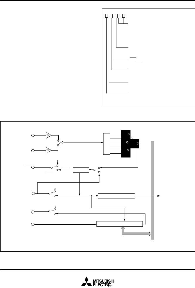
MITSUBISHI MICROCOMPUTERS
3886 Group
SINGLE-CHIP 8-BIT CMOS MICROCOMPUTER
Serial I/O2
b7 |
b0 |
The serial I/O2 function can be used only for clock synchronous serial I/O.
For clock synchronous serial I/O the transmitter and the receiver must use the same clock. If the internal clock is used, transfer is started by a write signal to the serial I/O2 register.
[Serial I/O2 Control Register (SIO2CON)] 001D16
The serial I/O2 control register contains seven bits which control
various serial I/O functions.
Serial I/O2 control register (SIO2CON : address 001D16)
Internal synchronous clock selection bits
b2 b1 b0
0 0 0: f(XIN)/8 (f(XCIN)/8 in low-speed mode)
00 1: f(XIN)/16 (f(XCIN)/16 in low-speed mode)
01 0: f(XIN)/32 (f(XCIN)/32 in low-speed mode)
01 1: f(XIN)/64 (f(XCIN)/64 in low-speed mode)
11 0: f(XIN)/128 (f(XCIN)/128 in low-speed mode)
11 1: f(XIN)/256 (f(XCIN)/256 in low-speed mode)
Serial I/O2 port selection bit
0:I/O port
1:SOUT2,SCLK2 signal output
SRDY2 output enable bit
0:I/O port
1:SRDY2 signal output
Transfer direction selection bit
0:LSB first
1:MSB first
Serial I/O2 synchronous clock selection bit
0:External clock
1:Internal clock
Comparator reference input selection bit
0:P00/P3REF input
1:Reference input fixed
Fig. 26 Structure of serial I/O2 control register
|
|
|
|
|
Internal synchronous |
|
|
|
|
|
1/8 |
clock selection bits |
|
XCIN |
|
|
|
|
|
|
Main clock divide ratio “10” |
|
|
1/16 |
|
Data bus |
|
|
|
Divider |
1/32 |
|
||
|
|
|
|
|||
|
selection bits (Note) |
|
1/64 |
|
|
|
|
|
|
|
|
||
|
|
|
|
|
|
|
|
“00” |
|
|
1/128 |
|
|
XIN |
“01” |
|
|
1/256 |
|
|
|
P73 latch |
|
|
|
|
|
|
Serial I/O2 synchronous |
|
|
|
|
|
P73/SRDY2 |
“0” |
clock selection bit “1” |
|
|
|
|
SRDY2 |
Synchronization |
|
|
|
|
|
/INT21 |
“1” |
circuit |
|
|
|
|
|
SRDY2 output enable bit |
SCLK2 |
“0” |
|
|
|
|
|
|
|
|
|
|
|
|
External clock |
|
|
|
|
|
P72 latch |
|
|
|
|
|
|
“0” |
|
|
|
|
|
P72/SCLK2 |
|
|
Serial I/O counter 2 (3) |
|
||
|
“1” |
|
|
|||
|
Serial I/O2 port selection bit |
|
|
|
|
|
|
P71 latch |
|
|
|
|
|
|
“0” |
|
|
|
|
|
P71/SOUT2 |
|
|
|
|
|
|
|
“1” |
|
|
|
|
|
|
Serial I/O2 port selection bit |
|
|
|
|
|
P70/SIN2 |
|
|
Serial I/O2 register (8) |
|
||
|
|
|
|
|
|
|
Serial I/O2 interrupt request
Note: These are assigned to bits 7 and 6 of the CPU mode register (address 003B16).
These bits select any of the high-speed mode, the middle-speed mode, and the low-speed mode.
Fig. 27 Block diagram of serial I/O2 function
30
Loading...