


 Loading...
MONITOR WITH DVD RECEIVER / NAVIGATION SYSTEM
DDX7032/7032M/712
DNX7120/7220/7320
SERVICE MANUAL
© 2008-4 PRINTED IN JAPAN B53-0634-00 (N) 429
Illustrations is DNX7120
NAVIGATION SYSTEM |
DNX7120 |
ANT module(GPS-ANT)* Mounting hardware* (W02-5305-05) (J21-9867-04)
(5m) |
|
Screw set * |
Adhesive double- |
(N99-1779-15) |
coated tape * |
|
(H30-0595-04) |
|
|
|
|
Clamper * |
|
|
|
|
|
(J11-0660-05) |
|
DC cord * |
DC cord * |
Cord with pinplug(AV) Cord with pinplug(PRE) |
|
||
(E30-6825-05) |
(E30-6824-05) |
(E30-6792-05) |
(E30-6794-05) |
|
|
|
|
|
|
Cord with plug(ipod)* |
Cord with plug(relay) |
|
|
|
|
(E30-6785-05) |
(E30-6786-05) |
PRK: (2m) |
|
|
|
|
|
REV: (5m) |
|
|
(1m) |
(1m) |
|
Remote controller assy |
|
Escutcheon |
Escutcheon * |
Mounting hardware assy |
Lever |
(A70-2082-15) RC-DV330 :DNX |
(B07-3224-01) |
(B07-3172-12) |
(J22-0657-03) |
(D10-4589-04) x2 |
|
(A70-2083-15) RC-DV340 :DDX
Size AAA battery
Not supplied
ILLUSTRATION IS
RC-DV340
 The IC106 in the Digital I/O unit (X88-2030-11) are not replaceable components. When this IC are defective, replace the whole Digital I/O unit (X88-2030-11).
 The IC5,9,21 and IC60 in the DVD unit (X37-1120-06) are not replaceable components. When these ICs are defective, replace the whole DVD mechanism assembly (X92-6180-01). You cannot replace only the board.
* Depends on the models. Refer to the parts list.
This product uses Lead Free solder.
This product complies with the RoHS directive for the European market.

DDX7032/7032M/712 |
|
|
|
|
|
|
|
|
|
|
|||
DNX7120/7220/7320 |
|
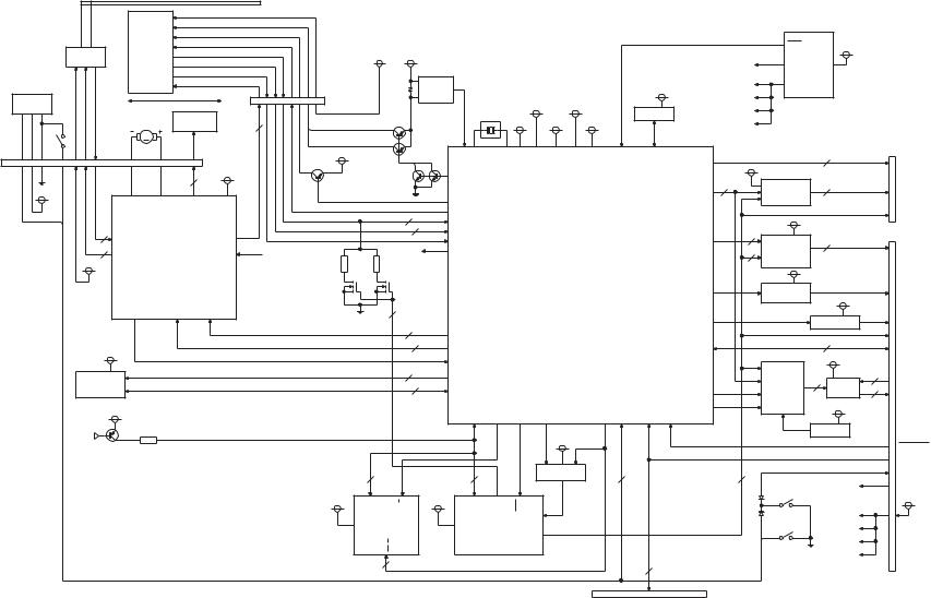
BLOCK DIAGRAM |
|
||||||||||
|
|
|
|
|
|
||||||||
(X88- ) |
USB I/F |
|
|
(X15- ) (A/2) |
|
|
iPod |
|
|
|
MIC |
|
S/PDIF |
CN101 |
J502 |
|
|
|
J501 |
|
|
J500 |
J503 |
||||
IC106 |
|
|
|
|
|
|
|
|
|
|
|
|
|
MEDIA PROCESSOR |
|
|
|
ISO |
ISO |
|
|
|
|
|
CN701 |
||
|
|
|
|
|
|
|
|
|
|
|
|||
|
HSY |
|
|
|
|
AMP |
AMP |
|
|
|
|
|
|
IC302 |
IC104 VSY IC901 |
|
|
|
|
|
|
|
|
|
|
|
|
VIDEO |
CSYNC |
AUDIO |
|
|
|
|
|
|
|
|
|
|
|
ENC |
GEN |
DAC |
|
|
|
|
|
|
|
|
|
|
|
CN328 |
|
|
|
|
|
|
|
|
|
|
|
DDX8xx/ |
|
|
|
|
|
|
|
|
|
|
|
|
IC500 |
|
|
|
|
|
|
|
BT xx |
|
|
|
|
|
DNX8xx ONLY |
|
|
|
|
|
CN851 |
|
|
|
|
|
|
BT |
|
||
|
|
|
|
|
|
|
|
|
|
|
IC502 |
||
|
|
|
EP xx |
|
|
|
|
|
|
|
|
BT L/R |
|
|
|
|
|
|
|
|
|
|
|
|
|
||
|
|
|
BT xx |
|
|
|
|
|
|
|
|
|
|
|
|
|
|
|
|
|
|
|
|
|
iPod L/R |
|
|
|
|
|
|
|
|
|
|
|
|
|
|
|
|
|
|
USB L/R |
|
|
|
|
|
|
|
|
USB L/R |
AUDIO |
|
|
GUI CSYNC |
|
|
|
|
|
|
|
|
|
DVD-A L/R |
SELECT |
|
|
|
|
|
|
|
|
|
|
|
|
|
||
GUI RGB |
|
|
|
|
|
|
|
|
|
|
|
IC505 |
|
|
|
|
|
|
|
|
|
|
|
|
|
|
|
|
|
|
|
|
|
|
|
|
|
|
|
|
AUDIO |
|
|
|
|
|
|
|
|
|
|
|
|
|
SELECT |
|
|
|
|
|
|
DDX8xx/ |
|
|
|
|
|
|
|
|
CN852 |
|
|
|
|
DDX7xx |
|
|
|
|
|
|
|
|
|
DVD SCL/SDA,DISC DET |
|
ONLY |
|
|
|
|
|
MIX REMO INV |
|||
|
|
|
|
|
|
|
|
|
|
||||
|
|
S/PDIF |
|
|
|
|
|
|
|
|
|
|
X34 VIDEO |
|
|
|
|
|
|
|
|
|
|
|
|
|
|
|
|
|
|
|
|
|
|
|
|
|
|
|
X15 VIDEO |
|
|
A MUTE |
|
|
|
|
|
|
|
|
|
W REMO |
|
DVD |
|
|
|
|
|
|
|
|
|
|
|
|
RESET |
MECHA |
|
|
AUDIO |
|
|
|
|
|
|
|
|
|
ACC RST |
|
|
|
|
|
|
|
|
|
|
|
|
||
|
|
|
MUTE |
|
|
|
|
|
|
|
|
|
|
|
|
|
|
|
|
|
|
|
|
|
|
|
BU DET |
|
|
|
|
|
DVD VIDEO |
iPod VIDEO X34 VIDEO |
X15 VIDEO |
GUI CSYNC |
NAVI CSYNC |
|
AOUT SW1/2 AOUT SW3/MUTE |
|
BU DET |
|
|
|
|
|
SYS xx |
|
IC700 |
||||||
|
|
|
|
|
M,P |
MOTOR |
|||||||
|
|
|
|
|
DRIVER |
||||||||
|
|
|
|
|
VIDEO |
|
|
|
|
|
TMOROR |
|
|
|
|
|
|
|
SELECT |
|
|
|
|
|
|||
|
|
|
|
|
IC609 |
|
|
|
|
|
|
||
|
|
|
|
|
|
|
|
|
|
|
|
||
|
|
|
|
|
DET,EP |
|
|
|
|
|
|
|
CN700 |
|
|
|
|
|
|
|
|
|
|
|
|
|
|
|
|
|
|
|
DVD SCL/SDA,DISC |
|
|
|
|
|
|
|
INV PWM, |
|
|
|
|
|
|
|
|
|
|
|
|
PWM,etc |
|
|
|
|
DVD RGB GUI RGB X34 RGB |
|
|
|
|
|
|
|
MONI VIDEO |
||
|
|
|
IC600 |
RGB |
|
|
|
|
|
|
|
|
MONI RGB |
|
|
|
601 |
SELECT |
|
|
IC606 |
|
|
|
|
I2C,etc |
|
|
|
|
|
|
|
|
|
|
|
|
|||
|
|
|
|
|
|
|
|
|
|
|
|
||
|
|
|
|
|
TX/RX,etc |
|
|
SYNC |
|
|
|
X35 HD |
|
|
|
|
|
|
SW2/3 |
|
SEPA |
|
|
|
|
||
|
|
|
|
|
|
|
SW2 |
DET |
|
|
|
||
(X15- ) |
|
|
|
IC404 |
NAVI |
RGB |
|
|
RGB |
ACC |
|
CONT |
|
(B/2) |
CN501 |
|
|
|
|
|
|
|
|||||
|
|
|
|
|
|
|
|
|
|
X35 |
|
||
|
|
|
|
|
|
|
|
|
|
|
|
||
DISC |
|
SW5V |
|
|
|
|
|
|
|
|
|
LED PWM |
|
|
SW |
|
|
|
|
|
|
|
|
|
|||
|
|
|
|
|
|
|
|
|
|
|
|
||
LED |
|
|
LED ON |
|
|
|
|
|
|
|
|
|
|
|
|
|
|
|
|
|
|
|
|
|
|
||
|
|
|
|
|
|
|
|
|
|
|
|
|
REMO |
|
|
|
ROM |
I2C |
|
SYSTEM |
|
|
|
SYS RST |
|
KEY RST |
|
|
|
|
|
|
u-COM |
|
|
|
|
IC402 |
|
||
|
CN500 |
|
|
|
|
|
|
|
|
|
|||
|
|
|
|
|
|
|
|
|
|
|
|
||
|
|
|
|
|
|
|
|
|
|
|
RESET |
|
|
|
|
TXD/RXD,SCLK,etc |
|
|
|
|
|
|
|
|
|
||
|
|
|
|
|
|
|
|
|
|
|
|
IC |
|
u-COM |
KEY3,SRC,LED PWM,etc |
|
WRITE |
|
|
SI |
SW |
SI (3.3V) |
|
|
DC CN
(X34- )
ACC
ACC
DET
CN350
ACC DET
NAVI RGB
NAVI SYNC
NAVI TX/RX,etc
S/PDIF
SYS xx
MIX REMO INV
X34 VIDEO
X15 VIDEO
W REMO
RESET
ACC RST
BU DET
BU+14.4V |
|
TILT M+/- |
|
(X35- ) (A/2) |
|
CN100 |
Q500- |
X/YDATA,etc |
TOU |
IC1 |
CIRC |
|
|
INVERTER |
|
CIRCUIT |
|
|
IC30 |
FILTER |
|
|
TIM |
|
CO |
|
VID |
|
DE |
|
GA |
Q600 |
CN60 |
SW |
|
SI (3.3V) |
|
REMO |
|
KEY RST |
|
(X35- ) (B/2) |
|
2

|
|
|
|
|
|
|
|
|
|
|
|
|
|
|
|
|
|
DDX7032/7032M/712 |
||||
|
|
|
|
|
|
|
BLOCK DIAGRAM |
|
|
|
DNX7120/7220/7320 |
|||||||||||
|
|
|
|
|
|
|
|
|
|
|
|
|
|
|
||||||||
|
|
|
|
DNX8xx/DNX7xx ONLY |
|
|
DDX8xx/DNX8xx ONLY |
|
|
|
|
|
|
|
DDX812/8032BT/ |
|
|
|||||
|
|
|
|
|
|
(X16-636) |
(X17- ) |
|
|
|
|
|
|
|
|
|
|
|||||
|
|
DDX8xx/ |
|
|
|
|
|
|
|
|
|
|
DNX8120/ |
|
|
|
||||||
|
|
DDX7xx ONLY |
|
|
|
|
IC6 |
IC7 |
|
|
|
|
|
DDX7xx/DNX7xx |
DNX8220BT/ |
|||||||
|
|
|
|
|
|
|
|
|
|
|
|
|
|
ONLY |
|
|
||||||
|
|
|
|
|
NAVI |
2 |
SD |
|
DSPxx |
|
|
|
|
|
|
DNX7220 ONLY |
||||||
|
|
|
NAVI I/F |
|
|
|
DSP |
|
|
|
|
|
|
|
||||||||
|
|
|
|
|
SLOT |
|
|
|
|
|
|
|
|
|
MINI DIN |
|
|
|||||
|
|
|
|
|
|
|
|
|
CODEC |
|
CODECxx |
|
CODECxx, |
|
|
|
|
ANT. |
|
ANT. |
||
|
|
|
|
|
|
|
|
|
|
|
|
|
DSPxx,etc |
|
|
|
|
|
|
|
||
|
|
|
|
|
|
|
|
|
|
|
|
|
|
|
|
|
|
|
|
|
||
|
DC CN |
|
|
|
|
TV I/F |
S/PDIF |
|
|
|
BM |
|
|
|
|
|
|
|
|
|
|
|
|
|
|
|
|
|
|
|
|
|
|
|
|
|
|
|
|
|
|
||||
|
|
|
|
|
|
|
|
ADC L/R |
|
DAC 6ch |
|
|
|
|
J650 |
|
W500 |
W1 |
||||
|
SP OUT |
|
|
|
|
|
|
|
|
|
|
|
|
|
|
CN1 |
|
|
|
|
(X89- ) |
|
|
|
|
|
|
TV xx |
|
|
|
|
|
|
|
|
|
|
|
|
|
|
|
||
|
NAVI |
TX/RX |
|
NAVI TX/RX, etc |
|
|
|
|
|
|
|
|
|
CN900 |
|
SAT TX/RX,etc |
|
|
|
|||
C |
|
|
|
|
|
|
DAC 6ch |
|
|
|
|
|
|
|
|
CN2 |
||||||
T |
IC704 |
|
|
|
|
ADC L/R |
|
|
|
|
CODECxx, DSPxx,etc |
|
|
|
|
|
|
|||||
|
|
DC DET |
|
|
|
|
|
|
|
|
|
|
|
|
||||||||
|
PWIC |
|
|
|
|
|
|
|
|
|
|
|
|
|
|
|||||||
|
|
|
|
|
|
|
|
IC203 |
|
|
|
|
|
|
||||||||
|
|
|
|
|
|
|
|
|
PREFL/R |
|
|
|
||||||||||
|
|
|
|
|
|
|
|
|
|
|
|
|
|
|
|
|
|
|
|
|||
|
|
|
|
|
DET MUTE |
|
|
|
|
|
|
|
|
|
|
PRER L/R |
|
|
|
|
||
|
|
|
|
|
|
|
|
|
|
E-VOL |
|
|
|
PREF S/C |
|
|
|
|
||||
|
|
|
|
|
|
|
|
|
|
|
|
|
|
|
|
|
|
|
|
|||
etc |
|
|
|
|
|
|
|
|
|
|
|
|
|
|
I2C |
|
|
|
|
|
|
|
|
|
|
|
|
|
|
|
|
|
|
|
|
|
|
|
|
|
|
|
|
|
|
|
|
|
|
|
NAVI L/R |
|
|
|
L/R |
L/R |
|
|
|
|
|
TUNE L/R |
|
|
|
|
||
|
|
|
REMO |
|
|
|
|
|
|
|
|
|
|
MUTExxA |
|
|
|
|
|
|
||
|
|
|
|
|
|
|
|
MAIN |
SUB |
|
|
|
SAT L/R |
|
|
|
|
TUN xx, |
F/E |
|
||
|
|
|
|
|
|
|
|
|
|
|
|
|
|
|
|
|
RADIO |
|||||
|
|
|
|
|
|
|
|
|
|
|
|
|
|
|
|
|
etc |
|
|
|||
|
|
|
MIX |
|
|
|
|
|
IC200 |
|
|
|
|
|
|
IC702 |
|
|
|
|
||
|
|
|
|
|
|
TV L/R |
|
|
|
|
|
|
|
|
|
|
|
|
||||
|
|
|
|
|
|
|
|
|
|
|
|
|
|
|
|
|
|
|
IC500 |
|
||
|
|
|
|
|
|
|
|
|
|
|
|
|
|
|
|
|
|
|
|
|
||
|
|
|
|
|
|
|
TV VIDEO |
|
|
|
|
|
|
|
|
|
|
|
|
R xx, |
|
|
|
|
|
|
|
|
|
|
AV SELECTOR |
|
|
|
|
|
|
|
RDS |
|
|||||
|
|
|
|
|
|
|
NAVI COMP |
|
I2C |
|
|
|
|
|
etc |
WRITE |
||||||
|
|
|
|
|
|
|
|
|
|
|
|
|
|
|
|
|
|
|||||
|
|
|
|
|
|
|
X15 MAIN L/R |
ISO AMP |
|
|
|
AUDIO |
|
|
|
SAT TX/RX,etc |
||||||
|
|
|
|
|
|
|
X15 SUB L/R |
|
|
|
|
|
|
|||||||||
|
|
|
|
|
|
|
|
|
|
|
|
|
|
|
||||||||
|
|
|
|
|
|
|
|
|
|
|
|
|
|
|
u-COM |
|
|
|
A RESET |
u-COM |
||
|
|
|
|
|
|
|
|
|
|
|
|
|
|
|
|
|
|
|
|
|||
|
|
|
|
|
PWIC xx |
|
|
|
|
|
|
|
|
|
|
|
|
|
|
|
|
|
|
|
|
|
|
|
|
|
|
|
|
|
|
|
|
|
|
|
|
|
|
|
|
NV |
|
|
|
|
|
|
|
|
AVIN2 VIDEO |
AVIN1 VIDEO AVIN2 L/R |
BCAM VIDEO |
AVOUT VIDEO |
AVOUT L/R AVIN1 L/R |
|
|
AV OUT A MUTE |
|
|
PRE OUT A MUTE |
RELAY SW |
|
|
|
|
|
|
|
|
|
|
|
|
|
|
|
|
|
||||||||
|
|
|
|
|
IC701 |
|
|
|
|
|
|
|
|
|
|
|
|
|
|
|
|
|
|
|
|
|
|
RESET |
|
|
|
|
|
|
|
|
|
|
|
|
|
|
|
|
|
|
|
|
|
|
IC |
|
|
|
|
|
|
|
|
|
|
|
|
|
|
|
|
|
|
|
|
|
|
|
|
|
DET MUTE |
|
|
|
|
|
|
|
|
|
|
|
|
|
|
|
|
|
|
|
|
|
CN401 |
|
|
|
|
|
|
|
|
|
|
|
CN400 |
|
|
|
tc |
Q500-504 |
|
|
CN500 |
|
|
(X29- ) |
|
WH1 |
|
|
|
|
|
|
|
|
|
|
CN300 |
|
|
TOUCH |
|
|
|
TOUCH |
|
|
|
|
|
|
|
|
|
|
|
|
|
|
|
|
||
|
CIRCUIT |
|
|
CN1 |
PANEL |
|
|
|
DET MUTE |
|
|
|
|
AVOUT L/R |
|
AV OUT A MUTE |
PREF S/C PRER L/R PREF L/R |
OUT A MUTE |
RELAY SW |
|
|
|
|
|
|
|
|
|
|
|
|
|
|
|
|
|
|
|
|
||||||
TER |
|
|
|
|
BACK |
|
|
|
|
|
|
|
|
AV OUT |
|
|
||||||
IT |
|
|
|
|
LIGHT |
|
|
|
|
|
|
|
|
|
|
|||||||
|
IC301 |
|
|
|
|
|
|
M+/- |
|
|
|
|
|
A MUTE |
|
|
||||||
R |
|
|
|
|
|
|
|
|
|
|
|
|
|
|
|
|
|
PRE |
|
|
|
|
|
|
|
|
|
|
|
|
|
|
|
|
|
|
|
|
|
|
|
|
|
||
|
TIMING |
|
|
CN301 |
|
|
|
TILT |
|
|
|
|
|
|
|
PRE OUT A MUTE |
RELAY |
|
||||
|
|
|
|
|
|
|
|
|
|
|
|
|
SW |
|
||||||||
|
CONTROLLER/ |
|
|
|
|
|
|
|
|
|
|
|
|
|
|
|
|
|
||||
|
VIDEO |
|
|
|
LCD |
|
|
|
|
|
|
|
|
|
|
|
|
|
|
DDX8xx/ |
|
|
|
DECODER/ |
|
|
|
|
|
|
|
|
|
|
BCAM VIDEO |
AVOUT VIDEO AVOUT L/R |
|
IC100- |
|
|
|
|
|||
|
|
|
|
PANEL |
|
|
|
AVIN2 VIDEO |
|
AVIN1 VIDEO |
|
|
|
|
DNX8xx |
|
|
|||||
|
GAMMA |
|
|
|
|
|
|
|
|
|
102 |
|
|
|
|
|
||||||
|
|
|
|
|
|
|
|
AVIN2 L/R |
AVIN1 L/R |
|
|
|
|
ONLY |
|
|
||||||
|
|
|
|
|
|
|
|
|
|
|
5V PRE OUT |
|
|
|||||||||
|
|
|
|
|
|
|
|
|
|
|
|
|
|
|||||||||
|
|
|
|
|
|
|
|
|
|
|
|
|
|
|
|
|
||||||
|
(X16-628) |
|
|
|
|
|
CN302 |
|
|
|
|
|
|
|
|
|
|
|
|
|
||
|
CN600 |
LED 9V |
|
|
|
|
|
DDX8xx/ DNX8xx AVIN 2 ONLY |
DDX7xx/ DNX7xx AVIN 1 ONLY |
BACK CAM |
AV OUT |
|
|
SUB SUB/CENT |
REAR L/R |
FRONT L/R |
RELAY |
|
||||
|
|
|
|
|
|
|
DDX7xx/ DDX8xx/ DNX7xx DNX8xx ONLY ONLY |
|
||||||||||||||
|
|
LED |
|
|
|
|
|
|
|
|||||||||||||
|
|
|
|
|
|
TILT |
|
|
|
|
||||||||||||
|
|
|
|
|
|
|
|
|
|
|
||||||||||||
|
|
|
|
|
|
|
MECHA |
|
|
|
|
|||||||||||
|
|
|
DSI |
|
|
|
|
|
|
|
|
|||||||||||
|
|
REMO |
REMO |
|
|
|
|
|
|
|
||||||||||||
|
|
|
|
|
|
|
|
|
|
|
||||||||||||
|
|
KEY RST |
RESET |
|
|
|
|
|
|
|
||||||||||||
|
|
|
|
|
|
|
|
|
|
|
||||||||||||
|
KEY3,SRC,etc |
|
|
|
|
|
|
|
|
|||||||||||||
|
SW |
|
|
|
|
|
|
|
|
|
|
|
|
|
|
|
|
|
|
|||
|
|
|
|
|
|
|
|
|
|
|
|
|
|
|
|
|
|
|
|
|
|
|
|
|
|
|
BT |
|
|
|
|
|
|
|
|
|
|
|
|
|
|
|
|
|
|
|
|
|
|
ANT |
|
|
|
|
|
|
|
|
|
|
|
|
|
|
|
|
|
|
|
|
|
|
|
|
|
|
|
|
|
|
|
|
|
|
|
|
|
|
|
|
3 |
4
(X37-112) |
|
|
|
|
|
DISC |
|
|
||
|
|
|
|
|
|
|
|
PDIC VCC |
|
|
|
|
|
|
|
|
|
|
DVD LD/CD LD |
|
|
|
|
|
|
|
|
|
|
HFM |
|
|
|
|
|
|
|
KDP2C |
|
|
VREFH |
|
|
|
|
|
|
|
|
|
|
|
|
|
|
|
SPINDLE |
OPTICAL |
|
IMON/VR DVD/VR CD |
|||||
|
|
MOTOR |
PICKUP |
|
PDIC I/V OUT |
|
||||
|
|
BIAS |
COIL |
SENSOR |
|
|
|
THERMISTER |
|
|
|
|
|
|
|
FO+-,TR+- |
|
||||
HALL IC |
HALL |
U.V.W |
HALL |
LO/EJ |
|
|
|
|
|
|
|
|
|
|
|
|
|
|
|
||
|
|
|
|
|
DC MOTOR |
2PHASE |
|
|||
|
SW |
|
|
|
STEPPING |
4 |
||||
|
|
|
|
|
|
|
||||
|
|
|
|
M |
|
|
|
|
|
|
|
LIM- |
|
|
|
|
|
|
|
CONNECTOR |
|
|
|
|
|
|
|
|
|
|
||
|
|
|
|
|
|
|
|
|
(28P) |
P5V |
|
|
|
|
|
|
|
|
4 |
|
|
|
|
|
|
|
|
|
|
|
|
|
SW EIEND |
D3.3V |
|
|
|
IC10 |
|
|
|
|
|
|
|
|
|
|
|
|
|
|
||
|
|
|
|
|
FO6,RO6 |
|
FO4,RO4 |
FO5,RO5 |
|
|
|
|
|
|
3 |
H1H,H1L,HB |
|
|
|
FO2,RO2 |
|
|
|
|
|
|
|
|
|
FO3,RO3 |
|
|
|
|
|
|
3 |
A1,A2,A3 |
MOTOR & |
VREF,EC |
VHALF |
||
|
|
|
|
|
|
|||||
|
|
|
|
P5V |
|
ACTUATER |
|
|||
|
|
|
|
|
DRIVER |
|
|
|||
|
|
|
|
|
|
|
|
|||
|
|
|
|
|
|
|
|
SPIN,IN2-6,MUTE |
|
|
|
|
|
|
|
FG |
|
|
BMS |
STBY |
|
D3.3V
IC54
SDRAM
D3.3V
Q25
IF-SEL |
EXADT11 |
A5V |
A5V |
|
|
|
|
IC39 |
|
CONNECTOR |
|
IOPDET |
|
|
|
|
|
(30P) |
|
A3.3V |
V3.3V |
Q12,13 |
27MHz |
|
|
D3.3V PLL3.3V D1.2V |
|||
IC1
A3.3V
Q27
Q14,15
|
16 |
|
IC5 |
D3.3V |
15 |
|
DQ0- |
Q10,11
2
9
2
2
7
21
16
E |
D3.3V |
FLASH
ROM
A0-20 |
W,G |
23
IOP (AD0)
LPC01/LPC02
DRV0
VREFH
LPC1/LPC2
A,B,C,D,E,F,FE1,FE2,RF
TEMP(AD1)
VHALF
|
|
|
|
DVN |
|
|
|
|
F/E+B/E+MCU |
DQM3,P9 |
|
|
|
|
DRV1,DRV2,DRV3,DRV4 |
|
|
||
PWM0,PWM1,P10 |
|
|
|
|
FG,P5 |
|
|
|
|
NWE,NCAS,NRAS,NCSM,MCK0 |
|
|||
BA0-1,MA0-11,DQM0-1 |
|
NEXWE NEXOE P15 EXADT0-15 EXADR16-19 |
||
MDQ0-15 |
|
|
P12(CE) |
|
EXADT 0-15 |
NEXCE |
DQM2 |
||
|
|
|
|
D3.3V A19NEXWE |
|
|
|
IC55 |
|
8 |
|
|
|
LOGIC |
|
|
|
|
|
IC42 |
|
|
|
|
D1-8 |
Q1,Q2 |
CLR |
CLK |
|
|
D-FF |
|
Q3-8 |
|
|
|
|
|
|
|
IC9 |
D3.3V |
|
|
|
|
|
|
E2PROM |
|
|
NRST |
P7,P8 |
|
ADOUT0-2 |
|
|
|
SRCK,LRCK |
|
|
|
DAC0-3OUT |
|
|
|
DAC4OUT |
|
1,CS1FX,CS3FX-15,DA0-DD0 INTREQ,IORDY,DASP,PDIAG DMARQ,DIOW,DIORDMACK RESET |
MASTER |
IECOUT |
P0,P3 P6,P14 |
P1,P2 |
||
|
|
|
|
|
|
|
ADOUT3 |
|
|
|
DACCK |
4 |
|
|
|
|
ATAPI I/F |
|
|
|
30 |
|
|
IC21
|
|
POR |
|
|
D1.2V |
|
SW REG |
D5V |
|
|
SW1 |
|
|
|
D3.3V |
|
SW2 |
|
|
A3.3V |
|
|
|
|
PLL3.3V |
|
|
|
|
V3.3V |
|
|
|
|
|
|
|
|
CONNECTOR |
|
|
|
3 |
(10P) |
|
|
|
ADATA0-2 |
|
|
|
|
|
|
D3.3V |
IC53 |
|
|
|
2 |
BUFFER |
2 |
BCK/LRCK |
|
|
|
|||
|
|
|
|
PD |
|
IC57 |
A5V |
|
CONNECTOR |
|
|
|
||
3 |
VIDEO AMP |
3 |
(50P) |
|
|
Y/G,Pb/B,Pr/R |
|||
|
|
|
|
|
2CLAMP/BIAS, POWER SAVE
IC12 |
|
A5V |
|
|
|
|
|
|
|
|
|
VIDEO AMP |
|
|
VIDEO |
||
|
|
IC49 |
D1.2V |
|
|
|
|
|
|
|
|
|
|
3.3V to 1.2V |
|
SPDIF |
|
|
|
|
|
|
AMUTE |
|
|
2 |
|
|
SDA,SCL |
IC15 |
|
|
|
|
|
|
A8V |
|
|
||
PON |
|
|
IC50,51 |
|
AREFL |
|
L+ |
|
2 |
||
AUDIO |
4 |
|
AREFR |
||
L- |
L.P.F |
2 |
|||
DAC |
R+ |
|
Lch |
||
|
R- |
|
|
|
|
|
|
|
|
Rch |
|
|
|
|
A8V |
|
|
|
|
|
|
|
|
IC60
5V REG
MASTER/SLAVE
RESET
DISC DET
6
IF-SEL |
IFSEL |
SW LOST
D7
D5V
SW LOEND A5V
A8V
P5V
DDX7032/7032M/712 DNX7120/7220/7320
DIAGRAM BLOCK
CONNECTOR(35P)
DDX7032/7032M/712
COMPONENTS DESCRIPTION DNX7120/7220/7320
● VIDEO CONTROL UNIT (X15-115x-xx/X15-117x-xx)
Ref. No. |
Application / Function |
Operation / Condition / Compatibility |
|
|
|
IC3 |
5V regulator |
T_P+5V, BU_DET |
|
|
|
IC4 |
3.3V regulator |
TILT3.3V |
|
|
|
IC8 |
3.3V regulator |
TC3.3V |
|
|
|
IC200 |
DC-DC control IC |
DC-DC control (MECHA8V, V5V, SW5V (D5V)) |
|
|
|
IC201 |
DC-DC control IC |
DC-DC control (SW3.3V, P5V, USB5V) |
|
|
|
IC400 |
E2MROM |
For saving the settings |
|
|
|
IC401 |
E2MROM |
For ROM correction |
|
|
|
IC402 |
Reset IC |
System μ-com reset |
|
|
|
IC403 |
Buffer |
Buffer for DVBT communication |
|
|
|
IC404 |
MPU |
System μ-com |
|
|
|
IC405 |
AND |
3.3→5V level conversion (NAVI_RX) |
|
|
|
IC500 |
Op amp |
AMP for BT audio |
|
|
|
IC501 |
VIDEO ISO AMP |
iPod video signal |
|
|
|
IC502 |
Audio selector |
MAIN |
|
|
|
IC503 |
Buffer |
BT control signal buffer |
|
|
|
IC504 |
AUDIO ISO AMP |
iPod audio signal |
|
|
|
IC505 |
Audio selector |
SUB |
|
|
|
IC600 |
Video switch |
NAVI or GRAPHIC |
|
|
|
IC601 |
Video switch |
DVD or NAVI & GRAPHIC |
|
|
|
IC604 |
NOT |
3.3→5V level conversion (NAVI_SYNC) |
|
|
|
IC606 |
SYNC SW |
GRAPHIC or NAVI |
|
|
|
IC608 |
Buffer |
VSY buffer |
|
|
|
IC609 |
Video switch |
X15, X34 VIDEO, COMP |
|
|
|
IC612 |
NOT |
NAVI_SYNC reversal |
|
|
|
IC700 |
MOTOR DRIVER |
TILT MECHA |
|
|
|
Q1 |
SW |
BU_DET detection circuit |
|
|
|
Q2,3 |
SW |
P-ON 14V control |
|
|
|
Q4,5,11,12 |
SW |
BU_DET detection circuit |
|
|
|
Q13 |
SW |
P-ON 14V control |
|
|
|
Q14 |
SW |
BU_DET detection circuit |
|
|
|
Q15 |
SW FET |
P-ON 14V ON/OFF |
|
|
|
Q16~18 |
SW |
BU_DET detection circuit |
|
|
|
Q19 |
Short protection |
BU power supply regulator (8.5V) |
|
|
|
Q20 |
8.5V regulator control |
BU power supply regulator (8.5V) |
|
|
|
Q21 |
8.5V regulator |
BU power supply regulator (8.5V) |
|
|
|
Q22,23 |
8.5V regulator control |
BU power supply regulator (8.5V) |
|
|
|
Q28 |
8V regulator |
DVD A8V regulator |
|
|
|
Q29,31,32 |
8V regulator control |
DVD A8V regulator |
|
|
|
Q35 |
8V regulator |
A8V regulator |
|
|
|
Q37~39 |
8V regulator control |
A8V regulator |
|
|
|
Q44,45 |
SW |
T_P5.0V switch |
|
|
|
Q46 |
9V regulator control |
LED9V regulator |
|
|
|
5
DDX7032/7032M/712
DNX7120/7220/7320 COMPONENTS DESCRIPTION
Ref. No. |
Application / Function |
Operation / Condition / Compatibility |
|
|
|
Q47 |
9V regulator |
LED9V regulator |
|
|
|
Q48,49 |
SW |
TILT3.3V switch |
|
|
|
Q200 |
SW |
DC-DC protection control |
|
|
|
Q201 |
SW |
DC-DC output voltage switching |
|
|
|
Q202~204 |
SW |
DC-DC protection control |
|
|
|
Q205 |
SW |
DC-DC SW FET (5V or 8.0V) |
|
|
|
Q206 |
SW |
DC-DC SW FET (5V) |
|
|
|
Q207 |
SW |
DC-DC SW FET (3.3V) |
|
|
|
Q208 |
SW |
DC-DC SW FET (5V) |
|
|
|
Q400 |
SW |
TV RESET |
|
|
|
Q402 |
SW |
μ-com reset SW |
|
|
|
Q403,404 |
SW |
SI |
|
|
|
Q500,501 |
SW |
Reset circuit of Garmin NAVI |
|
|
|
Q502,503 |
SW |
Audio switching MAIN L/R output SW |
|
|
|
Q504 |
SW |
Reset circuit of Garmin NAVI |
|
|
|
Q505 |
SW |
Disk slot LED control |
|
|
|
Q506 |
SW |
X35 REMO and W_REMO detection and NAVI_REMO output |
|
|
|
Q507,508 |
SW |
Audio switching SUB L/R output SW |
|
|
|
Q509 |
SW |
Disk slot LED control |
|
|
|
Q510 |
SW |
MIX_REMO output |
|
|
|
Q600 |
SW |
RGB signal_R |
|
|
|
Q601 |
SW |
RGB signal_G |
|
|
|
Q602 |
SW |
RGB signal_B |
|
|
|
Q603 |
SW |
MUTE of RGB signal_R |
|
|
|
Q604 |
SW |
MUTE of RGB signal_G |
|
|
|
Q605 |
SW |
MUTE of RGB signal_B |
|
|
|
Q700 |
Buffer |
SPDIF signal |
|
|
|
Q850 |
MUTE |
DVD MUTE (Lch) |
|
|
|
Q851 |
MUTE |
DVD MUTE (Rch) |
|
|
|
Q852 |
SW |
DVD MUTE control |
|
|
|
● SWITCH UNIT (X16-6280-10)
Ref. No. |
Application / Function |
Operation / Condition / Compatibility |
|
|
|
IC1 |
Remote control sensor |
Infrared Detection unit for Remote Control |
|
|
|
● AUDIO UNIT (X17-2030-10)
Ref. No. |
Application / Function |
Operation / Condition / Compatibility |
|
|
|
IC1 |
OP amp |
For audio signal amplification (Center, Sub-woofer) |
|
|
|
IC2 |
OP amp |
For audio signal amplification (Rear) |
|
|
|
IC3,4 |
OP amp |
For audio signal amplification (Front) |
|
|
|
IC5 |
BASS MANAGEMENT |
BASS MANAGEMENT |
|
|
|
IC6 |
CODEC |
DIR and A/D, D/A converter |
|
|
|
IC7 |
DSP |
Processing of computing for Dolby 5.1ch, dts etc. |
|
|
|
6
DDX7032/7032M/712
COMPONENTS DESCRIPTION DNX7120/7220/7320
Ref. No. |
Application / Function |
Operation / Condition / Compatibility |
|
|
|
IC8 |
3-terminal regulator |
DSP_D3.3V POWER SUPPLY |
|
|
|
IC10 |
3-terminal regulator |
DSP_D1.25V POWER SUPPLY |
|
|
|
● CONTROL CIRCUIT UNIT (X29-4490-xx)
Ref. No. |
Application / Function |
Operation / Condition / Compatibility |
|
|
|
IC100~102 |
OP amp |
5V_AMP |
|
|
|
IC103 |
Voltage Converter |
Power supply (9V→ -9V) |
|
|
|
Q4 |
Transistor |
AV OUT_AR Mute |
|
|
|
Q5 |
Transistor |
Mute SW for AV OUT |
|
|
|
Q6 |
Transistor |
AV OUT_AL Mute |
|
|
|
Q100 |
Transistor |
PRE FL_Mute |
|
|
|
Q101 |
Transistor |
PRE OUT F/R Mute SW |
|
|
|
Q102 |
Transistor |
PRE FR_Mute |
|
|
|
Q103 |
Transistor |
PRE RL_Mute |
|
|
|
Q104 |
Transistor |
PRE RR_Mute |
|
|
|
Q105 |
Transistor |
PRE SWR_Mute |
|
|
|
Q106 |
Transistor |
PRE OUT SWR/CENTER Mute SW |
|
|
|
Q107 |
Transistor |
PRE CENTER_Mute |
|
|
|
Q108 |
Transistor |
P_ON SW |
|
|
|
Q109,110 |
Transistor |
+B sw |
|
|
|
Q111~116 |
Transistor |
Voltage Converter circuit (9V→ -9V) |
|
|
|
Q200~205 |
Transistor |
Relay SW1 output, and over current detection circuit |
|
|
|
Q206~211 |
Transistor |
Relay SW2 output, and over current detection circuit |
|
|
|
● ELECTRIC UNIT (X34-584x-xx/X34-598x-xx)
Ref. No. |
Application / Function |
Operation / Condition / Compatibility |
|
|
|
IC100 |
3-terminal regulator |
DSP_A5V circuit |
|
|
|
IC101 |
3-terminal regulator |
T8V (Distributor power supply) circuit |
|
|
|
IC102 |
Op amp |
PW-IC midpoint circuit |
|
|
|
IC103 |
3-terminal regulator |
Generate SEL_A5V (AV selector AK4220) |
|
|
|
IC104 |
3-terminal regulator |
Generate SEL_3.3V (AV selector AK4220) |
|
|
|
IC105 |
Op amp |
PW-IC midpoint circuit |
|
|
|
IC106 |
3-terminal regulator |
Generate A8V (Audio 8V) |
|
|
|
IC200 |
AV selector |
Audio/Video signal selector |
|
|
|
IC201 |
Op amp |
AV selector ISO-AMP |
|
|
|
IC202 |
Op amp |
AV-IN2 ISO-AMP |
|
|
|
IC203 |
EVOL IC |
Audio volume control and audio signal selection |
|
|
|
IC300 |
Op amp |
Buffer for ADC-L/R signal |
|
|
|
IC303 |
Logic IC (Buffer) |
DSP, CODEC control and Data signal processing |
|
|
|
IC304 |
Logic IC (AND) |
DSP, CODEC control and Data signal processing |
|
|
|
IC500 |
RDS decoder IC |
For RDS signal processing and demodulation |
|
|
|
IC550 |
Logic IC (Inverter) |
Processing of remote controller signal from NAVI |
|
|
|
IC650 |
Logic IC (AND) |
Switching of SAT_TX data |
|
|
|
7
DDX7032/7032M/712
DNX7120/7220/7320 COMPONENTS DESCRIPTION
Ref. No. |
Application / Function |
Operation / Condition / Compatibility |
|
|
|
IC701 |
Voltage detection IC |
μ-com reset voltage (3.5V) monitoring |
|
|
|
IC702 |
Pin100 μ-com |
Mainly control Audio board |
|
|
|
IC704 |
Power IC |
Power amplifier for speaker output |
|
|
|
IC705 |
3-terminal regulator |
DSP_D5V circuit |
|
|
|
Q1,2 |
Transistor |
P_CON output circuit |
|
|
|
Q3 |
Transistor |
Reverse detection circuit |
|
|
|
Q4 |
Transistor |
P_CON output circuit |
|
|
|
Q5 |
Transistor |
Parking detection circuit |
|
|
|
Q6 |
Transistor |
P_CON output circuit |
|
|
|
Q7 |
Transistor |
ANT_CON output circuit |
|
|
|
Q8 |
Transistor |
ILLUMI detection circuit |
|
|
|
Q9 |
Transistor |
ANT_CON output circuit |
|
|
|
Q10 |
Transistor |
BU detection circuit |
|
|
|
Q11 |
Transistor |
EXT_CONT output circuit |
|
|
|
Q13 |
Transistor |
SURGE detection circuit |
|
|
|
Q14 |
Transistor |
ACC detection circuit |
|
|
|
Q100 |
Transistor |
DSP_A5V circuit |
|
|
|
Q101 |
Transistor |
PW-IC midpoint circuit |
|
|
|
Q102 |
Transistor |
DSP_A5V circuit |
|
|
|
Q103 |
Transistor |
PW-IC midpoint circuit |
|
|
|
Q104 |
Transistor |
T8V circuit (E-TYPE ONLY) |
|
|
|
Q105 |
Transistor |
BU5V circuit |
|
|
|
Q106 |
Transistor |
PW-IC midpoint circuit |
|
|
|
Q107 |
Transistor |
T8V circuit (E-TYPE ONLY) |
|
|
|
Q108 |
Transistor |
BU5V circuit |
|
|
|
Q109,110 |
Transistor |
PW-IC midpoint circuit |
|
|
|
Q111,112 |
Transistor |
SW5V circuit |
|
|
|
Q113,114 |
Transistor |
SIR_SW14V circuit (K/R-TYPE ONLY) |
|
|
|
Q115,116 |
Transistor |
A8V circuit |
|
|
|
Q117 |
Transistor |
SIR_SW14V circuit (K/R-TYPE ONLY) |
|
|
|
Q118 |
Transistor |
A8V circuit |
|
|
|
Q119 |
Transistor |
SIR_SW14V circuit (K/R-TYPE ONLY) |
|
|
|
Q120~122 |
Transistor |
DSP_D8V circuit |
|
|
|
Q300~302 |
Transistor |
ADC_MUTE circuit |
|
|
|
Q500,501 |
Transistor |
On during AM (Tuner8V) |
|
|
|
Q650,651 |
Transistor |
SAT_RX SW circuit |
|
|
|
Q652 |
Transistor |
SIRIUS_DET SW circuit |
|
|
|
Q700 |
Transistor |
RESET detection circuit |
|
|
|
Q701 |
Transistor |
DET MUTE circuit (Trigger Reset) |
|
|
|
Q702 |
Transistor |
Video signal detection circuit (AV selector → μ-com) |
|
|
|
Q703 |
Transistor |
AV selector control RESET circuit |
|
|
|
Q704 |
Transistor |
DET MUTE circuit (Trigger Reset) |
|
|
|
Q705 |
Transistor |
AV selector control circuit |
|
|
|
8
DDX7032/7032M/712
COMPONENTS DESCRIPTION DNX7120/7220/7320
Ref. No. |
Application / Function |
Operation / Condition / Compatibility |
|
|
|
Q706 |
Transistor |
DET MUTE circuit (Trigger Reset) |
|
|
|
Q707 |
Transistor |
AV selector control circuit |
|
|
|
● VIDEO UNIT (X35-4940-xx)
Ref. No. |
Application / Function |
Operation / Condition / Compatibility |
|
|
|
|
|
IC1 |
Inverter control IC |
Control and drive the inverter circuit for the back light |
|
|
|
|
|
IC100 |
Mono-multi |
Delay 5V power supply for DC/DC IC |
|
|
|
|
|
IC101 |
NOT |
Reverse |
|
|
|
|
|
IC102 |
DC/DC converter IC |
+12.5V/-12.0V power supply for VCOM amplifier and +15.0V power supply for LCD |
|
|
|
|
|
IC200 |
Op amp |
For VCOM amplifier |
|
|
|
|
|
IC300 |
Regulator |
2.5V regulator |
|
|
|
|
|
IC301 |
Chroma and Gamma T/C |
Control LCD module |
|
|
|
|
|
IC302 |
OR |
3.3V conversion |
|
|
|
|
|
IC303 |
F ROM |
For Mstar FW |
|
|
|
|
|
IC304 |
NOT |
Reverse |
|
|
|
|
|
Q1 |
5V constant voltage |
5V power supply for inverter control IC |
|
|
|
|
|
Q2,3 |
Inverter driver |
Drive the inverter circuit |
|
|
|
|
|
Q4 |
Dimmer SW |
Be turned on or off by the PWM control signal to dim or not to dim the back light. |
|
|
|
|
|
Q5 |
Switch |
SW to change the free run frequency of inverter control IC |
|
|
|
|
|
Q140,141 |
-10.0V regulator control |
-10V regulator for LCD |
|
|
|
|
|
Q202,203,205 |
Buffer |
For VCOM current amplification |
|
|
|
|
|
Q300,301 |
Buffer |
For Chroma trap |
|
|
|
|
|
Q302 |
Switch |
NTSC/PAL switching |
|
|
|
|
|
Q303,304 |
Switch |
For Mstar RESET |
|
|
|
|
|
Q500 |
Touch panel X1 SW |
X1 SW: Be turned on when the touch panel is touched or when there is an input at X |
|
axis, and apply voltage. |
|||
|
|
||
|
|
|
|
Q501 |
Touch panel X0 SW |
X0 SW: Be turned on when there is an input at X axis, and apply voltage |
|
|
|
|
|
Q502 |
Touch panel Y1 SW |
Y1 SW: Be turned on when there is an input at Y axis, and apply voltage |
|
|
|
|
|
Q503 |
Touch panel Y0 SW |
Y0 SW: Be turned on when there is an input at Y axis, and apply voltage |
|
|
|
|
|
Q504 |
Touch panel Y0/Y1 SW |
Y0/Y1 SW: Be turned on when there is an input at Y axis, and be turned off when there |
|
is an input at X axis |
|||
|
|
||
|
|
|
|
Q600,601 |
LED SW |
Control LED (PWM control). |
|
|
|
|
● DIGITAL I/O UNIT (X88-2030-xx)
Ref. No. |
Application / Function |
Operation / Condition / Compatibility |
|
|
|
|
|
IC100 |
Fixed Current Limit |
Large current distribution switch for USB1 |
|
Power Distribution Switch |
|||
|
|
||
|
|
|
|
IC101 |
Fixed Current Limit |
Large current distribution switch for USB2 |
|
Power Distribution Switch |
|||
|
|
||
|
|
|
|
IC104 |
Exclusive OR Gate |
EP_SYNC (composite sync) output |
|
|
|
|
|
IC105 |
Low Dropout Voltage |
SW3.3V→1.8V (for EP9307IRZ) |
|
Linear Regulator |
|||
|
|
||
|
|
|
|
IC106 |
System-On-Chip Processor |
Media Processor |
|
|
|
|
|
IC108 |
Inverter |
E_HSYNC Buffer |
|
|
|
|
|
IC200 |
Triple Inverter |
Sub Clock Buffer |
|
|
|
|
9
DDX7032/7032M/712
DNX7120/7220/7320 COMPONENTS DESCRIPTION
Ref. No. |
Application / Function |
Operation / Condition / Compatibility |
|
|
|
IC202,203 |
SDRAM 256Mbit |
SDRAM for work memory |
|
|
|
IC207 |
iPod Authentication Coprocessor |
iPod Authentication |
|
|
|
IC211 |
NOR Flash Memory 256Mbit |
Flash Memory for program data and graphic data |
|
|
|
IC302 |
Color TV signal encoder |
Graphic signal digital/analog converter |
|
|
|
IC305 |
Dual OP-Amp (LPF) |
Stereo DAC Output LPF |
|
|
|
IC901 |
Stereo DAC |
Audio signal digital/analog converter |
|
|
|
IC902 |
Low Dropout Voltage Regulator |
A8V→A5V (for Stereo DAC and LPF) |
|
|
|
IC903 |
Dual 2-input AND Gate |
Output ENABLE for MIC2005-08YM6 |
|
|
|
● DAUGHTER UNIT (X89-3062-71)
Ref. No. |
Application / Function |
Operation / Condition / Compatibility |
|
|
|
Q1 |
AMP |
GAIN_AMP in FM band |
|
|
|
● DVD UNIT (X37-1120-06)
Ref. No. |
Application / Function |
Operation / Condition / Compatibility |
|
|
|
|
|
IC1 |
One chip LSI for DVD player |
RF signal processing / Servo processing / Decoding processing / AV decoding |
|
processing |
|||
|
|
||
|
|
|
|
IC5 |
FLASH ROM |
To retain F/W for one chip LSI (Nonvolatile memory) |
|
|
|
|
|
IC9 |
EEP ROM |
To retain data for one chip LSI (Nonvolatile memory) |
|
|
|
|
|
IC10 |
Driver IC |
Fo coil / Tr coil / SP motor / SLD motor / LO-EJ motor drive |
|
|
|
|
|
IC12 |
1ch video AMP |
+6dB amplifier with internal composite video output filter |
|
|
|
|
|
IC21 |
2-output switching REG |
5V→3.3V/1.2V |
|
|
|
|
|
IC39 |
OP-AMP for Iop measurement |
For Iop measurement |
|
|
|
|
|
IC42 |
Logic IC for port extension |
For port extension |
|
|
|
|
|
IC49 |
Low voltage logic |
For S/PDIF signal amplitude conversion (3.3V→1.2V) |
|
|
|
|
|
IC54 |
SDRAM |
To retain data for one chip LSI (Nonvolatile memory) |
|
|
|
|
|
IC55,56 |
Logic IC for port extension |
For port extension |
|
|
|
|
|
Q1 |
Transistor with internal resistor |
LO_MUTE control |
|
|
|
|
|
Q2 |
Transistor with internal resistor |
For FG signal |
|
|
|
|
|
Q3 |
Transistor with internal resistor |
For BMS |
|
|
|
|
|
Q4 |
Transistor with internal resistor |
DRMUTE control |
|
|
|
|
|
Q10 |
Front end transistor for APC |
Control of CD laser diode emission |
|
|
|
|
|
Q11 |
Front end transistor for APC |
Control of DVD laser diode emission |
|
|
|
|
|
Q12 |
Rear end transistor for APC |
Control of CD laser diode emission |
|
|
|
|
|
Q13 |
Rear end transistor for APC |
Control of DVD laser diode emission |
|
|
|
|
|
Q14 |
MOS-FET |
ON/OFF control of CD laser diode |
|
|
|
|
|
Q15 |
MOS-FET |
ON/OFF control of DVD laser diode |
|
|
|
|
|
Q20 |
MOS-FET for level shifter |
Level shifter for I2C clock |
|
|
|
|
|
Q21 |
MOS-FET for level shifter |
Level shifter for I2C data |
|
|
|
|
|
Q24 |
MOS-FET |
For Iop measurement |
|
|
|
|
|
Q25 |
Transistor with internal resistor |
IFSEL control |
|
|
|
|
|
Q27 |
Transistor with internal resistor |
HFM ON/OFF control |
|
|
|
|
|
Q28 |
Transistor for APC |
For CD laser diode protection (Current limiter) |
|
|
|
|
|
Q29 |
Transistor for APC |
For DVD laser diode protection (Current limiter) |
|
|
|
|
10
DDX7032/7032M/712
DNX7120/7220/7320
MICROCOMPUTER’S TERMINAL DESCRIPTION
● SYSTEM MICROCOMPUTER: 30878MJBA24GP (X15: IC404)
Pin No. |
Pin Name |
I/O |
Application |
True Value |
Processing Operation Description |
|
Table |
||||||
|
|
|
|
|
||
|
|
|
|
|
|
|
1 |
AV_SDA/TC_ |
I/O |
Communication data between AV_SW, T/C, and |
|
|
|
SDA/E2P_SDA |
E2P |
|
|
|||
|
|
|
|
|
|
|
2 |
NC |
O |
NC |
|
|
|
|
|
|
|
|
|
|
3 |
HSY |
I |
Hsync input: For VCOM adjustment input from X35 |
|
|
|
|
|
|
|
|
|
|
4 |
MIX_REMO |
I |
Remote controller data input |
|
|
|
|
|
|
|
|
|
|
5 |
SYS_MDATA |
O |
Data output to AUDIO μ-com |
|
|
|
|
|
|
|
|
|
|
6 |
SYS_SDATA |
I |
Data input from AUDIO μ-com |
|
|
|
|
|
|
|
|
|
|
7 |
SYS_CLK |
O |
Communication clock with AUDIO μ-com |
|
|
|
|
|
|
|
|
|
|
8 |
SYS_MREQ |
O |
Request to AUDIO μ-com |
|
|
|
|
|
|
|
|
|
|
9 |
SYS_SREQ |
I |
Request from AUDIO μ-com |
|
|
|
|
|
|
|
|
|
|
10 |
SYS_ON |
O |
ON/OFF control of AUDIO μ-com |
|
|
|
|
|
|
|
|
|
|
11 |
X0 |
O |
Touch panel control |
|
|
|
|
|
|
|
|
|
|
12 |
X1 |
O |
Touch panel control |
|
|
|
|
|
|
|
|
|
|
13 |
Y0 |
O |
Touch panel control |
|
|
|
|
|
|
|
|
|
|
14 |
ACC_DET |
I |
ACC detection |
|
L: ACC ON |
|
|
|
|
|
|
|
|
15 |
BYTE |
I |
External data bus width switching |
|
Connected to Vss since this is a single chip |
|
|
|
|
|
|
|
|
16 |
CNVSS |
I |
Terminal for writing data in μ-com |
|
“L” during the normal operation |
|
|
|
|
|
|
|
|
17 |
XCIN |
I |
Sub clock input |
|
32.768kHz |
|
|
|
|
|
|
|
|
18 |
XCOUT |
O |
Sub clock output |
|
32.768kHz |
|
|
|
|
|
|
|
|
19 |
RESET |
I |
|
|
L: RESET |
|
|
|
|
|
|
|
|
20 |
XOUT |
O |
Main clock output |
|
11.0592MHz |
|
|
|
|
|
|
|
|
21 |
VSS |
- |
|
|
|
|
|
|
|
|
|
|
|
22 |
XIN |
I |
Main clock input |
|
11.0592MHz |
|
|
|
|
|
|
|
|
23 |
VCC1 |
- |
|
|
|
|
|
|
|
|
|
|
|
24 |
NMI |
I |
|
|
Not used |
|
|
|
|
|
|
|
|
25 |
BU_DET |
I |
BU detection |
|
L: BU ON, H: Reduced voltage |
|
|
|
|
|
|
|
|
26 |
TV_SC_REQ |
I |
Communication request from TV_COM |
|
|
|
|
|
|
|
|
|
|
27 |
TV_MC_REQ |
O |
Communication request to TV_COM |
|
|
|
|
|
|
|
|
|
|
28 |
TV_SC_CON |
O |
Start request to TV_COM |
|
|
|
|
|
|
|
|
|
|
29 |
TV_SC_DATA |
I |
DATA input from TV_COM |
|
|
|
|
|
|
|
|
|
|
30 |
TV_CLK |
O |
CLK output to TV_COM |
|
|
|
|
|
|
|
|
|
|
31 |
TV_MC_DATA |
O |
DATA output to TV_COM |
|
|
|
|
|
|
|
|
|
|
32 |
PWM |
O |
LCD brightness control |
|
PWM output |
|
|
|
|
|
|
|
|
33 |
POWER_PWM |
O |
DC-DC_IC oscillation frequency control |
|
381kHz or 316kHz |
|
|
|
|
|
|
|
|
34 |
TV_JUDGE |
I |
Determination of TV_BOX if it is old or new |
|
H: Old, L: New |
|
|
|
|
|
|
|
|
35 |
INV_PWM |
O |
Inverter oscillation frequency control |
|
PWM output |
|
|
|
|
|
|
|
|
36 |
NAVI_RX |
I |
Navi control data input |
|
|
|
|
|
|
|
|
|
|
37 |
NAVI_TX |
O |
Navi control data output |
|
|
|
|
|
|
|
|
|
|
38 |
TXD |
O |
Terminal for writing data in μ-com |
|
|
|
|
|
|
|
|
|
|
39 |
VCC1 |
- |
|
|
|
|
|
|
|
|
|
|
|
40 |
RxD |
I |
Terminal for writing data in μ-com |
|
|
|
|
|
|
|
|
|
|
41 |
VSS |
- |
|
|
|
|
|
|
|
|
|
|
|
42 |
SCLK |
I |
Terminal for writing data in μ-com |
|
|
|
|
|
|
|
|
|
11
DDX7032/7032M/712
DNX7120/7220/7320
MICROCOMPUTER’S TERMINAL DESCRIPTION
Pin No. |
Pin Name |
I/O |
Application |
True Value |
Processing Operation Description |
|
Table |
||||||
|
|
|
|
|
||
|
|
|
|
|
|
|
43 |
BUSY |
O |
Terminal for writing data in μ-com |
|
|
|
|
|
|
|
|
|
|
44 |
DVD_SDA |
I/O |
Communication data with DVD mechanism |
|
|
|
|
|
|
|
|
|
|
45 |
DVD_SCL |
O |
Communication clock with DVD mechanism |
|
|
|
|
|
|
|
|
|
|
46 |
DISC_DET |
I |
Disc detection |
|
L: Detected (Disc is found) |
|
|
|
|
|
|
|
|
47 |
NAVI_OFF_DET |
I |
Standby request for Navi power supply Off |
|
Not used |
|
|
|
|
|
|
|
|
48 |
DVD_RESET |
O |
Reset of DVD mechanism |
|
|
|
|
|
|
|
|
|
|
49 |
TMOTOR_P |
O |
Tilt control of the tilt mechanism |
|
|
|
|
|
|
|
|
|
|
50 |
TMOTOR_M |
O |
Tilt control of the tilt mechanism |
|
|
|
|
|
|
|
|
|
|
51 |
NC |
O |
NC |
|
Not used |
|
|
|
|
|
|
|
|
52 |
AOUT_SW1 |
O |
AUDIO selector switching |
w |
|
|
|
|
|
|
|
|
|
53 |
AOUT_SW2 |
O |
AUDIO selector switching |
w |
|
|
|
|
|
|
|
|
|
54 |
EPM |
I |
|
|
|
|
|
|
|
|
|
|
|
55 |
AOUT_MUTE |
O |
AUDIO selector switching |
w |
|
|
|
|
|
|
|
|
|
56 |
AOUT_SW3 |
O |
AUDIO selector switching |
w |
|
|
|
|
|
|
|
|
|
57 |
VSS |
- |
|
|
|
|
|
|
|
|
|
|
|
58 |
NC |
O |
NC |
|
Not used |
|
|
|
|
|
|
|
|
59 |
VCC2 |
- |
|
|
|
|
|
|
|
|
|
|
|
60 |
LED_PWM |
O |
KEY LED brightness control |
|
H: Turn on. |
|
|
|
|
|
|
|
|
61-63 |
NC |
O |
NC |
|
Not used |
|
|
|
|
|
|
|
|
64 |
RGB_MUTE |
O |
RGB MUTE control |
|
H: MUTE ON |
|
|
|
|
|
|
|
|
65 |
CE |
I |
|
|
|
|
|
|
|
|
|
|
|
66,67 |
NC |
O |
NC |
|
Not used |
|
|
|
|
|
|
|
|
68 |
RGB_SW2 |
O |
RGB selector switching |
w |
|
|
|
|
|
|
|
|
|
69 |
RGB_SW3 |
O |
RGB selector switching |
w |
|
|
|
|
|
|
|
|
|
70 |
PGOOD |
I |
Error detection in DC-DC_IC |
|
L: Power supply error detected |
|
|
|
|
|
|
|
|
71 |
POWER_START |
O |
DC-DC_IC soft start |
|
L: Start, H: Stop |
|
|
|
|
|
|
|
|
72 |
LED_ON |
O |
Disc slot LED ON/OFF |
|
H: LED ON, L: LED OFF |
|
|
|
|
|
|
|
|
73 |
NC |
O |
NC |
|
Not used |
|
|
|
|
|
|
|
|
74 |
VCC2 |
- |
|
|
|
|
|
|
|
|
|
|
|
75 |
NC |
O |
NC |
|
Not used |
|
|
|
|
|
|
|
|
76 |
VSS |
- |
|
|
|
|
|
|
|
|
|
|
|
77 |
SI |
O |
SI control |
|
When ACC is OFF: Repetition of H and L |
|
|
|
|
|
|
|
|
78 |
SRC |
I |
Source key |
|
L: SRC |
|
|
|
|
|
|
|
|
79,80 |
NC |
O |
NC |
|
Not used |
|
|
|
|
|
|
|
|
81 |
EP_BU_DET |
O |
Make X88 recognize the BU detection |
|
Not used. Output is fixed to L |
|
|
|
|
|
|
|
|
82 |
EP_STBY |
I |
Media processor standby |
|
Not used |
|
|
|
|
|
|
|
|
83 |
EP_INI |
O |
Media processor initial |
|
|
|
|
|
|
|
|
|
|
84 |
EP_CON |
O |
Permission to operate media processor |
|
Not used. Output is fixed to L |
|
|
|
|
|
|
|
|
85 |
EP_RST |
O |
Media processor reset |
|
|
|
|
|
|
|
|
|
|
86 |
EP_SREQ |
I |
Request from media processor |
|
|
|
|
|
|
|
|
|
|
87 |
EP_MREQ |
O |
Request to media processor |
|
|
|
|
|
|
|
|
|
|
88 |
EP_RX |
I |
Media processor control data input |
|
|
|
|
|
|
|
|
|
|
89 |
NC |
O |
NC |
|
Not used |
|
|
|
|
|
|
|
|
90 |
EP_TX |
O |
Media processor control data output |
|
|
|
|
|
|
|
|
|
12
DDX7032/7032M/712
DNX7120/7220/7320
MICROCOMPUTER’S TERMINAL DESCRIPTION
Pin No. |
Pin Name |
I/O |
Application |
True Value |
Processing Operation Description |
|
Table |
||||||
|
|
|
|
|
||
|
|
|
|
|
|
|
91 |
VCC2 |
- |
|
|
|
|
|
|
|
|
|
|
|
92 |
PON |
O |
Power ON/OFF control |
|
H: Power ON |
|
|
|
|
|
|
|
|
93 |
VSS |
- |
|
|
|
|
|
|
|
|
|
|
|
94 |
MCNT |
O |
Switching of tilt mechanism power supply voltage |
|
H: 8V, L: 5V |
|
|
|
|
|
|
|
|
95 |
JIGU_EJ |
I |
Operable without tilt mechanism |
|
|
|
|
|
|
|
|
|
|
96-99 |
NC |
O |
NC |
|
Not used |
|
|
|
|
|
|
|
|
100 |
WRT_E2P |
I |
Used for writing data in E2P |
|
H: E2P access, L: Normal |
|
|
|
|
|
|
|
|
101 |
NC |
O |
NC |
|
Not used |
|
|
|
|
|
|
|
|
102 |
VD |
I |
For VCOM adjustment |
|
|
|
|
|
|
|
|
|
|
103,104 |
NC |
O |
NC |
|
Not used |
|
|
|
|
|
|
|
|
105 |
EJECT |
I |
Eject key |
|
|
|
|
|
|
|
|
|
|
106,107 |
NC |
O |
NC |
|
Not used |
|
|
|
|
|
|
|
|
108 |
INV_SW |
O |
Switching of Inverter free run frequency |
|
|
|
|
|
|
|
|
|
|
109 |
ENABLE |
O |
Back light ON/OFF |
|
H: ON, L: OFF |
|
|
|
|
|
|
|
|
110 |
WRT_TC |
I |
Used to update T/C |
|
H: T/C access, L: Normal |
|
|
|
|
|
|
|
|
111~113 |
NC |
O |
NC |
|
Not used |
|
|
|
|
|
|
|
|
114 |
TYPE1 |
I |
Destination setting |
q |
|
|
|
|
|
|
|
|
|
115 |
TYPE2 |
I |
Destination setting |
q |
|
|
|
|
|
|
|
|
|
116 |
TYPE3 |
I |
Destination setting |
q |
|
|
|
|
|
|
|
|
|
117-121 |
NC |
O |
NC |
|
Not used |
|
|
|
|
|
|
|
|
122 |
TYPE0 |
I |
Destination setting |
q |
|
|
|
|
|
|
|
|
|
123 |
TC_RESET |
O |
Reset of T/C |
|
|
|
|
|
|
|
|
|
|
124 |
NT_PAL_IN |
I |
NTSC/PAL identification input |
|
H: NTSC, L: PAL |
|
|
|
|
|
|
|
|
125 |
VMUTE |
O |
VMUTE of X35 |
|
H: MUTE ON |
|
|
|
|
|
|
|
|
126 |
MST_WAIT |
I |
MST WAIT request |
|
|
|
|
|
|
|
|
|
|
127 |
TC_R |
I |
For RGB auto adjustment |
|
Not used |
|
|
|
|
|
|
|
|
128 |
TC_G |
I |
For RGB auto adjustment |
|
Not used |
|
|
|
|
|
|
|
|
129 |
TC_B |
I |
For RGB auto adjustment |
|
Not used |
|
|
|
|
|
|
|
|
130 |
VSS |
- |
|
|
|
|
|
|
|
|
|
|
|
131 |
VCOM |
I |
For γ curve auto adjustment / DEF.2.8V |
|
|
|
|
|
|
|
|
|
|
132 |
VCC1 |
- |
|
|
|
|
|
|
|
|
|
|
|
133-135 |
NC |
O |
NC |
|
Not used |
|
|
|
|
|
|
|
|
136 |
KEY3 |
I |
Key |
|
|
|
|
|
|
|
|
|
|
137 |
XDATA |
I |
Touch data input |
|
|
|
|
|
|
|
|
|
|
138 |
YDATA |
I |
Touch data input |
|
|
|
|
|
|
|
|
|
|
139 |
R_SENS |
I |
Panel mechanism tilt detection |
|
|
|
|
|
|
|
|
|
|
140 |
AVSS |
- |
|
|
|
|
|
|
|
|
|
|
|
141 |
A_REMO |
I |
Analog remote controller for Matsuda |
|
Not used |
|
|
|
|
|
|
|
|
142 |
VREF |
I |
|
|
|
|
|
|
|
|
|
|
|
143 |
AVCC |
- |
|
|
|
|
|
|
|
|
|
|
|
144 |
AV_SCL/TC_ |
O |
Communication clock with AV_SW, T/C, and E2P |
|
|
|
SCL/E2P_SCL |
|
|
||||
|
|
|
|
|
||
|
|
|
|
|
|
13
DDX7032/7032M/712
DNX7120/7220/7320
MICROCOMPUTER’S TERMINAL DESCRIPTION
Truth value table q Destination setting
MODEL |
Category |
Destina- |
TYPE3 |
TYPE2 |
TYPE1 |
TYPE0 |
|
|
tion |
|
|
|
|
|
|
K |
0 |
0 |
1 |
* |
|
|
|
|
|
|
|
|
|
E |
- |
- |
- |
- |
|
|
|
|
|
|
|
|
DDX |
M/M2 |
0 |
0 |
1 |
* |
|
|
|
|
|
|
|
|
|
V/X |
0 |
0 |
1 |
* |
|
|
|
|
|
|
|
Low |
|
R |
0 |
0 |
1 |
* |
|
|
|
|
|
|
|
|
K |
0 |
1 |
1 |
* |
|
|
|
|||||
|
|
|
|
|
|
|
|
|
E |
0 |
1 |
1 |
* |
|
|
|
|
|
|
|
|
DNX |
M |
0 |
1 |
1 |
* |
|
|
|
|
|
|
|
|
|
X |
0 |
1 |
1 |
* |
|
|
|
|
|
|
|
|
|
R |
- |
- |
- |
- |
|
|
|
|
|
|
|
|
|
K |
1 |
0 |
1 |
* |
|
|
|
|
|
|
|
|
|
E/E2 |
1 |
0 |
1 |
* |
|
|
|
|
|
|
|
|
DDX |
M/M2 |
1 |
0 |
1 |
* |
|
|
|
|
|
|
|
|
|
X |
1 |
0 |
1 |
* |
|
|
|
|
|
|
|
Mid |
|
R |
1 |
0 |
1 |
* |
|
|
|
|
|
|
|
|
K |
1 |
1 |
1 |
* |
|
|
|
|||||
|
|
|
|
|
|
|
|
|
E |
1 |
1 |
1 |
* |
|
DNX |
|
|
|
|
|
|
M |
- |
- |
- |
- |
|
|
|
|
|
|
|
|
|
|
X |
- |
- |
- |
- |
|
|
|
|
|
|
|
|
|
R |
- |
- |
- |
- |
|
|
|
|
|
|
|
TYPE0 is an AD input.
Refer to the next table (TYPE0 Setup Voltage) for “*”.
TYPE0 Setup Voltage (Power supply voltage = 3.3)
|
Settings for μ-com |
Pull down |
Pull up |
|||
Destination |
|
|
|
|||
|
Mid point |
|
||||
min |
max |
resistance |
resistance |
|||
|
voltage |
|||||
|
|
|
|
|
||
|
|
|
|
|
|
|
K |
0.00 |
0.00 |
0.41 |
10 |
None |
|
|
|
|
|
|
|
|
E/E2 |
0.42 |
0.83 |
1.23 |
3.3 |
10 |
|
|
|
|
|
|
|
|
M/M2 |
1.24 |
1.65 |
2.06 |
10 |
10 |
|
|
|
|
|
|
|
|
V/X |
2.07 |
2.48 |
2.88 |
30 |
10 |
|
|
|
|
|
|
|
|
R |
2.89 |
|
3.30 |
None |
10 |
|
|
|
|
|
|
|
|
w SW truth value table
Audio switching MAIN L/R output SW
Pin No |
52 |
53 |
|
|
|
Terminal name |
AOUT_SW1 |
AOUT_SW2 |
|
|
|
Control IC |
TC4052BFT (IC502) |
|
|
|
|
USB |
0 |
0 |
|
|
|
DVD |
0 |
1 |
|
|
|
IPOD |
1 |
0 |
|
|
|
BT |
1 |
1 |
|
|
|
SUB L/R output SW |
|
|
|
|
|
Pin No |
55 |
56 |
|
|
|
Terminal name |
AOUT_MUTE |
AOUT_SW3 |
|
|
|
Control IC |
TC4052BFT (IC505) |
|
|
|
|
- |
0 |
0 |
|
|
|
DVD |
1 |
0 |
|
|
|
iPod |
1 |
1 |
|
|
|
Set “-” in the other unit than DVD and iPod.
Video switching (RGB)
MONITOR output SW
Pin No |
68 |
69 |
64 |
|
|
|
|
Terminal name |
RGB_SW2 |
RGB_SW3 |
RGB_MUTE |
|
|
|
|
Control IC |
NJM2286V |
NJM2286V |
|
IC600 |
IC601 |
|
|
|
|
||
|
|
|
|
GRA |
0 |
0 |
0 |
|
|
|
|
NAVI |
1 |
0 |
0 |
|
|
|
|
DVD |
- |
1 |
0 |
|
|
|
|
MUTE |
- |
- |
1 |
|
|
|
|
MUTE in TV, IPOD, AVIN or BCAM.
14
DDX7032/7032M/712
DNX7120/7220/7320
MICROCOMPUTER’S TERMINAL DESCRIPTION
● AUDIO MICROCOMPUTER: 30624MWPB74GP (X34: IC702)
Pin No. |
Pin Name |
I/O |
Application |
True Value |
Processing Operation Description |
|
Table |
||||||
|
|
|
|
|
||
|
|
|
|
|
|
|
1 |
PON |
O |
Control of peripheral power supply |
|
H: ON, L: OFF |
|
|
|
|
|
|
|
|
2 |
P_CON |
O |
PCON control |
|
H: EXCEPT, L: When STANDBY or POWER OFF |
|
|
|
|
|
|
|
|
3 |
CODEC_DO |
O |
CODEC control (Mid) |
|
|
|
|
|
|
|
|
|
|
3 |
NC |
O |
Not used (Low) |
|
Output is fixed to L |
|
|
|
|
|
|
|
|
4 |
CODEC_DI |
I |
CODEC control (Mid) |
|
|
|
|
|
|
|
|
|
|
4 |
NC |
O |
Not used (Low) |
|
Output is fixed to L |
|
|
|
|
|
|
|
|
5 |
CODEC_CLK |
O |
CODEC control (Mid) |
|
|
|
|
|
|
|
|
|
|
5 |
NC |
O |
Not used (Low) |
|
Output is fixed to L |
|
|
|
|
|
|
|
|
6 |
BYTE |
I |
External data bus switching |
|
Fixed to “L” since this is a single chip |
|
|
|
|
|
|
|
|
7 |
CNVSS |
I |
Emulator connection |
|
H: Program write mode, L: Normal operation |
|
|
|
|
|
|
|
|
8,9 |
NC |
O |
Not used |
|
Output is fixed to L |
|
|
|
|
|
|
|
|
10 |
RESET |
I |
μCOM hard reset |
|
H: Normal operation, L: Reset |
|
|
|
|
|
|
|
|
11 |
XOUT |
O |
|
|
Oscillator 11MHz (Internally the unit operates at the |
|
|
|
frequency of 2 times of the oscillator frequency) |
||||
|
|
|
|
|
||
|
|
|
|
|
|
|
12 |
VSS |
- |
|
|
|
|
|
|
|
|
|
|
|
13 |
XIN |
I |
|
|
Oscillator 11MHz (Internally the unit operates at the |
|
|
|
frequency of 2 times of the oscillator frequency) |
||||
|
|
|
|
|
||
|
|
|
|
|
|
|
14 |
VCC1 |
- |
|
|
|
|
|
|
|
|
|
|
|
15 |
NMI |
I |
Fixed to “H” for writing-in. |
|
|
|
|
|
|
|
|
|
|
16 |
R_CLK |
I |
RDS CLK input (K, E, M, R) |
|
|
|
|
|
|
|
|
|
|
16 |
NC |
O |
Not used (X, V) |
|
Output is fixed to L |
|
|
|
|
|
|
|
|
17 |
CODEC_ERROR |
I |
CODEC ERROR input (Mid) |
|
|
|
|
|
|
|
|
|
|
17 |
NC |
O |
Not used (Low) |
|
Output is fixed to L |
|
|
|
|
|
|
|
|
18 |
NC |
O |
Not used |
|
Output is fixed to L |
|
|
|
|
|
|
|
|
19 |
CODEC_CS |
O |
CODEC chip select (Mid) |
|
|
|
|
|
|
|
|
|
|
19 |
NC |
O |
Not used (Low) |
|
Output is fixed to L |
|
|
|
|
|
|
|
|
20 |
BEEP |
O |
Beep |
|
Pulse output |
|
|
|
|
|
|
|
|
21,22 |
NC |
O |
Not used |
|
Output is fixed to L |
|
|
|
|
|
|
|
|
23 |
BM_SW |
O |
Bass Management (Mid) |
|
|
|
|
|
|
|
|
|
|
23 |
NC |
O |
Not used (Low) |
|
Output is fixed to L |
|
|
|
|
|
|
|
|
24 |
AD_MUTE |
O |
CODEC input section MUTE (Mid) |
|
H: MUTE OFF, L: MUTE ON |
|
|
|
|
|
|
|
|
24 |
NC |
O |
Not used (Low) |
|
Output is fixed to L |
|
|
|
|
|
|
|
|
25 |
DSP_RST |
O |
DSP: Reset (Mid) |
|
|
|
|
|
|
|
|
|
|
25 |
NC |
O |
Not used (Low) |
|
Output is fixed to L |
|
|
|
|
|
|
|
|
26 |
DSP_SS |
O |
DSP chip select (Mid) |
|
|
|
|
|
|
|
|
|
|
26 |
NC |
O |
Not used (Low) |
|
Output is fixed to L |
|
|
|
|
|
|
|
|
27 |
TUN_SCL |
O |
RADIO TUNER control |
|
|
|
|
|
|
|
|
|
|
28 |
TUN_SDA |
I/O |
RADIO TUNER control |
|
|
|
|
|
|
|
|
|
|
29 |
EM_TX |
O |
Communication with emulator |
|
|
|
|
|
|
|
|
|
|
29 |
SAT_TX |
O |
Communication with SAT |
|
|
|
|
|
|
|
|
|
|
30 |
EM_RX |
I |
Communication with emulator |
|
|
|
|
|
|
|
|
|
15
DDX7032/7032M/712
DNX7120/7220/7320
MICROCOMPUTER’S TERMINAL DESCRIPTION
Pin No. |
Pin Name |
I/O |
Application |
True Value |
Processing Operation Description |
|
Table |
||||||
|
|
|
|
|
||
|
|
|
|
|
|
|
30 |
SAT_RX |
I |
Communication with SAT |
|
|
|
|
|
|
|
|
|
|
31 |
EM_CLK |
I |
Communication with emulator |
|
|
|
|
|
|
|
|
|
|
32 |
BUSY |
O |
Output of BUSY signal during writing-in |
|
|
|
|
|
|
|
|
|
|
33 |
SYS_SDATA |
O |
Communication between μ-coms |
|
|
|
|
|
|
|
|
|
|
34 |
SYS_MDATA |
I |
Communication between μ-coms |
|
|
|
|
|
|
|
|
|
|
35 |
SYS_MCLK |
I |
Communication between μ-coms |
|
|
|
|
|
|
|
|
|
|
36 |
SYS_SREQ |
O |
Communication between μ-coms |
|
|
|
|
|
|
|
|
|
|
37 |
SYS_MREQ |
I |
Communication between μ-coms |
|
|
|
|
|
|
|
|
|
|
38 |
NC |
O |
Not used |
|
Output is fixed to L |
|
|
|
|
|
|
|
|
39 |
EPM |
I |
Emulator connection |
|
Logic is fixed by pull down |
|
|
|
|
|
|
|
|
40 |
SIR_DET |
I |
Detection of SIRIUS (13P↔8P conver- |
|
H: Connected, L: Not connected |
|
sion cable) connection |
|
|||||
|
|
|
|
|
||
|
|
|
|
|
|
|
41 |
SIR_PON |
O |
SW14 control (K, R) |
|
H: ON, L: OFF |
|
|
|
|
|
|
|
|
42 |
SAT_RST |
O |
SAT RESET (K,R) |
|
|
|
|
|
|
|
|
|
|
43 |
SAT_CON |
O |
Communication with SAT (K, R) |
|
|
|
|
|
|
|
|
|
|
44 |
CE |
I |
Emulator connection |
|
Logic is fixed by pull up. |
|
|
|
|
|
|
|
|
45 |
SEL_SCL |
O |
ASEL control |
|
I2C CLK |
|
|
|
|
|
|
|
|
46 |
SEL_SDA |
I/O |
ASEL control |
|
I2C DATA |
|
|
|
|
|
|
|
|
47 |
V_DET |
I |
Video signal detection |
|
|
|
|
|
|
|
|
|
|
48 |
AV_PDN |
O |
ASEL control RESET |
|
|
|
|
|
|
|
|
|
|
49 |
NC |
O |
Not used |
|
Output is fixed to L |
|
|
|
|
|
|
|
|
50 |
AVOUT_SEL |
O |
AVOUT SEL control (Not used) |
|
Not used. Output is fixed to L |
|
|
|
|
|
|
|
|
51 |
NC |
O |
Not used |
|
Output is fixed to L |
|
|
|
|
|
|
|
|
52 |
NC |
O |
Not used |
|
Output is fixed to L |
|
|
|
|
|
|
|
|
53 |
TUN_IFC |
I |
RADIO TUNER control |
|
H: Station found, L: Station not found |
|
|
|
|
|
|
|
|
54 |
R_AFS_H |
O |
RADIO TUNER control |
|
|
|
|
|
|
|
|
|
|
55 |
AM+B |
O |
RADIO TUNER control |
|
H: AM, L: EXCEPT |
|
|
|
|
|
|
|
|
56 |
R_DATA |
I |
RDS control (K, E, M, R) |
|
|
|
|
|
|
|
|
|
|
56 |
NC |
O |
Not used (X, V) |
|
Output is fixed to L |
|
|
|
|
|
|
|
|
57 |
R_QUAL |
I |
RDS control (K, E, M, R) |
|
|
|
|
|
|
|
|
|
|
57 |
NC |
O |
Not used (X, V) |
|
Output is fixed to L |
|
|
|
|
|
|
|
|
58 |
PRE_MUTEF |
O |
F pre-out mute |
|
H: MUTE OFF, L: MUTE ON |
|
|
|
|
|
|
|
|
59 |
PRE_MUTER |
O |
R pre-out mute |
|
Not used. Output is fixed to L |
|
|
|
|
|
|
|
|
60 |
VCC2 |
- |
|
|
|
|
|
|
|
|
|
|
|
61 |
PRE_MUTESW |
O |
SW pre-out mute |
|
H: MUTE OFF, L: MUTE ON |
|
|
|
|
|
|
|
|
62 |
VSS |
- |
|
|
|
|
|
|
|
|
|
|
|
63 |
AUDIO_MUTE0 |
O |
EVOL rear stage mute |
|
H: MUTE OFF, L: MUTE ON |
|
|
|
|
|
|
|
|
64 |
AUDIO_MUTE1 |
O |
EVOL rear stage mute |
|
H: MUTE OFF, L: MUTE ON |
|
|
|
|
|
|
|
|
65 |
AUDIO_MUTE2 |
O |
EVOL rear stage mute |
|
H: MUTE OFF, L: MUTE ON |
|
|
|
|
|
|
|
|
66 |
AUDIO_MUTEA |
O |
EVOL front stage mute (Not used) |
|
Not used. Output is fixed to L |
|
|
|
|
|
|
|
|
67 |
AUDIO_MUTEB |
O |
EVOL front stage mute |
|
H: MUTE OFF, L: MUTE ON |
|
|
|
|
|
|
|
|
68 |
AUDIO_MUTEC |
O |
EVOL front stage mute |
|
H: MUTE OFF, L: MUTE ON |
|
|
|
|
|
|
|
16
DDX7032/7032M/712
DNX7120/7220/7320
MICROCOMPUTER’S TERMINAL DESCRIPTION
Pin No. |
Pin Name |
I/O |
Application |
True Value |
Processing Operation Description |
|
Table |
||||||
|
|
|
|
|
||
|
|
|
|
|
|
|
69 |
E2P_SCL |
O |
E2P control |
|
I2C CLK |
|
|
|
|
|
|
|
|
69 |
AUD_SCL |
O |
EVOL control |
|
I2C CLK |
|
|
|
|
|
|
|
|
70 |
E2P_SDA |
I/O |
E2P control |
|
I2C DATA |
|
|
|
|
|
|
|
|
70 |
AUD_SDA |
I/O |
EVOL control |
|
I2C DATA |
|
|
|
|
|
|
|
|
71 |
A_WRT_E2P |
I |
E2P writing-in control |
|
H: E2PROM writing-in, L: EXCEPT |
|
|
|
|
|
|
|
|
72 |
SYS_ON |
I |
Start request from system μ-com |
|
|
|
|
|
|
|
|
|
|
73 |
BU_DET |
I |
Reduced voltage detection |
|
H: Reduced voltage, L: Normal |
|
|
|
|
|
|
|
|
74 |
RELAY_SW1 |
O |
Relay 1 control |
|
H: Relay ON, L: Relay OFF |
|
|
|
|
|
|
|
|
75 |
RELAY_SW2 |
O |
Relay 2 control |
|
H: Relay ON, L: Relay OFF |
|
|
|
|
|
|
|
|
76 |
RELAY_DET1 |
I |
Relay 1 output error detection |
|
When “RELAY_SW1” is “Hi”, |
|
(Short, Over current) |
|
L: Normal, H: Error (“Hi” when SW1 is Low) |
||||
|
|
|
|
|||
|
|
|
|
|
|
|
77 |
RELAY_DET2 |
I |
Relay 2 output error detection |
|
When “RELAY_SW2” is “Hi”, |
|
(Short, Over current) |
|
L: Normal, H: Error (“Hi” when SW2 is Low) |
||||
|
|
|
|
|||
|
|
|
|
|
|
|
78 |
REV_DET |
I |
Reverse detection |
|
H: Reverse OFF, L: Reverse ON |
|
|
|
|
|
|
|
|
79 |
PAK_DET |
I |
Parking detection |
|
H: Parking ON, L: Parking OFF |
|
|
|
|
|
|
|
|
80 |
ILL_DET |
I |
Illumi detection |
|
H: Illumi OFF, L: Illumi ON |
|
|
|
|
|
|
|
|
81 |
A_REMO |
O |
Remote controller input for Matsuda |
|
Not used. Output is fixed to L |
|
|
|
|
|
|
|
|
82 |
ANT_CON |
O |
ANT CON control |
|
H: ANT UP, L: ANT DOWN |
|
|
|
|
|
|
|
|
83 |
EXT_CON |
O |
EXT CON control |
|
H: OFF, L: ON |
|
|
|
|
|
|
|
|
84 |
PWIC_STBY |
O |
PWIC control |
|
H: POWER ON, L: POWER OFF |
|
|
|
|
|
|
|
|
85 |
PWIC_MUTE |
O |
PWIC mute |
|
H: MUTE OFF, L: MUTE ON |
|
|
|
|
|
|
|
|
86 |
RIP_MUTE |
O |
PWIC power supply control (Mid) |
|
H: MUTE OFF, L: MUTE ON |
|
|
|
|
|
|
|
|
86 |
NC |
O |
Not used (Low) |
|
Output is fixed to L |
|
|
|
|
|
|
|
|
87 |
A_TYPE3 |
I |
Destination setting |
q |
|
|
|
|
|
|
|
|
|
88 |
A_TYPE2 |
I |
Destination setting |
q |
|
|
|
|
|
|
|
|
|
89 |
A_TYPE1 |
I |
Destination setting |
q |
|
|
|
|
|
|
|
|
|
90 |
A_TYPE0 |
I |
Destination setting (K, E, M, X) |
q |
|
|
|
|
|
|
|
|
|
91 |
R_NOISE |
I |
RADIO TUNER control |
|
Noise input |
|
|
|
|
|
|
|
|
92 |
TUN_SMET |
I |
RADIO TUNER control |
|
S meter input |
|
|
|
|
|
|
|
|
93 |
LINE_MUTE |
I |
LINE MUTE input detection |
|
Normal: 1.6V, TEL MUTE: 1V or less, NAVI MUTE: |
|
|
2.5V or more |
|||||
|
|
|
|
|
||
|
|
|
|
|
|
|
94 |
AVSS |
- |
|
|
|
|
|
|
|
|
|
|
|
95 |
PWIC_DCDET |
I |
Detection of SP output DC offset |
|
H: Normal, L: Offset detection |
|
|
|
|
|
|
|
|
96 |
VREF |
- |
|
|
|
|
|
|
|
|
|
|
|
97 |
AVCC |
- |
|
|
|
|
|
|
|
|
|
|
|
98 |
DSP_SI |
I |
DSP control (Mid) |
|
|
|
|
|
|
|
|
|
|
98 |
NC |
O |
Not used (Low) |
|
Output is fixed to L |
|
|
|
|
|
|
|
|
99 |
DSP_SO |
O |
DSP control (Mid) |
|
|
|
|
|
|
|
|
|
|
99 |
NC |
O |
Not used (Low) |
|
Output is fixed to L |
|
|
|
|
|
|
|
|
100 |
DSP_SCL |
O |
DSP control (Mid) |
|
|
|
|
|
|
|
|
|
|
100 |
NC |
O |
Not used (Low) |
|
Output is fixed to L |
|
|
|
|
|
|
|
17
DDX7032/7032M/712
DNX7120/7220/7320
MICROCOMPUTER’S TERMINAL DESCRIPTION
Truth value table q Destination setting
MODEL |
Category |
Destina- |
TYPE3 |
TYPE2 |
TYPE1 |
TYPE0 |
|
|
tion |
|
|
|
|
|
|
K |
0 |
0 |
1 |
* |
|
|
|
|
|
|
|
|
|
- |
- |
- |
- |
- |
|
|
|
|
|
|
|
|
DDX |
M/M2 |
0 |
0 |
1 |
* |
|
|
|
|
|
|
|
|
|
V/X |
0 |
0 |
1 |
* |
|
|
|
|
|
|
|
Low |
|
R |
0 |
0 |
1 |
* |
|
|
|
|
|
|
|
|
K |
0 |
1 |
1 |
* |
|
|
|
|||||
|
|
|
|
|
|
|
|
|
E |
0 |
1 |
1 |
* |
|
|
|
|
|
|
|
|
DNX |
M |
0 |
1 |
1 |
* |
|
|
|
|
|
|
|
|
|
X |
0 |
1 |
1 |
* |
|
|
|
|
|
|
|
|
|
- |
- |
- |
- |
- |
|
|
|
|
|
|
|
|
|
K |
1 |
0 |
1 |
* |
|
|
|
|
|
|
|
|
|
E/E2 |
1 |
0 |
1 |
* |
|
|
|
|
|
|
|
|
DDX |
M/M2 |
1 |
0 |
1 |
* |
|
|
|
|
|
|
|
|
|
X |
1 |
0 |
1 |
* |
|
|
|
|
|
|
|
Mid |
|
R |
1 |
0 |
1 |
* |
|
|
|
|
|
|
|
|
K |
1 |
1 |
1 |
* |
|
|
|
|||||
|
|
|
|
|
|
|
|
|
E |
1 |
1 |
1 |
* |
|
DNX |
|
|
|
|
|
|
- |
- |
- |
- |
- |
|
|
|
|
|
|
|
|
|
|
- |
- |
- |
- |
- |
|
|
|
|
|
|
|
|
|
- |
- |
- |
- |
- |
|
|
|
|
|
|
|
TYPE0 is AD input. |
|
|
|
|
|
|
Refer to the next table (TYPE0 Setup Voltage) for “*”.
TYPE0 Setup Voltage (Power supply voltage = 5)
|
Settings for μ-com |
Actual |
Actual |
|||
|
pull down |
pull up re- |
||||
Destination |
|
|
|
|||
min |
Mid point |
max |
resistance |
sistance |
||
|
||||||
|
voltage |
(kΩ) |
(kΩ) |
|||
|
|
|
||||
|
|
|
|
|
|
|
K |
0.00 |
0.00 |
0.62 |
10 |
None |
|
|
|
|
|
|
|
|
E/E2 |
0.63 |
1.25 |
1.87 |
3.3 |
10 |
|
|
|
|
|
|
|
|
M/M2 |
1.88 |
2.50 |
3.12 |
10 |
10 |
|
|
|
|
|
|
|
|
V/X |
3.13 |
3.75 |
4.37 |
30 |
10 |
|
|
|
|
|
|
|
|
R |
4.38 |
|
5.00 |
None |
10 |
|
|
|
|
|
|
|
|
● MEDIA MICROPROCESSOR: EP9307IRZ (X88: IC106)
Pin No. |
Pin Name |
I/O |
Application |
True Value |
Processing Operation Description |
|
Table |
||||||
|
|
|
|
|
||
|
|
|
|
|
|
|
A1 |
#CS1 |
I |
Watchdog startup |
q |
|
|
|
|
|
|
|
|
|
A2 |
#CS7 |
I |
BOOT bus width select |
w |
|
|
|
|
|
|
|
|
|
A3 |
SDCLKEN |
O |
SDRAM clock enable |
|
|
|
|
|
|
|
|
|
|
A4 |
DA31 |
I/O |
Data bus |
|
|
|
|
|
|
|
|
|
|
A5 |
DA29 |
I/O |
Data bus |
|
|
|
|
|
|
|
|
|
|
A6 |
DA27 |
I/O |
Data bus |
|
|
|
|
|
|
|
|
|
|
A7 |
NC |
|
|
|
|
|
|
|
|
|
|
|
|
A8 |
#RD |
O |
Memory read |
|
|
|
|
|
|
|
|
|
|
A9 |
MIIRXD3 |
I |
(ETHER I/F for design) |
|
|
|
|
|
|
|
|
|
|
A10 |
RXDVAL |
I |
(ETHER I/F for design) |
|
|
|
|
|
|
|
|
|
|
A11 |
MIITXD1 |
O |
(ETHER I/F for design) |
|
|
|
|
|
|
|
|
|
|
A12 |
CRS |
I |
(ETHER I/F for design) |
|
|
|
|
|
|
|
|
|
|
A13 |
NC |
|
|
|
|
|
|
|
|
|
|
|
18
DDX7032/7032M/712
DNX7120/7220/7320
MICROCOMPUTER’S TERMINAL DESCRIPTION
Pin No. |
Pin Name |
I/O |
Application |
True Value |
Processing Operation Description |
|
Table |
||||||
|
|
|
|
|
||
|
|
|
|
|
|
|
A14 |
IPOD_POW (NC) |
O |
Authentication chip power supply control (Not used) |
|
|
|
|
|
|
|
|
|
|
A15 |
#WAIT |
I |
WAIT input (Not used) |
|
|
|
|
|
|
|
|
|
|
A16 |
USB2_NEG |
I/O |
USB2 data (Not used) |
|
|
|
|
|
|
|
|
|
|
A17 |
NC |
I |
|
|
|
|
|
|
|
|
|
|
|
B1 |
AD25 |
O |
Address bus |
|
|
|
|
|
|
|
|
|
|
B2 |
#CS2 |
I |
Watchdog startup |
q |
|
|
|
|
|
|
|
|
|
B2 |
#CS2 |
O |
SRAM chip select |
|
|
|
|
|
|
|
|
|
|
B3 |
#CS6 |
I |
BOOT bus width select |
w |
|
|
|
|
|
|
|
|
|
B3 |
#CS6 |
O |
Nor Flash chip select |
|
|
|
|
|
|
|
|
|
|
B4 |
AD20 |
O |
Address bus |
|
|
|
|
|
|
|
|
|
|
B5 |
DA30 |
I/O |
Data bus |
|
|
|
|
|
|
|
|
|
|
B6 |
AD18 |
O |
Address bus |
|
|
|
|
|
|
|
|
|
|
B7 |
EP_STBY |
O |
Permission to turn OFF the mother power supply |
|
|
|
|
|
|
|
|
|
|
B8 |
AD17 |
O |
Address bus |
|
|
|
|
|
|
|
|
|
|
B9 |
RXCLK |
I |
(ETHER I/F for design) |
|
|
|
|
|
|
|
|
|
|
B10 |
MIIRXD1 |
I |
(ETHER I/F for design) |
|
|
|
|
|
|
|
|
|
|
B11 |
MIITXD2 |
O |
(ETHER I/F for design) |
|
|
|
|
|
|
|
|
|
|
B12 |
TXEN |
O |
(ETHER I/F for design) |
|
|
|
|
|
|
|
|
|
|
B13,14 |
NC |
|
|
|
|
|
|
|
|
|
|
|
|
B15 |
USB2_POS |
I/O |
USB2 data (Not used) |
|
|
|
|
|
|
|
|
|
|
B16 |
DA_MCLK |
O |
AUDIO DAC Master clock |
|
I2S |
|
|
|
|
|
|
|
|
B17 |
3.3V |
|
|
|
|
|
|
|
|
|
|
|
|
C1 |
AD23 |
O |
Address bus |
|
|
|
|
|
|
|
|
|
|
C2 |
DA26 |
I/O |
Data bus |
|
|
|
|
|
|
|
|
|
|
C3 |
#CS3 |
O |
SRAM chip select |
|
|
|
|
|
|
|
|
|
|
C4 |
DA25 |
I/O |
Data bus |
|
|
|
|
|
|
|
|
|
|
C5 |
AD24 |
O |
Address bus |
|
|
|
|
|
|
|
|
|
|
C6 |
AD19 |
O |
Address bus |
|
|
|
|
|
|
|
|
|
|
C7 |
EP_SREQ |
O |
EP9307 communication request |
|
|
|
|
|
|
|
|
|
|
C8 |
#WR |
O |
Memory write |
|
|
|
|
|
|
|
|
|
|
C9 |
MDIO |
I/O |
(ETHER I/F for design) |
|
|
|
|
|
|
|
|
|
|
C10 |
MIIRXD2 |
I |
(ETHER I/F for design) |
|
|
|
|
|
|
|
|
|
|
C11 |
TXCLK |
I |
(ETHER I/F for design) |
|
|
|
|
|
|
|
|
|
|
C12 |
MIITXD0 |
O |
(ETHER I/F for design) |
|
|
|
|
|
|
|
|
|
|
C13 |
CLD |
I |
(ETHER I/F for design) |
|
|
|
|
|
|
|
|
|
|
C14 |
NC |
|
|
|
|
|
|
|
|
|
|
|
|
C15 |
TRSTN |
I |
(JTAG I/F for design) |
|
|
|
|
|
|
|
|
|
|
C16,17 |
NC |
|
|
|
|
|
|
|
|
|
|
|
|
D1 |
#SDCS3 |
O |
SDRAM chip select |
|
|
|
|
|
|
|
|
|
|
D2 |
DA23 |
I/O |
Data bus |
|
|
|
|
|
|
|
|
|
|
D3 |
SDCLK |
O |
SDRAM clock |
|
Commercial product: 100MHz |
|
|
Thermal expansion product: 92MHz |
|||||
|
|
|
|
|
||
|
|
|
|
|
|
|
D4 |
DA24 |
I/O |
Data bus |
|
|
|
|
|
|
|
|
|
|
D5 |
NC |
|
|
|
|
|
|
|
|
|
|
|
19
DDX7032/7032M/712
DNX7120/7220/7320
MICROCOMPUTER’S TERMINAL DESCRIPTION
Pin No. |
Pin Name |
I/O |
Application |
True Value |
Processing Operation Description |
|
Table |
||||||
|
|
|
|
|
||
|
|
|
|
|
|
|
D6 |
EP_MREQ |
I |
SysCom communication request |
|
|
|
|
|
|
|
|
|
|
D7 |
DA28 |
I/O |
Data bus |
|
|
|
|
|
|
|
|
|
|
D8 |
#EP_INI |
I |
Reset start notification |
|
|
|
|
|
|
|
|
|
|
D9 |
AD16 |
O |
Address bus |
|
|
|
|
|
|
|
|
|
|
D10 |
MDC |
O |
(ETHER I/F for design) |
|
|
|
|
|
|
|
|
|
|
D11 |
RXERR |
I |
(ETHER I/F for design) |
|
|
|
|
|
|
|
|
|
|
D12 |
MIITXD3 |
O |
(ETHER I/F for design) |
|
|
|
|
|
|
|
|
|
|
D13 |
IPOD_BSY |
I |
iPod READY/BUSY |
|
L: BUSY, H: READY |
|
|
|
|
|
|
|
|
D14 |
LOW_#MID |
I |
Setup of destination |
|
H: LOW model, L: MID model |
|
|
|
|
|
|
|
|
D15 |
BT_RESET |
O |
BT reset |
|
|
|
|
|
|
|
|
|
|
D16,17 |
NC |
|
|
|
|
|
|
|
|
|
|
|
|
E1 |
#SDCS2 |
O |
SDRAM chip select |
|
|
|
|
|
|
|
|
|
|
E2 |
#SDWE |
O |
SDRAM write enable |
|
|
|
|
|
|
|
|
|
|
E3 |
DA22 |
I/O |
Data bus |
|
|
|
|
|
|
|
|
|
|
E4 |
AD3 |
O |
Address bus |
|
|
|
|
|
|
|
|
|
|
E5 |
DA15 |
I/O |
Data bus |
|
|
|
|
|
|
|
|
|
|
E6 |
AD21 |
O |
Address bus |
|
|
|
|
|
|
|
|
|
|
E7 |
DA17 |
I/O |
Data bus |
|
|
|
|
|
|
|
|
|
|
E8-10 |
VDD R |
|
|
|
|
|
|
|
|
|
|
|
|
E11 |
MIIRXD0 |
I |
(ETHER I/F for design) |
|
|
|
|
|
|
|
|
|
|
E12 |
TXERR |
O |
(ETHER I/F for design) |
|
|
|
|
|
|
|
|
|
|
E13 |
EP_CON |
I |
Permission to operate PE9307 |
|
|
|
|
|
|
|
|
|
|
E14 |
USB1_ERR |
I |
5V over current detection in USB1 |
|
L: Over current is detected. |
|
|
|
|
|
|
|
|
E15 |
USB1_EN |
O |
Control of USB1 5V over current detection IC |
|
L: USB5V OFF, H: USB5V ON |
|
|
|
|
|
|
|
|
E16,17 |
NC |
|
|
|
|
|
|
|
|
|
|
|
|
F1 |
#RAS |
O |
SDRAM RAS |
|
|
|
|
|
|
|
|
|
|
F2 |
#SDCS1 |
O |
SDRAM chip select |
|
|
|
|
|
|
|
|
|
|
F3 |
#SDCS0 |
O |
SDRAM chip select |
|
|
|
|
|
|
|
|
|
|
F4 |
#DQM3 |
O |
Memory data mask |
|
|
|
|
|
|
|
|
|
|
F5 |
AD5 |
O |
Address bus |
|
|
|
|
|
|
|
|
|
|
F6-8 |
GND R |
|
|
|
|
|
|
|
|
|
|
|
|
F9,10 |
VDD C |
|
|
|
|
|
|
|
|
|
|
|
|
F11 |
GND R |
|
|
|
|
|
|
|
|
|
|
|
|
F12 |
EP_BUDET |
I |
Momentary power down notification |
|
L: Normal operation |
|
|
H: Momentary power down detection |
|||||
|
|
|
|
|
||
|
|
|
|
|
|
|
F13 |
NC |
|
|
|
|
|
|
|
|
|
|
|
|
F14 |
ADC_GND |
|
|
|
|
|
|
|
|
|
|
|
|
F15 |
IPOD_RESET (NC) |
O |
Authentication chip reset control (Not used) |
|
|
|
|
|
|
|
|
|
|
F16,17 |
NC |
|
|
|
|
|
|
|
|
|
|
|
|
G1 |
#DQM0 |
O |
Memory data mask |
|
|
|
|
|
|
|
|
|
|
G2 |
#CAS |
O |
SDRAM CAS |
|
|
|
|
|
|
|
|
|
|
G3 |
DA21 |
I/O |
Data bus |
|
|
|
|
|
|
|
|
|
|
G4 |
AD22 |
O |
Address bus |
|
|
|
|
|
|
|
|
|
|
G5 |
VDD R |
|
|
|
|
|
|
|
|
|
|
|
20
DDX7032/7032M/712
DNX7120/7220/7320
MICROCOMPUTER’S TERMINAL DESCRIPTION
Pin No. |
Pin Name |
I/O |
Application |
True Value |
Processing Operation Description |
|
Table |
||||||
|
|
|
|
|
||
|
|
|
|
|
|
|
G6,12 |
GND R |
|
|
|
|
|
|
|
|
|
|
|
|
G13 |
USB0_ERR |
I |
5V over current detection in USB0 |
|
L: Over current is detected. |
|
|
|
|
|
|
|
|
G14 |
|
|
|
|
L: Over current is detected. |
|
|
|
|
|
|
|
|
G15,16 |
NC |
|
|
|
|
|
|
|
|
|
|
|
|
G17 |
SUB_CLK |
I |
Sub clock input |
|
|
|
|
|
|
|
|
|
|
H1 |
DA18 |
I/O |
Data bus |
|
|
|
|
|
|
|
|
|
|
H2 |
DA20 |
I/O |
Data bus |
|
|
|
|
|
|
|
|
|
|
H3 |
DA19 |
I/O |
Data bus |
|
|
|
|
|
|
|
|
|
|
H4 |
DA16 |
I/O |
Data bus |
|
|
|
|
|
|
|
|
|
|
H5 |
VDD R |
|
|
|
|
|
|
|
|
|
|
|
|
H6 |
VDD C |
|
|
|
|
|
|
|
|
|
|
|
|
H8,9 |
GND C |
|
|
|
|
|
|
|
|
|
|
|
|
H10 |
GND C |
|
|
|
|
|
|
|
|
|
|
|
|
H12 |
GND R |
|
|
|
|
|
|
|
|
|
|
|
|
H13 |
VDD R |
|
|
|
|
|
|
|
|
|
|
|
|
H14 |
USB0_EN |
O |
Control of USB0 5V over current detection IC |
|
L: USB5V OFF, H: USB5V ON |
|
|
|
|
|
|
|
|
H15 |
#EP_RST0 |
I |
Power on reset |
|
|
|
|
|
|
|
|
|
|
H16 |
NC |
|
|
|
|
|
|
|
|
|
|
|
|
H17 |
#RESET |
I |
User reset (Not used) |
|
|
|
|
|
|
|
|
|
|
J1 |
AD6 |
O |
Address bus |
|
|
|
|
|
|
|
|
|
|
J2 |
DA14 |
I/O |
Data bus |
|
|
|
|
|
|
|
|
|
|
J3 |
AD7 |
O |
Address bus |
|
|
|
|
|
|
|
|
|
|
J4 |
DA13 |
I/O |
Data bus |
|
|
|
|
|
|
|
|
|
|
J5 |
VDD R |
|
|
|
|
|
|
|
|
|
|
|
|
J6 |
VDD C |
|
|
|
|
|
|
|
|
|
|
|
|
J8,10 |
GND C |
|
|
|
|
|
|
|
|
|
|
|
|
J12 |
VDD C |
|
|
|
|
|
|
|
|
|
|
|
|
J13 |
VDD R |
|
|
|
|
|
|
|
|
|
|
|
|
J14,15 |
NC |
|
|
|
|
|
|
|
|
|
|
|
|
J16 |
#CS0 |
O |
Nor Flash chip select |
|
|
|
|
|
|
|
|
|
|
J17 |
NC |
|
|
|
|
|
|
|
|
|
|
|
|
K1 |
AD4 |
O |
Address bus |
|
|
|
|
|
|
|
|
|
|
K2 |
DA12 |
I/O |
Data bus |
|
|
|
|
|
|
|
|
|
|
K3 |
DA10 |
I/O |
Data bus |
|
|
|
|
|
|
|
|
|
|
K4 |
DA11 |
I/O |
Data bus |
|
|
|
|
|
|
|
|
|
|
K5 |
VDD R |
|
|
|
|
|
|
|
|
|
|
|
|
K6 |
GND R |
|
|
|
|
|
|
|
|
|
|
|
|
K8-10 |
GND C |
|
|
|
|
|
|
|
|
|
|
|
|
K12 |
VDD C |
|
|
|
|
|
|
|
|
|
|
|
|
K13 |
NC |
|
|
|
|
|
|
|
|
|
|
|
|
K14 |
PLL_VDD |
|
Main oscillator power supply 1.8V |
|
|
|
|
|
|
|
|
|
|
K15~17 |
NC |
|
|
|
|
|
|
|
|
|
|
|
|
L1 |
DA9 |
I/O |
Data bus |
|
|
|
|
|
|
|
|
|
|
L2 |
AD2 |
O |
Address bus |
|
|
|
|
|
|
|
|
|
21
DDX7032/7032M/712
DNX7120/7220/7320
MICROCOMPUTER’S TERMINAL DESCRIPTION
Pin No. |
Pin Name |
I/O |
Application |
True Value |
Processing Operation Description |
|
Table |
||||||
|
|
|
|
|
||
|
|
|
|
|
|
|
L3 |
AD1 |
O |
Address bus |
|
|
|
|
|
|
|
|
|
|
L4 |
DA8 |
I/O |
Data bus |
|
|
|
|
|
|
|
|
|
|
L5 |
NC |
|
|
|
|
|
|
|
|
|
|
|
|
L6,12 |
GND R |
|
|
|
|
|
|
|
|
|
|
|
|
L13,14 |
NC |
|
|
|
|
|
|
|
|
|
|
|
|
L15 |
PLL_GND |
|
Main oscillator GND |
|
|
|
|
|
|
|
|
|
|
L16 |
XTALI |
|
Main clock |
|
14.7456MHz |
|
|
|
|
|
|
|
|
L17 |
XTALO |
|
Main clock |
|
14.7456MHz |
|
|
|
|
|
|
|
|
M1 |
NC |
|
|
|
|
|
|
|
|
|
|
|
|
M2 |
AD0 |
O |
Address bus |
|
|
|
|
|
|
|
|
|
|
M3 |
#DQM1 |
O |
Memory data mask |
|
|
|
|
|
|
|
|
|
|
M4 |
#DQM2 |
O |
Memory data mask |
|
|
|
|
|
|
|
|
|
|
M5 |
E_R5 |
O |
Video data bus (Red) |
|
|
|
|
|
|
|
|
|
|
M6,7 |
GND R |
|
|
|
|
|
|
|
|
|
|
|
|
M8,9 |
VDD C |
|
|
|
|
|
|
|
|
|
|
|
|
M10,11 |
GND R |
|
|
|
|
|
|
|
|
|
|
|
|
M12~17 |
NC |
|
|
|
|
|
|
|
|
|
|
|
|
N1 |
E_R2 |
O |
Video data bus (Red) |
|
|
|
|
|
|
|
|
|
|
N2 |
E_R4 |
O |
Video data bus (Red) |
|
|
|
|
|
|
|
|
|
|
N3 |
E_R3 |
O |
Video data bus (Red) |
|
|
|
|
|
|
|
|
|
|
N4 |
E_R1 |
O |
Video data bus (Red) |
|
|
|
|
|
|
|
|
|
|
N5 |
E_R0 |
O |
Video data bus (Red) |
|
|
|
|
|
|
|
|
|
|
N6 |
DA5 |
I/O |
Data bus |
|
|
|
|
|
|
|
|
|
|
N7~10 |
VDD R |
|
|
|
|
|
|
|
|
|
|
|
|
N11 |
I2C_SCL |
O |
Communication clock (I2C) |
|
|
|
|
|
|
|
|
|
|
N11 |
I2C_SCL |
I |
BOOT mode |
|
L: External BOOT, H: Internal BOOT |
|
|
|
|
|
|
|
|
N12 |
DA_SDO0 |
O |
AUDIO DAC data |
|
I2S |
|
|
|
|
|
|
|
|
N12 |
DA_SDO0 |
I |
BOOT bus width select |
w |
|
|
|
|
|
|
|
|
|
N13 |
CTS |
I |
(UART I/F for design) |
|
|
|
|
|
|
|
|
|
|
N14 |
RDX0 |
I |
(UART I/F for design) |
|
|
|
|
|
|
|
|
|
|
N15 |
TXD0 |
O |
(UART I/F for design) |
|
|
|
|
|
|
|
|
|
|
N16 |
EPO_BTI |
O |
EP9307→BT communication data |
|
|
|
|
|
|
|
|
|
|
N17 |
UART_TXD2 |
O |
EP9307 communication data |
|
|
|
|
|
|
|
|
|
|
P1 |
SPCLK |
O |
Video dot clock |
|
|
|
|
|
|
|
|
|
|
P2 |
E_G4 |
O |
Video data bus (Green) |
|
|
|
|
|
|
|
|
|
|
P3 |
E_G5 |
O |
Video data bus (Green) |
|
|
|
|
|
|
|
|
|
|
P4 |
E_B3 |
O |
Video data bus (Blue) |
|
|
|
|
|
|
|
|
|
|
P5 |
AD15 |
O |
Address bus |
|
|
|
|
|
|
|
|
|
|
P6 |
AD13 |
O |
Address bus |
|
|
|
|
|
|
|
|
|
|
P7 |
AD12 |
O |
Address bus |
|
|
|
|
|
|
|
|
|
|
P8 |
DA2 |
I/O |
Data bus |
|
|
|
|
|
|
|
|
|
|
P9 |
AD8 |
O |
Address bus |
|
|
|
|
|
|
|
|
|
|
P10 |
TCK |
I |
(JTAG I/F for design) |
|
|
|
|
|
|
|
|
|
|
P11 |
BOOT1 |
I |
Test mode select |
e |
|
|
|
|
|
|
|
|
22
DDX7032/7032M/712
DNX7120/7220/7320
MICROCOMPUTER’S TERMINAL DESCRIPTION
Pin No. |
Pin Name |
I/O |
Application |
True Value |
Processing Operation Description |
|
Table |
||||||
|
|
|
|
|
||
|
|
|
|
|
|
|
P12 |
I2C_SDA |
I/O |
Communication data (I2C) |
|
|
|
|
|
|
|
|
|
|
P12 |
I2C_SDA |
I |
Test mode select |
e |
|
|
|
|
|
|
|
|
|
P13 |
G_LED |
O |
Green LED |
|
|
|
|
|
|
|
|
|
|
P14 |
R_LED |
O |
Red LED |
|
|
|
|
|
|
|
|
|
|
P15 |
NC |
|
|
|
|
|
|
|
|
|
|
|
|
P16 |
EPI_BTO |
I |
BT→EP9307 communication data |
|
|
|
|
|
|
|
|
|
|
P17 |
UART_RDX2 |
I |
SysCom communication data |
|
|
|
|
|
|
|
|
|
|
R1 |
E_G3 |
O |
Video data bus (Green) |
|
|
|
|
|
|
|
|
|
|
R2 |
E_HSYNC |
O |
Video H-SYNC |
|
|
|
|
|
|
|
|
|
|
R3 |
E_G0 |
O |
Video data bus (Green) |
|
|
|
|
|
|
|
|
|
|
R4 |
E_B5 |
O |
Video data bus (Blue) |
|
|
|
|
|
|
|
|
|
|
R5 |
E_B0 |
O |
Video data bus (Blue) |
|
|
|
|
|
|
|
|
|
|
R6 |
AD14 |
O |
Address bus |
|
|
|
|
|
|
|
|
|
|
R7 |
DA4 |
I/O |
Data bus |
|
|
|
|
|
|
|
|
|
|
R8 |
DA1 |
I/O |
Data bus |
|
|
|
|
|
|
|
|
|
|
R9 |
NC |
|
|
|
|
|
|
|
|
|
|
|
|
R10 |
TDI |
I |
(JTAG I/F for design) |
|
|
|
|
|
|
|
|
|
|
R11 |
BOOT0 |
I |
Test mode select |
e |
|
|
|
|
|
|
|
|
|
R12 |
DA_LRCLK |
O |
AUDIO DAC Sample rate clock |
|
I2S |
|
|
|
|
|
|
|
|
R13,14 |
NC |
|
|
|
|
|
|
|
|
|
|
|
|
R15 |
USB0_NEG |
I/O |
USB0 data |
|
|
|
|
|
|
|
|
|
|
R16 |
DA_SCLK |
O |
AUDIO DAC Data bit clock |
|
I2S |
|
|
|
|
|
|
|
|
R17 |
USB0_POS |
I/O |
USB0 data |
|
|
|
|
|
|
|
|
|
|
T1,2 |
NC |
|
|
|
|
|
|
|
|
|
|
|
|
T3 |
E_VSYNC |
O |
Video V-SYNC |
|
|
|
|
|
|
|
|
|
|
T4 |
E_G1 |
O |
Video data bus (Green) |
|
|
|
|
|
|
|
|
|
|
T5 |
E_B2 |
O |
Video data bus (Blue) |
|
|
|
|
|
|
|
|
|
|
T6 |
DA7 |
I/O |
Data bus |
|
|
|
|
|
|
|
|
|
|
T7 |
AD11 |
O |
Address bus |
|
|
|
|
|
|
|
|
|
|
T8 |
AD9 |
O |
Address bus |
|
|
|
|
|
|
|
|
|
|
T9 |
NC |
|
|
|
|
|
|
|
|
|
|
|
|
T10 |
TMS |
I |
(JTAG I/F for design) |
|
|
|
|
|
|
|
|
|
|
T11 |
GND R |
|
|
|
|
|
|
|
|
|
|
|
|
T12 |
NC |
|
|
|
|
|
|
|
|
|
|
|
|
T13 |
INT2 |
I |
(ETHER I/F for design) |
|
|
|
|
|
|
|
|
|
|
T14 |
NC |
|
|
|
|
|
|
|
|
|
|
|
|
T15 |
USB1_POS |
I/O |
USB1 data |
|
|
|
|
|
|
|
|
|
|
T16,17 |
NC |
|
|
|
|
|
|
|
|
|
|
|
|
U3 |
E_G2 |
O |
Video data bus (Green) |
|
|
|
|
|
|
|
|
|
|
U4 |
E_B4 |
O |
Video data bus (Blue) |
|
|
|
|
|
|
|
|
|
|
U5 |
E_B1 |
O |
Video data bus (Blue) |
|
|
|
|
|
|
|
|
|
|
U6 |
DA6 |
I/O |
Data bus |
|
|
|
|
|
|
|
|
|
|
U7 |
DA3 |
I/O |
Data bus |
|
|
|
|
|
|
|
|
|
|
U8 |
AD10 |
O |
Address bus |
|
|
|
|
|
|
|
|
|
23

DDX7032/7032M/712
DNX7120/7220/7320
MICROCOMPUTER’S TERMINAL DESCRIPTION
Pin No. |
Pin Name |
I/O |
Application |
True Value |
Processing Operation Description |
|
Table |
||||||
|
|
|
|
|
||
|
|
|
|
|
|
|
U9 |
DA0 |
I/O |
Data bus |
|
|
|
|
|
|
|
|
|
|
U10 |
TDO |
O |
(JTAG I/F for design) |
|
|
|
|
|
|
|
|
|
|
U11 |
NC |
|
|
|
|
|
|
|
|
|
|
|
|
U12-14 |
NC |
|
|
|
|
|
|
|
|
|
|
|
|
U15 |
RTS |
O |
(UART I/F for design) |
|
|
|
|
|
|
|
|
|
|
U16 |
USB1_NEG |
I/O |
USB1 data |
|
|
|
|
|
|
|
|
|
|
U17 |
NC |
|
|
|
|
|
|
|
|
|
|
|
Truth value table q Watch dog startup
#CS1 |
#CS2 |
|
|
|
|
|
|
0 |
0 |
Watch dog disabled, Disabled during resetting |
|
(Setting in this unit) |
|||
|
|
01 Watch dog disabled, Enabled during resetting
10 Watch dog enabled, Disabled during resetting
1 |
1 |
Watch dog enabled, Enabled during resetting |
w Selection of BOOT bus width and memory
#CS7 |
#CS6 |
DA_SDO0 |
|
|
|
|
|
0 |
0 |
0 |
8bit ROM |
|
|
|
|
0 |
1 |
0 |
16bit ROM (Setting in this unit) |
|
|
|
|
1 |
0 |
0 |
32bit ROM |
|
|
|
|
1 |
1 |
0 |
32bit ROM |
|
|
|
|
0 |
0 |
1 |
16bit SFLASH |
|
|
|
|
0 |
1 |
1 |
16bit SROM |
|
|
|
|
1 |
0 |
1 |
32bit SFLASH |
|
|
|
|
1 |
1 |
1 |
32bit SROM |
|
|
|
|
e Test mode selection
I2C_SDA |
BOOT1 |
BOOT0 |
|
|
|
|
|
1 |
0 |
0 |
Normal BOOT (Setting in this unit) |
|
|
|
|
1 |
0 |
1 |
Serial BOOT |
|
|
|
|
1 |
1 |
0 |
FUNCTIONAL TEST |
|
|
|
|
1 |
1 |
1 |
TIC TEST-HTST_TIC |
|
|
|
|
0 |
0 |
0 |
PARAMETRIC TEST |
|
|
|
|
0 |
0 |
1 |
SCAN_TEST-HTST_SCAN |
|
|
|
|
0 |
1 |
0 |
Reserved |
|
|
|
|
0 |
1 |
1 |
Reserved |
|
|
|
|
24

TEST MODE
DDX7032/7032M/712
DNX7120/7220/7320
This Test mode is applicable to models that are listed in Table 1.
Class |
Series |
Model Name |
Destination |
|
|
|
|
|
|
|
DNX |
DNX8120 |
K |
|
|
|
|
||
|
DNX8220BT |
E |
||
|
|
|||
|
|
|
|
|
MID |
|
DDX812 |
K |
|
|
|
|
||
DDX |
DDX8022BT |
E |
||
|
||||
|
|
|
||
|
DDX8022BTY |
E2 |
||
|
|
|||
|
|
|
|
|
|
|
DDX8032BT |
M/X/R |
|
|
|
|
|
|
|
|
DNX7120 |
K |
|
|
|
|
|
|
|
DNX |
DNX7220 |
E |
|
LOW |
|
|
|
|
|
DNX7320CN |
V |
||
|
|
|
|
|
|
DDX |
DDX712 |
K |
|
|
|
|
||
|
DDX7032 |
M/X/V/R |
||
|
|
|||
|
|
|
|
Table 1 List of Model Names
1. Overview
The succeeding sections describe the display specifications, control specification of key/remote controller, operations of components, etc. in the Test mode of this unit.
2. Operations
The system can be transferred to the Test mode with the following two approaches:
q While pressing [SRC] and [ATT] keys at the same time (SRC+ATT), press [Reset] key to start the system.
w In the standby source, enter “2 →
 → 3” from the remote controller (SW: AUD).
Turn the system OFF in 30 minutes when it is started in the Test mode.
3. Screen transition
The system is started with the Test Mode Main screen when it is started in the Test mode. When the system is transferred to the Test mode using the remote controller, it transfers to the Test Mode Main screen.
A variety of screens that can be transferred from the Test Mode Main screen is shown in Figure 2.
Refer to Section 3 for the functions in each screen.
4. Specification of screens
This section describes the Test mode functions available in each screen.
4.1. Test Mode Main screen
This section describes the keys that can be used to transfer to each screen.
Contents of the display shown in the Test Mode Main screen are described in Figure 4.1.
Test Mode Main
Information |
|
Touch |
|
Auto Adjust |
|
|
|
|
|
|
|
|
|
|
Service |
|
HPOSI |
|
Inverter |
|
|
|
|
|
|
|
|
|
|
Direct Select |
|
iPod |
|
Bluetooth |
|
|
|
|
|
|
|
|
|
|
Ext SW |
|
Tilt Mecha |
|
Parrot |
|
|
|
|
|
Figure 4.1 Test Mode Main screen
Test Mode Main
|
|
|
|
|
|
|
|
|
|
|
|
|
|
|
|
|
|
|
|
|
|
|
|
|
|
|
|
|
|
|
|
|
|
|
|
|
|
|
|
|
|
|
|
|
|
|
|
|
|
|
|
|
|
|
|
|
|
|
|
|
|
|
|
|
|
|
|
Information |
|
Service |
|
Direct Select |
|
Touch |
|
HPOSI |
|
iPod |
|
Auto Adjust |
|
Inverter |
|
Tilt Mecha |
|
Bluetooth |
|
Parrot |
|||||||||||||
|
|
|
|
|
|
|
|
|
|
|
|
|
|
|
|
|
|
|
|
|
|
|
|
|
|
|
|
|
|
|
|
|
|
|
|
|
|
|
|
|
|
|
|
|
|
|
|
|
|
|
|
|
|
|
|
|
|
|
|
|
|
|
|
|
|
|
|
|
|
|
Serial/Tuner |
|
Source |
|
|
|
|
|
|
|
|
iPod |
|
Auto Adjust |
|
Inverter |
|
Mecha |
|
|
|
|
Parrot |
||||||||
|
|
|
|
Audio |
|
Touch Adjust |
|
Graphic |
|
|
|
|
|
|
|
|
|||||||||||||||||
|
|
|
etc |
|
|
|
|
Check |
|
|
Start |
|
High/Low |
|
Adjust |
|
|
|
|
Check |
|||||||||||||
|
|
|
|
Setup |
|
|
|
|
|
|
|
|
|
|
|
|
|
|
|
|
|||||||||||||
|
|
|
|
|
|
|
|
|
|
|
|
|
|
|
|
|
|
|
|
|
|
|
|
|
|
|
|
|
|
|
|
||
|
|
|
|
|
|
|
|
|
|
|
|
|
|
|
|
|
|
|
|
|
|
|
|
|
|
|
|
|
|
|
|
|
|
|
|
|
|
|
|
|
|
|
|
|
|
|
|
|
|
|
|
|
|
|
|
|
|
|
|
|
|
|
|
|
|
|
|
|
|
|
|
|
|
|
|
|
E2PROM |
|
NAVI |
|
|
|
|
E2PROM |
|
E2PROM |
|
E2PROM |
|
|
|
|
|
|
|||||||
|
|
|
|
|
|
|
|
|
Write |
|
|
|
|
|
|
Write |
|
Write |
|
Write |
|
|
|
|
|
|
|||||||
|
|
|
|
|
|
|
|
|
|
|
|
|
|
|
|
|
|
|
|
|
|
|
|
|
|
||||||||
|
|
|
|
|
|
|
|
|
|
|
|
|
|
|
|
|
|
|
|
|
|
|
|
|
|
|
|
|
|
|
|
|
|
|
|
|
|
|
|
|
|
|
|
|
|
|
|
|
|
|
|
|
|
|
|
|
|
|
|
|
|
|
|
|
|
|
|
E2PROM
Write
Figure 2 Screen transition
25

DDX7032/7032M/712
DNX7120/7220/7320
TEST MODE
Key Specification
Information |
: Transfer to Information screen. |
Service |
: Transfer to Service screen. |
Direct Select : Transfer to Direct Select screen. |
|
Ext SW |
: Output Ext-SW waveform (“400ms ON/ |
|
OFF” by the operations, SW1 → SW2). |
Touch |
: Transfer to Touch Adjust screen. |
HPOSI |
: Transfer to HPOSI Adjustment screen. |
iPod |
: Transfer to iPod Authentication Chip Confir- |
|
mation screen. |
Tilt Mecha |
: Transfer to Tilt Mecha Position Adjustment |
|
screen. |
Auto Adjust |
: Transfer to Auto Adjust screen. |
Inverter |
: Transfer to Inverter Confirmation screen. |
Bluetooth |
: Transfer to Bluetooth Confirmation screen |
|
(only in Mid model). This key turns red after |
|
the completion of Flash memory initializa- |
|
tion in Bluetooth Module. |
Parrot |
: Transfer to Parrot Confirmation screen (only |
|
in Mid model). |
4.2. Information screen
This screen is to display such information as version number and other conditions.
The contents displayed on the Information screen are shown in Figure 4.2.
Information |
|
|
Serial No. : |
DC Offset : None |
Security : Off |
Media Processor |
: Redboot 12:00:00 Sep 15 2007 |
|
|
Kernel Sep 15 12:00:00 JST 2007 |
|
|
RootFS 070915_12:00 |
|
Low DDX System μ-com : V . ROM : R– – – – |
Type : |
|
Low DDX Audio μ-com |
: V . ROM : R– – – – |
Type : Span : |
Mstar |
: V . |
|
B/E : V . F/E : V . macrovision : V . Region : |
||
BT Module |
: V . |
|
|
|
Return |
Figure 4.2 Information screen
•The “Low/Mid” and “DDX/DNX” that are attached in front of System μ-com/Audio μ-com indicates that the destination information of the board on which System μ-com/ Audio μ-com are installed.
•Version information of BT Module is limited to Mid model.
Key Specification
Return : Transfer to Test Mode Main screen
26
4.3. Service screen
This screen shows a variety of service information. Pressing each [Clear] key clears the data saved in the nonvolatile memory.
The contents displayed on the Service screen are shown in Figure 4.3.
Service
Init |
|
Power ON |
|
minutes |
|
Serial |
|
|
|
|
|
|
|
|
|
|
|
|
|
|
|||
Init |
|
Monitor Open |
times |
|
|
||
|
|
|
|
|
|
|
|
|
|
|
|
|
|
|
|
■Start |
|
|
|
|
|
|
None |
|
|
|
|
|
|
|
|
|
|
|
|
|
|
|
DC Offset Clear |
DVD Service Info |
|
|
|
|
|
|
|
|
|
|
|
|
|
|
|
|
|
|
|
|
|
|
|
|
|
|
|
|
|
|
|
DVD DivX |
|
|
|
|
|
|
|
|
|
Tuner Mute Level |
|
|
|||
Registration Code Clear |
|
|
|
||||
|
|
|
|
Return |
|||
|
|
|
|
|
|
|
|
Figure 4.3 Service screen
Key Specification
Serial : Transfer to the Serial No. Entry screen. DVD Service Info : Select the DVD video and display the
DVD service information.
Tuner Mute Level : Transfer to Tuner Mute Level Adjustment screen
DVD DivX Registration Code Clear
: Clear DVD DivX Registration Code.
: Clear DC Offset information in the nonvolatile memory.
: Select the item to be initialized.
: Pressing this key for one second or longer initializes the information of the item selected by [Init] key.
: Transfer to Test Mode Main screen
•DVD Service Info
Select the DVD video and display the DVD service information that is created by DVD mechanism.
Use the [DISP] key or CURSOR (right or left) on the remote controller to feed pages.
Press the [FNC] key to return from the DVD video to the Service screen.
Refer to the DVS-8500 system service documents for the details of DVD Service Info screen.
Once the system transfers to DVD video screen selected at DVD Service Info, OSD will not be displayed in the DVD video screen. Restart the set (system) to display OSD in DVD video screen.
TEST MODE
DDX7032/7032M/712
DNX7120/7220/7320
•DVD DivX Registration Code
Display DivX Registration Code, and clear the Code with [Clear] key.
After the clearing of the Code, display “None”.Clear the Code after ejecting the DISC.
•DC Offset
When the DC Offset detection information is shown as “None”, it means that the offset is not detected. When it is shown as “Detect (x)”, it means that the offset is detected.
X=1~3 : The number of capacitor leak detected. Clear the detection information using the [Clear] key.
•Service Information
Display Power On time and the number of Monitor Open. Select the item to be initialized by pressing the [Init] key of that item. (Multiple items can be selected, and the selected items are highlighted.)
After selecting the item that shall be initialized, press the [Start] key for 1 second or longer to initialize the displayed service information.
4.4. Serial No. Entry screen
Enter the serial code of each set from this screen. The Serial No. Entry screen is shown in Figure 4.4.
Serial Number Input |
|
Serial Number Input |
|
|
||||||||
|
|
– – – – – – – – |
|
|
|
|
|
|
||||
|
|
|
|
|
|
|
|
|
|
|
|
|
|
1 |
|
2 |
|
3 |
|
|
|
||||
|
|
|
|
|
|
|
|
|
|
|
|
|
|
4 |
|
5 |
|
|
6 |
|
|
|
|
|
|
|
|
|
|
|
|
|
|
|
|
|
|
|
|
7 |
|
8 |
|
|
9 |
|
|
|
|
|
|
|
|
|
|
|
|
|
|
|
|
|
|
|
|
|
|
|
0 |
|
|
|
|
|
|
|
|
Clear |
|
|
Cancel |
|
Clear |
Cancel |
Enter |
|||||
|
|
|
|
Figure 4.4 Serial No. Entry screen |
|
|
||||||
Key Specification |
|
|
|
|
|
|
||||||
0~9 |
: 10key used to enter the serial code. |
|
|
|||||||||
Clear |
: Clear the serial code. being input. |
|
|
|||||||||
Cancel: Transfer to Service screen |
|
|
|
|||||||||
Enter |
: Start entering the serial code. |
|
|
|
||||||||
(When the entry is successfully completed, the “Write OK” is shown. When the entry is not successfully completed, the “Write NG” is shown)
When the “Write OK” is shown, use this key to transfer to the Service screen.
If the “Write NG” is shown, transfer to the Test mode again and repeat the entry from the first step.
4.5. Tuner Mute Level Adjust screen
Adjust the Mute Level stored in the E2PROM of the Tuner F/E. The Tuner Mute Level Adjust screen is shown in Figure 4.5.
Tuner Mute Level |
|
|
Tuner Mute Level |
||||||
|
|
|
|
|
|
|
|
|
|
|
DW |
|
|
|
UP |
|
|
Wite OK/NG |
|
|
|
|
|
|
|
|
|
|
|
■ Write |
|
|
|
Cancel |
|
|
Return |
||
|
|
Figure 4.5 Tuner Mute Level Adjust screen |
|||||||
Key Specification |
|
|
|
|
|
||||
UP |
: Mute Level Up |
|
|
|
|||||
DW |
: Mute Level Down |
|
|
|
|||||
■Write |
: Press this key for 1 seconds or longer to make |
||||||||
|
|
|
the data writing into the nonvolatile memory. |
||||||
Canncel : Transfer to Service screen. |
|||||||||
Return |
: Transfer to Service screen. |
||||||||
Adjust the Tuner Mute Level under the following conditions. Under the other conditions than the followings, the Tuner Mute Level cannot be adjusted if the Tuner Mute Level Setup screen is shown.
The frequency shall have to be set before transferring to the TUNER MUTE LEVEL ADJUST screen.
Audio Source : Tuner LOUD : OFF Volume : Step30
Frequency : Default value of the set
Note that the frequency remains unchanged after exiting from the Setup screen at the completion of the setup.
4.6. Direct Select screen
Pressing the [Direct Select] key on the Test Mode Main screen allows the screen to transfer to the normal GUI screen.
This time, the system transfers to the Source Direct Select screen, on which nine [Source] keys are displayed.
4.7. Touch Adjust screen
Fine-tune the variations of touch feeling in of each set. Touch 4 markers one by one, and the adjustment is completed when the “Write OK” is shown on the screen.
If the “Write NG” is shown, transfer to the Test mode again to re-start the adjustment from the first step.
The Touch Adjust screen is shown in Figure 4.7.
27
DDX7032/7032M/712
DNX7120/7220/7320
TEST MODE
Touch Adjust |
|
Touch Adjust |
iPod Check |
iPod Check |
1-point being input |
2-point being input |
|
|
|
Cancel |
Wite OK/NG |
iPod Check |
iPod OK/NG |
|
3-point being input |
4-point being input |
|
|
|
|
|
Return |
Cancel |
Return |
Figure 4.7 Touch Adjust screen
Key Specification
Cancel: When the Cancel button is pressed while entering the 1st point, the system transfers to the Test Mode Main screen.
When the Cancel button is pressed while entering the other point than the 2nd point, the system transfers to the status to enter the 1st point.
Return : Transfer to Test Mode Main screen
4.8. HPOSI Adjust screen
Adjust horizontal position of each screen.
The screen shall be transferred like; “Graphic→NAVI”. Graphic and NAVI of DNX are used in the adjustment of Dot FREQ/Dot Phase. The HPOSI Adjust screen is shown in Figure 4.8.
HPOSI Adjust |
|
|
HPOSI Adjust |
||||||
Graphic |
|
Next |
|
|
|
|
|
||
|
|
|
|
|
|
|
|
||
(NAVI) |
|
HPOSI |
|
|
|
|
|
||
|
|
|
|
|
|
|
|
||
|
<< |
|
Step value |
|
>> |
|
|
|
|
|
|
Dot FREQ |
|
|
|
HPOSI OK/NG |
|
||
|
|
|
|
|
|
|
|||
|
<< |
|
Step value |
|
>> |
|
|
|
|
|
|
Dot Phase |
|
|
|
|
|
||
|
<< |
|
Step value |
|
>> |
|
|
|
Return |
|
|
|
|
|
Cancel |
|
|
||
|
|
|
|
|
|
|
|
||
Figure 4.8 HPOSI Adjust screen
Key Specification
Next : Transfer to the next HPOSI Adjustment screen. When the screen is the NAVI screen, start writing in the nonvolatile memory.
<< : Screen toward the left.
>>: Screen toward the right.
Cancel: Transfer to Test Mode Main screen Return : Transfer to Test Mode Main screen
If the “HPOSI NG” is displayed (i.e., in case of failure in writing data in the nonvolatile memory), re-enter in the Test Mode again to start over the adjustment.
4.9. iPod Authentication Chip Confirmation screen
Check communication for iPod authentication.
The iPod Authentication Chip Confirmation screen is dis-
28 played in Figure 4.9.
Figure 4.9 iPod Authentication Chip Confirmation screen
Key Specification
iPod Check : Start checking communication for iPod authentication.
Cancel, Return: Transfer to Test Mode Main screen
4.10. Auto Adjust screen
Carry out the automatic adjustment of Chroma / Mstar.
The contents displayed on the Auto Adjust screen are shown in Figure 4.10.
Note: Refer to the hardware service documents for the equipment to connect to the set.
Auto Adjust |
Auto Adjust |
|
|
Auto Adjust |
|
|
|
|
Adjust OK/NG |
|
|
Start |
|
|
|
|
|
|
|
|
Cancel |
Return |
|
Figure 4.10 Auto Adjust screen |
|
||
Key Specification |
|
|
|
Auto Adjust Start : Start automatic adjustment. |
|
||
Cancel, Return |
: Transfer to Test Mode Main screen |
||
4.11. Inverter Confirmation screen
Change the inverter frequency.
The Inverter Confirmation screen is displayed in Figure 4.11.
Inverter Check
Low |
High |
Return
Figure 4.11 Inverter Confirmation screen
Key Specification
Low |
: Set the inverter frequency at Low level. |
High |
: Set the inverter frequency at High level. |
Return : Transfer to Test Mode Main screen

TEST MODE
DDX7032/7032M/712
DNX7120/7220/7320
4.12. Tilt Mecha Position Adjust screen
Adjust the panel mechanism position from this screen.
The Tilt Mecha Position Adjust screen is displayed in Figure 4.12.
Tilt Mecha Adjust |
|
|
Tilt Mecha Adjust |
||
Mecha Adjust |
|
|
|
|
|
|
|
|
Mecha Adjust OK/NG |
|
|
|
|
Cancel |
|
|
|
|
|
|
Return |
||
Figure 4.12 |
Tilt Mecha Position Adjust screen |
||||
Key Specification |
|
|
|
|
|
Mecha Adjust |
: Start adjusting the mechanism position. |
||||
Cancel |
: Transfer to Test Mode Main screen. |
||||
Return |
: Transfer to Test Mode Main screen. |
||||
If the “Mecha Adjust NG” is displayed (i.e., in case of failure in writing data in the nonvolatile memory), re-enter in the Test Mode again to start over the adjustment.
The “NG” is displayed when the status is in any one of the following conditions: (When the “NG” is displayed, no data is written in the nonvolatile memory.)
Failure in writing data in nonvolatile memory
When the voltage acquired is 0.177V or higher in the Open condition
When the voltage acquired is lower than 2.746V or it is higher than 2.888V in the Close condition
Note: In case of “NG”, check if the mechanism position adjustment jig is properly installed or not, and then transfer to the Test mode again to start over the adjustment.
4.13. Bluetooth Confirmation screen (only in Mid model)
Perform LOOPBAK test with the other Bluetooth device in the line.
The Bluetooth Confirmation screen is displayed in Figure 4.13.
•Detect other Bluetooth devices in the line with [Search] key (The detected devices are listed in the screen).
•Select one device that is used as a counterpart of the LOOPBACK test from the device list displayed on the screen. (The selected device is highlighted with the different color from others.)
•Start the LOOPBACK test when “Complete” is displayed in the stats display area.
•After the completion of the LOOPBACK test, press [Clear] key to initialize the flash memory and to set “0000” in PIN Code. The “OK” indicates the completion of the test. “NG” indicates that you have to enter in the Test mode again to start over the test.
•After the completion of the initialization, [Device Name] key is inactive and invalid. Return to the Test Mode Main screen again if the re-adjustment is needed.
Bluetooth
Status displayed
|
|
|
|
Search |
|
|
Device Name1 |
|
|
|
|
|
|
|
|
|
|
|
|
▲ |
|
Device Name2 |
|
|
|
|
|
|
OK / NG |
|
|
|
||
|
|
|
|
|
|
|
Device Name3 |
|
Clear |
|
|
|
|
|
|
|
|
|
|
▼ |
|
Device Name4 |
|
|
|
|
|
|
|
|
|
|
|
|
|
|
Device Name5 |
|
Return |
|
|
|
|
|
|
|
|
Figure 4.13 Bluetooth Confirmation screen
Key Specification
Search |
: Search Bluetooth device. |
▲ ▼ |
: Use this key to scroll the device list when |
|
there are more than 5 devices found. |
Device Name : Connect to the selected device (and then
|
start the LOOPBACK test after the com- |
|
pletion of the connection). |
Clear |
: Initialize the flash memory and to set |
|
“0000” in PIN Code. |
Return |
: Transfer to the Test Mode Main screen. |
Status display specification |
|
Searching |
: Indicate the status in which Bluetooth de- |
|
vices are being searched. |
Complete |
: Indicate the status that is ready to start |
|
the LOOPBACK test after the completion |
|
of the connection with the device. |
Connect NG : If the connection with the device is failed, select a device again and try to make the connection with it.
4.14. Parrot Check screen (only in Mid model)
The Parrot check screen is displayed in Figure 4.14.
29

DDX7032/7032M/712
DNX7120/7220/7320
TEST MODE
Parrot Check |
Parrot Check |
|
|
Parrot Check |
|
|
|
|
Parrot OK/NG |
|
|
|
|
|
|
|
Cancel |
Return |
|
|
Figure 4.14 Parrot Check screen |
|
|
Key Specification |
|
||
Parrot Check : Start Parrot check. |
|
||
Cancel |
: Transfer to Test Mode Main screen. |
||
Return |
: Transfer to Test Mode Main screen. |
||
5. Functional specification
This section describes the test mode specification in each function.
5.1. Display
In the Test mode, the display is exclusively used for the test but screens for Source Control, Audio Control and Setup are same as those that are normally used.
The system shows the touch position (+). However, it is not shown in the Touch Adjust screen (under adjustment).
5.2. Key
The hard key specification is listed in Table 5.2. (Note that the keys that are not listed in the table have conventional functions.)
Key |
|
Function |
|
|
|
ATT |
|
Motor driver |
|
|
|
Table 5.2 Hard key |
||
|
|
|
Mode Description |
Setting |
|
|
|
|
Test Mode |
SRC+ATT+Reset |
|
|
|
|
Span switching |
SRC + VOL.DW + Reset |
|
|
|
|
DC Offset/Service/Memory Other Clear |
SRC+FNC+Reset |
|
|
|
|
Retailer mode: ON |
EJECT + VOL.DW + Reset |
|
|
|
|
Retailer mode: OFF |
SRC+Reset |
|
|
|
|
RDS test drive mode |
EJECT+ATT+Reset |
|
|
|
|
Opening screen re-write mode |
EJECT + FNC + Reset |
|
|
|
|
(Reference) Specification for Key Function when multiple keys are pressed
5.3. Remote controller
The remote controller key specification is listed in Table 5.3. (Note that the keys that are not listed in the table have conventional functions.)
The mode of the remote controller shall be “AUDIO”.
Key |
Function |
|
|
FM |
DVD video mode |
|
|
AM |
DVD audio mode |
|
|
Tenkey0 |
Flicker Adjustment |
|
|
Tenkey1 |
Tilt mechanism position adjustment |
|
|
Tenkey2 |
DC Offset check |
|
|
Tenkey3 |
V-IN (R-CAM) mirror mode switching |
|
|
Tenkey5 |
Forced NAVI audio interruption |
|
|
Tenkey6 |
Screen adjustment screen callout |
|
|
|
Table 5.3 Remote Controller key |
5.4. Video Control
In conjunction with the source, AV-OUT is also changed (Any AV-OUT can be accepted when the source is other than the followings).
Source: AV-IN → AV-OUT: AV-IN
Source: iPod → AV-OUT: iPod
Source: DVD → AV-OUT: DVD Source: TV → AV-OUT: TV
Source: NAVI → AV-OUT: NAVI (DXN only)
5.5. Tuner
•When unable to access E2PROM, display Error (on the Tuner screen).
•K3I forced switching
Forced to Narrow by pressing and hold Preset 4: xxx. x1MHz
Forced to Middle by pressing and holding Preset 5: xxx. x2MHz
Forced to Wide by pressing and holding Preset 6: xxx. x3MHz
•Switch Span (K↔M) with [SRC] key + [Vol.DW] key + [Reset] key.
Span information is displayed on the Information screen.
•When RDS PS is “RDS_TEST” in the Tuner source, turn OFF P-CON.
5.6. TV Tuner
•In the case of destination E, the default value of TV1 shall be “Area 5 (Russia), 8ch (191.25MHz)” (when KTC-V500 is connected).
•In the case of destination E, the default value of TV1 shall be “Area 4 (Russia), 8ch (191.25MHz)” (when KTC-V300 is connected).
If started up as above, even if the Test mode is cleared by ACC, Power OFF → ON, the setting values are maintained. (The default value is resumed by the Reset.)
30
Loading...