


 Loading...
MONITOR WITH DVD RECEIVER
DDX7015/7025/7035
/7045/7065
SERVICE MANUAL
© 2004-5 PRINTED IN JAPAN B53-0169-00 (N) 2703
Panel assy
(A64-3302-12): DDX7025, (A64-3341-12): DDX7015, (A64-3342-12): DDX7045 (R) (A64-3343-12): DDX7035, (A64-3344-12): DDX7065, (A64-3345-12): DDX7045 (X)
DC cord |
DC cord |
DC cord |
Mounting hardware assy |
(E30-6343-05) |
(E30-6341-15) |
(E30-6342-05) |
(J22-0171-03) |
|
|
F2 |
|
F2
Escutcheon assy |
Escutcheon |
Screw set |
Antenna adaptor |
||||
(B07-3046-04) |
(B07-3105-02) |
(N99-1754-05) |
(T90-0512-05) |
||||
|
|
|
|
|
|
|
|
|
|
|
|
|
|
|
|
|
|
|
|
|
|
|
|
|
|
|
|
|
|
|
|
|
|
|
|
|
|
|
|
Remote controller assy |
Lever |
(A70-2064-05) |
(D10-4589-04) |
(RC-DV420)

 Depends on the model. Refer to the parts list.
2
to X35 (VIDEO UNIT) to X16 (SUB CIRCUIT UNIT)
from X14 MCU
LCD CONTROL LCD CS LCD DATA LCD CLK
KEY CONTROL KEY2 RESET SRC EJECT
REMO LED R,G,B LED SW
to MECHA
2 IC202
MOTOR
DRIVER
LB1836
SRM MO11
SRM MO12
IC401 FROM MB29LV8T9TN6R
CN501 |
|
DVDMECHANISMASSY |
I/FCONNECTOR |
to |
|
IC560 |
|
DATABUS [15:0] |
|
SDRAM |
|
||
|
SDRAM CLK |
||
MT48LC4M16T75I |
|||
|
|||
|
IC541 |
|
|
|
27MHz |
|
|
|
OSC |
|
|
|
ATAPI I/F |
||
IC601
MPEG DECODER
ES6218SF
VIDEO CONTROL UNIT (X14-939)
HSY,VSY
IC400 OSD IC LC74735NW9817E
RGB |
VCO |
POLS POLC CLAM |
BLK(MASK) |
CSYNC |
OR |
VMUTE |
|||
|
|
3 |
|
|
|
|
IC303 |
|
|
CHROMA & |
IC |
|
||
AN2546FH-AV |
|
|
||
to X14 MCU BU5V KEY3 KEY4 SRC LCD PON MIRROR REMO SI POS D XDATA,YDATA MEC SW D
(12C BAS)
from X14 MCU |
|
|
|
MODE1,2,3 |
|
|
|
HPOSI1,2,3,4 |
|
|
|
NTSC PAL |
to ROM WRITER |
|
|
PWM |
|
||
RESET |
|
||
X0,Y0,Y1 |
|
||
|
M CLK |
|
|
|
M DATA |
|
|
|
S DATA |
|
|
|
FROM VPP |
|
|
IC204 |
|
|
|
SYS COM |
BU14.4 |
||
ACC |
|||
70F3089YGJ-7R5 |
|||
GND |
|||
OSD RG |
SDA |
|
SCL |
||
|
IC200
HD,VD
from X14 MCU |
||
OSD DATA |
||
OSD CLK |
|
|
OSD CS |
|
|
OSD RST |
|
|
CCIR601 |
[7:0] |
IC652 |
|
||
VCLOCK |
|
VIDEO |
|
ENCODER |
|
|
|
|
HSYNC |
|
ADV7170KSU |
VSYNC |
|
|
|
|
|
IC362
NTSC/PAL SYNC SEP
NJW1303V IC304
DVDRGB DVDCOMP V
|
RGB SW |
COMPOSIT |
MM1234XFBE |
DVDRGB IC650 |
|
LPF+6dB amp |
|
+DRIVER+MUTE |
|
MM1567AJBE |
|
E2PROM
SYNC SW
CLAMP RGB SW
MM1389XFBE (E) TYPE ONLY
to BOX MCU S REQ M DATA
RREQ
MCLK
SDATA SYS ON
TV,NAVI RG
DVDCOMP V
SPDIF
DATAI BCLK LRCLK MCLK
RGB SW
IC703
2ch AUDIO DAC
AK4382AVT
|
VIDEO |
|
IC750 |
|
|
OPT DRIVER |
|
|
IC701 |
DOWN MIX |
|
LPF |
||
AUDIO |
||
NJM4580V |
MUTE |
|
|
IC204 |
|
SYS |
LOCAL I/F |
COM |
|
IC200 |
|
EEPROM |
|
|
SYSTEM DATABUS |
|
[15:00] |
|
IC520 |
IC770 |
|
27MHz |
|
FPGA |
|
||
|
CS |
||
M4A3212V18TV1 |
|||
|
|||
CPUD [3:0] |
CPUA [1:0] |
||
CPUA17 |
|
||
|
|
||
IC521 |
|
|
|
ADACML
ADACMC
ADACMD
ADACRST
to X14 MCU ACC DET REV DET PRK DET REMO
FLASH |
SRAM |
29LV160AT17R2 |
K6F1008V2CYF55 |
BU14.4
ACC
REVERSE
ILLUMI
PRK SW
GND
POWER SUPPLY IC102
+14.4 DC/DC PON
IC100
+14.4 DC/DC PON
IC101
+14.4 DC/DC PON
8.5V |
|
IC103 |
|
|
|
BU5V |
|
|
+14.4 |
REG |
|
TRANCE |
MPU |
||
|
|
|
|
|
IC104 |
BU3.3V |
|
+7V -7V |
|
REG |
|
|
SRAM |
||
|
|
||
SW5V |
|
|
|
MECHA7V |
|
|
|
+7.5V |
|
|
|
SW3 |
IC108 |
|
|
|
|
|
|
|
REG |
SW2V |
|
UNIT CONTROL VIDEO ● |
DDX7015/7025/7035 DDX7045/7065 |
|
BLOCK |
to X34 |
DIAGRAM |
|
|
(ELECTRIC UNIT) |
|
DC CONNECTOR
ELECTRIC UNIT (X34-316)
MZ BUS LINE 1
FRONT L,R REAR L,R
L,R
MUTE RESET BUS ON BUS OFF
LX I/F
2 |
|
|
2 |
|
IC703,704 |
|
BUFFER |
|
|
|
|
|
2 |
NJM4565x2 |
|
|
|
|
|
IC705 |
|
|
4 |
|
|
u-COM |
|
|
2 |
CHCON |
HA12187FP |
|
|
CLK |
|
DATAH |
|
DATAC |
|
REQH |
|
REQC |
|
MUTE |
|
RESET |
8 |
|
u-COM |
STBY TX RX
|
3 |
ISO AMP |
|
|
BA3121F |
NAVI I/F |
3 |
|
|
3 |
AUDIO SW2 |
|
2 |
TX RX |
|
|
u-COM |
to X14 |
|
|
DVD L |
3 |
|
DVD R |
|
|
3 u-COM
IC554 |
|
AUDIO |
|
SELECTOR |
|
TC4052BFT |
|
0 |
|
1 |
|
2 |
|
3 |
|
A |
B |
2 |
|
R |
3 |
|
G |
||
|
||
B |
|
|
RGB GND |
|
|
COMP V |
|
|
COMP GND |
|
|
COMP V |
|
|
OOMP GND |
|
|
M REQC |
|
|
M REQH |
|
|
M DATAC |
7 |
|
M DATAH |
||
|
||
M CLK |
|
|
M CON |
|
|
MUTE |
|
|
REMO |
|
|
RESET |
|
u-COM
BUFF
TC7SH08F
u-COM IC550
AUDIO SELECTOR
AUDIO SW1 TC4052BFT 0 1 2
3 A B
2 u-COM
to TV |
|
|
TV COMP V |
|
|
R |
3 |
|
G |
||
|
||
B |
|
|
SC DATA |
|
|
SC REQ |
6 |
|
MC DATA |
||
MC REQ |
|
|
BP CLK |
|
|
SC CON |
|
|
(REMO) |
|
|
RESET |
|
|
TV L |
3 |
|
TV R |
|
u-COM
ISO AMP BA3121F
|
IC553 |
|
VISUAL SW1 |
VIDEO SW |
|
|
1 |
|
|
2 |
|
|
3 |
S1 |
|
|
|
|
BA7652F |
S2 |
|
|
|
|
IC555 |
|
VISUAL SW2 |
VIDEO SW |
|
|
1 |
|
|
2 |
|
|
3 |
S1 |
|
|
|
|
BA7612F |
S2 |
|
|
|
|
IC501 |
|
2
2
u-COM
IC301
INPUT SELECTOR
CD-
AUX
CD
MD
MPX/A
MAIN |
AC |
SELECTO |
|
SUB |
SUB |
SELECTO |
|
|
MID |
|
|
|
OUTPUT |
|
ACIN 0 |
||
AUDIO |
|
SELECTOR |
|
||||
|
|
|
|
ACIN 1 |
|||
PROCESSOR |
FRONT |
|
|
||||
REAR |
FREE |
ACIN 3 |
|||||
E-TDA7414 |
|||||||
|
|
|
ACIN 2 |
||||
|
|
|
SOFT MUTE |
|
|||
SMETER QUAL |
DCERR |
AFS SMUTE SDA SCL |
WININ |
|
|
|
|
|
|
6 |
|
|
|
|
|
|
BUFF |
u-COM |
|
|
|
||
|
|
|
|
|
|||
|
|
|
IC450,451 |
|
|
|
|
|
|
6dB AMP |
|
|
|
||
|
|
75 |
DRIVER |
|
|
|
|
|
|
NJM2267Vx2 |
|
|
|
||
|
|
|
L,R ONLY |
|
|
2 |
|
GSM |
|
|
|
DSP BOX ON |
||
|
|
|
||
|
|
|
MUTE RIGHT |
|
|
MUTE |
MUTE LEFT |
||
|
INSTANTANEOUS PORT VOLTAGE |
|||
|
|
|
||
|
|
IC300 |
|
|
|
|
|
TDA7401 |
|
|
|
|
HP-FL |
|
|
|
|
HP-FR |
HPFILTER |
|
|
|
HP-RL |
|
2 |
|
|
|
|
|
|
HP-RR |
|
|
|
|
|
|
|
2 |
|
|
AUX-L |
LPFILTER |
|
|
AUX-R |
||
|
|
|
|
|
|
|
1/2 VCC |
u-COM |
|
|
|
2 |
||
|
|
NJM4565V |
||
|
|
IC700,701 |
||
|
|
|
|
|
|
|
2 |
|
|
|
|
2 |
|
|
|
|
2 |
BA3129Fx2 |
|
|
|
|
|
|
|
|
2 |
|
|
2 |
|
|
|
|
|
2 |
|
|
|
2 |
|
|
|
|
|
IC200 |
|
RDS |
|
DECODER |
|
TDA7479D |
BUFF |
MPX |
|
|
|
u-COM |
3 |
QUAL |
|
|
|
RDDA |
||
|
|
|
|
||
SYSTEM |
|
|
|
|
RDCL |
|
|
|
|
|
|
u-COM |
|
|
|
|
|
|
IC551 |
|
IC103 |
|
|
|
VIDEO SW |
|
|
|
|
|
|
|
|
|
|
|
MM1503 |
IC552 |
|
|
SYSTEM |
|
2 |
SYNC SEP. |
u-COM |
|
u-COM |
|
|
|
|||
SYSTEM |
1 |
MM1108XFFE |
|
|
|
|
|
|
|||
u-COM |
CTL |
|
|
|
|
|
|
|
|
|
|
L |
3 |
ISO AMP |
RGB SW |
u-COM |
|
MM1234XFBE |
||||
|
|
|
|||
|
|
|
BA3121F |
|
|
AV IN |
R |
|
|
|
|
|
V |
|
|
SW |
u-COM |
|
|
|
|
||
|
|
|
|
(E)TYPE ONLY |
|
UNIT ELECTRIC ●
|
|
INSTANTANEOUS |
|
|
u-COM |
PORT VOLTAGE |
|
|
|
MUTE PRE |
|
|
||
|
|
|
|
|
FRONT |
|
MUTE |
L |
FRONT |
|
|
|||
|
|
R |
||
|
|
|
|
|
REAR |
|
|
L |
|
|
|
MUTE |
REAR PRE OUT |
|
|
|
R |
||
NF |
|
|
|
|
|
|
|
|
|
SCL |
|
|
L |
|
SDA |
|
MUTE |
NF |
|
|
|
|||
|
|
R |
||
2 |
|
|
|
|
|
INSTANTANEOUS |
|
|
|
u-COM |
PORT VOLTAGE |
|
|
|
MUTE SUB OUT |
L |
|
||
|
|
MUTE |
|
|
|
|
R |
AV OUT |
|
|
|
|
||
|
BUFF |
V |
|
|
|
75 |
DRIVER |
|
|
|
|
|
||
|
IC250 |
|
|
|
|
|
POWER IC |
|
|
|
|
(F/R) |
|
|
|
IN (FRONT) |
|
|
|
|
IN (REAR) |
|
|
|
|
|
16 |
SP OUT |
|
|
|
OUT |
||
|
DC OFFSET |
|
|
|
4 |
STBY |
|
|
|
SVR |
|
|
||
u-COM |
PMUTE |
|
|
|
|
BEEP |
|
|
|
|
|
TB2903H |
|
|
u-COM u-COM
4
SW5V
(F/E)
FM IN
AM IN
SMETER
A OUT
IF COUNT
SDA
SCL
VDD 5V
ANT IN
|
B.U |
|
GND |
6 |
ILL |
LINE MUTE |
|
u-COM |
EXT AMP CONT |
|
P.CON |
|
ANT.CON |
|
FL,FR,RL,RR |
|
4 |
|
4ch OUT |
3
DIAGRAM BLOCK
DDX7045/7065 |
DDX7015/7025/7035 |
DDX7015/7025/7035 |
|
|
|
|
|
|
|
||
DDX7045/7065 |
BLOCK DIAGRAM |
|
|
|
|||||
|
|
|
|
|
|||||
● VIDEO UNIT |
|
|
|
|
|
|
|
|
|
VIDEO UNIT (X35-4332-70) |
|
|
|
|
|
|
|
|
|
CN303 |
VR/VG/VB |
|
|
|
|
|
|
|
|
PON+5.0V |
|
|
|
|
|
|
|
||
P ON+5.0V |
1 |
|
|
|
|
30 |
NC |
|
|
|
|
|
|
|
|
||||
P ON+5.0V |
2 |
|
|
|
|
|
PON-12.0V |
VGL-12.0V |
|
PON+3.3V |
|
|
|
|
29 |
|
|||
NC |
3 |
|
|
|
|
28 NC |
|
||
VGND |
|
|
|
|
|
||||
V GND |
4 |
|
|
|
|
VGND |
|
|
|
|
|
|
|
|
27 VSS |
|
|||
V GND |
5 |
|
|
|
|
|
STV1 |
STV1 |
|
|
|
|
|
|
26 |
|
|||
LCD PON |
6 |
IC101 |
|
|
|
|
USPD |
U/D(UPSD) |
|
|
|
|
|
25 |
|
||||
D GND |
7 |
|
PON-12.0V |
|
|
|
CPV |
|
|
|
|
|
|
|
24 CPV |
|
|||
EJECT |
8 |
DC-DC IC |
PON+18.5V |
|
|
|
NGOE3 |
OE3(NGOE3) |
|
|
|
|
23 |
|
|||||
KEY3 |
9 |
LT1947 |
PON+12.5V |
|
|
|
NGOE2 |
OE2(NGOE2) |
|
|
|
|
|
|
22 |
|
|||
KEY4 10 |
|
|
|
|
|
NGOE1 |
|
|
|
|
|
|
|
|
21 OE1(NGOE1) |
|
|||
LED GND |
11 |
|
|
|
|
|
STV2 |
STV2 |
|
|
|
|
|
|
20 |
|
|||
SI 12 |
|
IC203 |
|
|
|
PON+3.3V |
|
|
|
|
|
|
|
19 |
VDD1+3.3V |
|
|||
NC 13 |
|
|
|
|
|
PON+5.0V |
VDD2+5.0V |
|
|
V.COM |
COM AMP |
|
|
18 |
|
||||
|
|
|
|
|
|
6.5 INCH |
|||
LED+8.5V(B) 14 |
|
TA75W558FU |
|
|
17 |
NC |
|||
LED+8.5V(G) 15 |
VGND |
|
|
|
|
PON+18.5V |
VGH+18.5V |
LCD |
|
|
|
|
|
16 |
|
||||
LED+8..5V(R) 16 |
|
IC301 |
|
|
|
15 |
NC |
|
|
NC 17 |
|
|
|
|
V.COM |
VCOM |
|
||
PON+3.3V |
|
|
|
|
14 |
|
|||
P ON+3.3V |
18 |
|
|
|
|
13 |
VSS |
|
|
|
|
|
|
|
|
||||
NC 19 |
|
|
|
|
|
12 |
VSS |
|
|
V GND 20 |
|
|
|
|
|
CPH1 |
CPH(CPH1) |
|
|
|
|
|
|
|
11 |
|
|||
VB |
21 |
IC302 |
|
|
|
|
10 |
VSS |
|
VG |
22 |
V.SYNC |
|
|
|
|
CX |
CX |
|
TC7SET08FU |
|
|
|
|
9 |
|
|||
VR |
23 |
|
|
|
|
USPD/CPV/HDIR/CX/ |
HDIR |
L/R(HDIR) |
|
|
|
|
|
8 |
|
||||
V GND 24 |
|
|
|
|
STV1/STV2/STH1/STH2/ |
STH1 |
STH1 |
|
|
|
TIMMING |
|
|
NGOE1/NGOE2/ |
7 |
|
|||
C.SYNC |
25 |
H.SYNC |
|
|
6 |
VSS |
|
||
CONTROLLER |
|
NGOE3/CPH1 |
|
||||||
V GND |
26 |
TC7W14FU |
|
|
VB |
|
|
||
|
TC200G02AF-0104 |
|
|
5 |
VB |
|
|||
NTSC PAL |
27 |
|
|
|
|
|
VG |
|
|
IC304 |
|
|
|
|
4 |
VG |
|
||
POLC 28 |
|
|
|
|
|
VR |
VR |
CFL |
|
|
|
|
|
|
3 |
||||
POLS 29 |
|
|
|
|
|
STH2 |
STH2 |
|
|
|
|
|
|
|
2 |
|
|||
MIRROR |
30 |
POLS/POLC/HSY/VSY/BLK |
|
|
|
|
1 |
NC |
|
VSY |
31 |
|
|
|
|
|
|
|
|
HSY |
32 |
|
|
|
|
|
|
|
|
BLK |
33 |
MODE1/2/3/HPOS1/2/3/4 |
|
|
|
|
|
|
|
MODE3 34 |
/NTSC PAL/MIRROR |
|
|
|
|
|
|
|
|
|
|
|
|
|
|
|
|
||
MODE2 |
35 |
|
|
|
|
|
|
|
|
MODE1 36 |
|
PDOS/OSCI |
|
|
|
|
|
||
HPOS4 37 |
|
|
PLL & LPF |
|
|
|
|
||
|
|
|
|
|
|
|
|
||
HPOS3 38 |
|
|
NJM2107F |
|
|
|
|
||
HPOS2 39 |
|
|
IC303 |
|
|
|
|
BACK LIGHT |
|
HPOS1 40 |
|
|
|
|
|
|
|
||
NC |
41 |
|
|
|
|
|
|
|
INVERTER |
|
|
|
|
|
|
|
|
||
VCOM 42 |
|
|
|
|
|
|
|
|
|
NC 43 |
PON+5.0V |
|
|
|
|
|
|
|
|
P ON+5.0V |
44 |
|
|
|
|
|
|
|
|
D.GND |
|
|
|
|
|
|
|
||
|
|
TOUCH PANEL |
X0/X1/ |
TOUCH PANEL |
|
|
|
||
|
|
X0/X1/Y0 |
SWITCH |
|
|
|
|||
|
|
S79-0827-05 |
|
|
|
||||
BU +5.0V |
45 |
XDATA/YDATA |
CIRCUIT |
Y0/Y1 |
|
|
|
||
|
|
|
|
|
|||||
|
|
|
|
|
|
|
|||
KEY1 46 |
|
|
|
|
|
|
|
|
|
XDATA |
47 |
|
|
|
|
|
|
|
|
YDATA |
48 |
|
LED+8.5V(R)/LED+8.5V(G) |
|
|
|
|
|
|
X0 |
49 |
|
PON+5.0 |
|
|
SW PCB |
|
|
|
|
|
|
|
|
|
|
|
|
|
X1 50 |
|
BU+5.0V |
|
|
(C/3) |
|
|
|
|
Y0 |
51 |
|
D.GND |
|
|
|
|
|
|
SRC 52 |
|
|
|
|
|
|
|
|
|
PWM 53 |
|
ESD GND |
|
|
|
|
|
|
|
ENABLE 54 |
|
EJECT/KEY3/KEY4/SI/RESET/REMO |
|
|
|
|
|||
NC 55 |
|
|
|
|
|
|
|
|
|
NC 56 |
|
|
|
|
|
|
|
|
|
BLGND 57 |
|
|
|
|
|
PWM/ENABLE |
|
||
BLGND |
58 |
|
|
|
|
|
BL+8.5V |
|
|
NC 59 |
|
|
|
|
|
BL GND |
|
||
BL+8.5V |
60 |
|
|
|
|
|
|
|
|
BL+8.5V |
61 |
|
|
|
|
|
|
|
|
NC 62 |
|
|
|
|
|
|
|
|
|
NC 63 |
|
|
|
|
|
|
|
|
|
ESD GND 64 |
|
|
|
|
|
|
|
|
|
ESD GND 65 |
|
|
|
|
|
|
|
|
|
NC 66 |
|
|
|
|
|
|
|
|
|
RESET 67 |
|
|
|
|
|
|
|
|
|
REMO 68 |
|
|
|
|
|
|
|
|
|
4
DDX7015/7025/7035
DDX7045/7065
BLOCK DIAGRAM
● DVD X35 POWER SUPPLY/GND MAP
DVD X35 POWER SUPPLY/GND MAP |
|
|
|
|
|
|
|
|
|
|
+5.0V AVR |
OZ960IS |
|
|
|
|
|
|
CFL |
|
BL+8.5V |
|
|
|
|
BL+8.5V |
|
|
|
|
|
|
BACK-LIGHT INVERTER |
|
PON+3.3V |
|
|
PON+3.3V |
|
PON+3.3V |
|
PON+5.0V |
|
|
PON+5.0V |
|
PON+5.0V |
|
PON+14.0V |
|
|
|
|
|
7 INCH |
|
|
PON+18.5V |
|
|
PON+18.5V |
LCD |
|
DC-DC |
PON-12.0V |
|
|
PON-12.0V |
|
+7.5V AVR |
PON+12.5V |
|
|
|
|
|
|
|
|
|
|
||
PON+7.5V |
|
|
TIMING |
PLL & LPF |
|
|
|
|
|
|
|||
IC |
|
COM AMP |
CONTROLLER |
|
|
|
X14 |
|
|
|
|
|
|
V GND |
|
|
|
|
|
|
V GND |
|
|
|
|
|
|
BL GND |
|
|
|
|
|
|
SW+3.3V |
|
|
|
|
|
|
AUTO DIMMER |
TOUCH PANEL |
LED RED |
LED GREEN |
|
|||
SW PCB A |
SWITCH CIRCUIT |
x4 |
x4 |
|
|
|
D GND
LED GND
LED+8.5V (RED)
LED+8.5V (GREEN)
SW+5.0V
SW PCB B
REF+5
LED GREEN LED RED
7 INCH x3 MINI
INDASH PHOTO REF TILE SENS MECHA
D GND
COMPONENTS DESCRIPTION
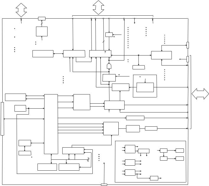
● VIDEO CONTROL UNIT (X14-939x-xx)
Ref.No. |
Application/Function |
Operation/Condition/Compatibility |
|
|
|
IC100 |
SW power supply control IC |
SW5V, mechanism 7V DC/DC |
|
|
|
IC101 |
SW power supply control IC |
SW3.3V, storage mechanism 7.5V DC/DC |
|
|
|
IC102 |
SW power supply control IC |
±7.5V, BL8.5V DC/DC |
|
|
|
IC103 |
3 terminal regulator |
BU5V output |
|
|
|
IC104 |
Low-loss regulator |
BU3.3V output |
|
|
|
IC105 |
2ch comparator |
BU low voltage detection |
|
|
|
IC106 |
Inverter |
P_ON control |
|
|
|
IC107 |
3 terminal regulator drive |
Video system 7.5V output |
|
|
|
IC108 |
Low-loss regulator |
SW2V output |
|
|
|
IC200 |
E2PROM |
System -com memory |
|
|
|
IC202 |
Motor driver |
Slide mechanism motor control |
|
|
|
IC203 |
Motor driver |
Tilt mechanism motor control |
|
|
|
IC204 |
Microcomputer |
System control |
|
|
|
5
DDX7015/7025/7035
DDX7045/7065
COMPONENTS DESCRIPTION
Ref.No. |
Application/Function |
Operation/Condition/Compatibility |
|
|
|
IC205 |
AND |
Remote control output buffer |
|
|
|
IC206 |
Inverter |
Microcomputer reset control |
|
|
|
IC207 |
Reset |
System µ-com reset control at low voltage |
|
|
|
IC300 |
3 terminal regulator |
Video system 5V power supply output |
|
|
|
IC301 |
1H delay |
PAL color difference signal delay |
|
|
|
IC302 |
RGB switch |
RGB signal SYNC cutting |
|
|
|
IC303 |
RGB decoder |
RGB decode |
|
|
|
IC304 |
RGB switch |
DVD/NAVI, TV switching |
|
|
|
IC305 |
3 terminal regulator |
Video system 3V power supply output |
|
|
|
IC306 |
Inverter |
V. MUTE control |
|
|
|
IC361 |
NAND |
HD, VD mix |
|
|
|
IC362 |
Synchronous separation |
Synchronous separation |
|
|
|
IC363,364 |
3ch buffer |
HD, VD buffer |
|
|
|
IC365 |
Mono-multi |
HD timing for OSD |
|
|
|
IC400 |
OSD |
OSD graphic signal occurrence |
|
|
|
IC401 |
Flash ROM |
OSD font data ROM |
|
|
|
IC520 |
Flash ROM |
MPEG decoder control program ROM |
|
|
|
IC521 |
SRAM |
Backup ROM for MPEG decoder |
|
|
|
IC522 |
NAND |
SRAM chip selection |
|
|
|
IC540 |
Inverter |
27MHz buffer |
|
|
|
IC541 |
Inverter |
27MHz oscillation |
|
|
|
IC560 |
SDRAM |
RAM for temporary storage of decoded signal |
|
|
|
IC580 |
ANDx4 (4 AND’s included) |
3.3V→ 5V conversion |
|
|
|
IC601 |
MPEG decoder |
IC for decoding encoded signal |
|
|
|
IC650 |
Driver IC for visual signals |
Lowpass filter + 6dB_AMP + DRIVER |
|
|
|
IC651 |
Regulator IC |
Video 5V regulator |
|
|
|
IC652 |
Video encoder |
Converts digital video signals into analog |
|
|
|
IC701 |
Ope amp |
Active filter circuit for audio signals |
|
|
|
IC702 |
Regulator IC |
Audio 5V regulator |
|
|
|
IC703 |
Audio DAC |
Converts digital audio signals to analog |
|
|
|
IC750 |
Inverter |
Drive for optical output |
|
|
|
IC770 |
CPLD |
Audio DAC control, Chip selection control of SRAM |
|
|
|
Q100~103 |
Digital transistor |
P_ON control |
|
|
|
Q104,105 |
Small signal NPN transistor |
BU reduced current detection |
|
|
|
Q106 |
High-speed power SW FET |
SW14V output |
|
|
|
Q107 |
Small signal NPN transistor |
ACC detection control |
|
|
|
Q108 |
Digital transistor |
Parking detection control |
|
|
|
Q109 |
High-speed power SW FET |
SW5V, mechanism 7V DC/DC |
|
|
|
Q110 |
High-speed power SW FET |
SW3.3V, storage mechanism 7.5V DC/DC |
|
|
|
Q111 |
High-speed power SW FET |
±7.5V, mechanism 7V DC/DC |
|
|
|
6
DDX7015/7025/7035
DDX7045/7065
COMPONENTS DESCRIPTION
Ref.No. |
Application/Function |
Operation/Condition/Compatibility |
|
|
|
|
|
Q112 |
Low-frequency power |
Video system 7.5V output |
|
amplifying PNP transistor |
|||
|
|
||
|
|
|
|
Q113 |
Small signal PNP transistor |
Fan power supply 12.8V output |
|
|
|
|
|
Q114 |
Small signal NPN transistor |
Fan power supply 12.8V output |
|
|
|
|
|
Q115 |
Medium power amplifying |
Fan power supply 12.8V output |
|
PNP transistor |
|||
|
|
||
|
|
|
|
Q116 |
Small signal NPN transistor |
Fan power supply 12.8V output |
|
|
|
|
|
Q117 |
NPN digital transistor |
Storage mechanism power supply switching control |
|
|
|
|
|
Q118 |
Small signal PNP transistor |
BL8.5V over current detection |
|
|
|
|
|
Q119 |
NPN digital transistor |
BL8.5V over current detection |
|
|
|
|
|
Q120 |
Small signal PNP transistor |
BU5V/SW5V switching |
|
|
|
|
|
Q121 |
NPN digital transistor |
BU5V/SW5V switching |
|
|
|
|
|
Q122 |
Small signal PNP transistor |
BU5V/SW5V switching |
|
|
|
|
|
Q123,124 |
Small signal NPN transistor |
BU5V/SW5V switching |
|
|
|
|
|
Q170,171 |
Digital transistor |
SW5V, mechanism 7V DC/DC oscillation frequency switching |
|
|
|
|
|
Q172,173 |
Digital transistor |
SW3.3V, storage mechanism 7.5V DC/DC oscillation frequency switching |
|
|
|
|
|
Q174,175 |
Digital transistor |
±7.5V, mechanism 7V DC/DC oscillation frequency switching |
|
|
|
|
|
Q200,201 |
Digital transistor |
Blue illumination control |
|
|
|
|
|
Q202,203 |
Digital transistor |
Green illumination control |
|
|
|
|
|
Q204,205 |
Digital transistor |
Red illumination control |
|
|
|
|
|
Q206 |
Digital transistor |
BOX microcomputer |
|
|
|
|
|
Q207 |
Digital transistor |
Microcomputer reset control |
|
|
|
|
|
Q300 |
Small signal PNP transistor |
Chroma LPF fc NT/PAL switching |
|
|
|
|
|
Q360 |
Small signal NPN transistor |
Y signal input buffer |
|
|
|
|
|
Q361 |
Small signal PNP transistor |
C signal input buffer |
|
|
|
|
|
Q362 |
Small signal PNP transistor |
Synchronous separation circuit V signal input buffer |
|
|
|
|
|
Q400 |
Small signal PNP transistor |
OSD R signal output buffer |
|
|
|
|
|
Q401 |
Small signal PNP transistor |
OSD G signal output buffer |
|
|
|
|
|
Q402 |
Small signal PNP transistor |
OSD B signal output buffer |
|
|
|
|
|
Q403 |
NPN digital transistor |
OSD clock NT/PAL switching control |
|
|
|
|
|
Q650 |
PNP digital transistor |
RGB_SW reversal |
|
|
|
|
|
Q652 |
NPN digital transistor |
IC650 6pin input signal muting |
|
|
|
|
|
Q701 |
Small signal NPN transistor |
Audio DMIX_L signal muting |
|
|
|
|
|
Q702 |
Small signal NPN transistor |
Audio DMIX_R signal muting |
|
|
|
|
|
Q703 |
Small signal NPN transistor |
Audio mute control |
|
|
|
|
|
Q704~707 |
Digital transistor |
Audio mute control |
|
|
|
|
|
Q751 |
Small signal NPN transistor |
COAX output driving |
|
|
|
|
|
Q752 |
Small signal PNP transistor |
COAX output driving |
|
|
|
|
|
Q901 |
Medium power amplifying |
TDF panel section power supply ON/OFF control |
|
PNP transistor |
|||
|
|
||
|
|
|
|
Q902 |
Small signal NPN transistor |
TDF panel section power supply ON/OFF control |
|
|
|
|
7
DDX7015/7025/7035
DDX7045/7065
COMPONENTS DESCRIPTION
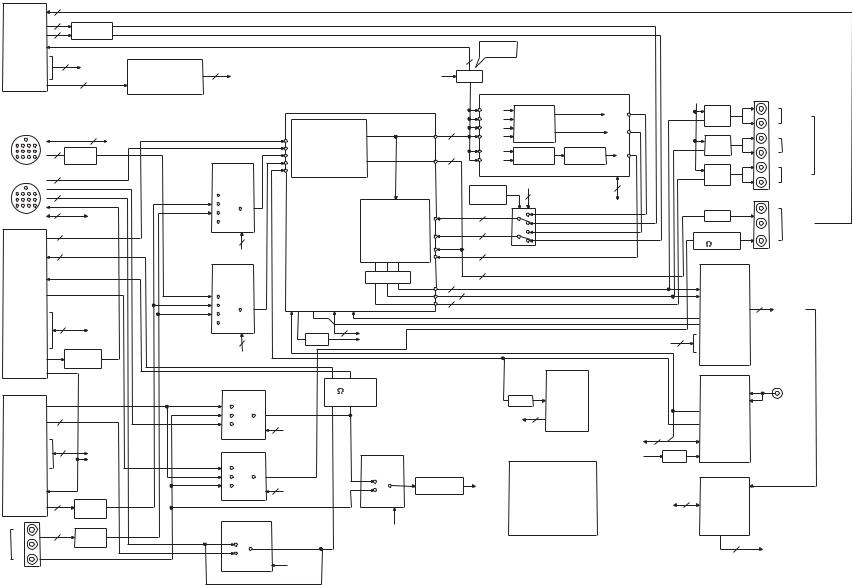
● ELECTRIC UNIT (X34-316x-xx)
Ref.No. |
Application/Function |
Operation/Condition/Compatibility |
|
|
|
|
|
IC1 |
3-terminal regulator IC |
Generates 8.4V for audio from BU14V. |
|
|
|
|
|
IC3 |
3-terminal regulator IC |
Generates 5.0V for visuals from BU14V. |
|
|
|
|
|
IC100 |
Logic IC |
For audio mute control. |
|
|
|
|
|
IC101 |
Logic IC |
When BU5V goes below 3.7V, reset with output L (When microcomputer is flushed, 4.2V). |
|
|
|
|
|
IC103 |
X34 board controller |
Control of X34 board, Communication with other boards and connected devices. |
|
microcomputer |
|||
|
|
||
|
|
|
|
IC200 |
RDS demodulator IC |
Demodulation of RDS signals. |
|
|
|
|
|
IC250 |
Power IC |
Power amplifier for speaker output. |
|
|
|
|
|
IC300 |
Digitally audio processor IC |
4ch hipass filter, 2ch lowpass filter. |
|
|
|
|
|
IC301 |
Electrical volume, Selector, |
|
|
NC MPX IC |
|
||
|
|
||
|
|
|
|
IC350 |
Isolation amplifier IC |
For LX BUS |
|
|
|
|
|
IC400 |
Logic IC |
For making navigation and other remote control lines independent. |
|
|
|
|
|
IC450,451 |
75Ω driver, 6dB amplifier IC |
For video signals from X34 to X14. |
|
|
|
|
|
IC452 |
Logic IC |
For reversing reset signal. |
|
|
|
|
|
IC500 |
Isolation amplifier IC |
For TV TUNER. |
|
|
|
|
|
IC501 |
RGB switch IC |
For selection of RGB signals for TV or NAVI. |
|
|
|
|
|
IC550,554 |
4ch multiplexer |
For selection of audio signals for LX, NAVI, TV or AVIN. |
|
|
|
|
|
IC551 |
Video switch |
For selection of composite signals for IC553 or AVIN. Used for detecting NTSC, PAL and |
|
detecting rear camera. |
|||
|
|
||
|
|
|
|
IC552 |
Sync separator IC |
For determination of NTSC, PAL. |
|
|
|
|
|
IC553 |
75Ω driver + video switch |
For detection of visual output signal for X14 (TV/AVIN/NAVI). |
|
|
|
|
|
IC555 |
75Ω driver + video switch |
For selection of visual output signal for AVOUT (DVD/TV/AVIN). |
|
|
|
|
|
IC600 |
Isolation amplifier IC |
For AVIN. |
|
|
|
|
|
IC700,701 |
Switching ope amplifier |
For isolation of audio signal from DSP box and SW for X34 audio signal. |
|
|
|
|
|
IC702 |
Operational amplifier |
For 1/2VCC supply to BA3121F (LX/TV/AVIN). |
|
|
|
|
|
IC703,704 |
Operational amplifier |
For isolation of audio signal from DSP box. |
|
|
|
|
|
IC900 |
Operational amplifier |
For noise canceling circuit. |
|
|
|
|
|
Q1,2 |
BU5V switch |
Turned ON when BU14V is supplied. |
|
|
|
|
|
Q3 |
BU5V switch |
Turned ON when Q9 is turned ON. |
|
|
|
|
|
Q4 |
A9V switch |
Turned ON when SW14V is supplied. |
|
|
|
|
|
Q5 |
V5V switch |
Turned ON when SW14V is supplied. |
|
|
|
|
|
Q6 |
A9V power supply |
Turned ON when Q4 is turned ON. |
|
|
|
|
|
Q8 |
SW14V switch |
Turned ON when P-ON. |
|
|
|
|
|
Q9 |
SW5V switch |
Turned ON when P-ON. |
|
|
|
|
|
Q10 |
V5V power supply |
Turned ON when Q5 is turned ON. |
|
|
|
|
|
Q19 |
Illumination switch |
Turned ON when illumination is turned ON. |
|
|
|
|
|
Q20 |
ANT-CONT switch |
Turned ON when TUNER is selected. |
|
|
|
|
|
Q21 |
P-CONT |
Turned ON when P-CONT is turned ON. |
|
|
|
|
8
DDX7015/7025/7035
DDX7045/7065
COMPONENTS DESCRIPTION
Ref.No. |
Application/Function |
Operation/Condition/Compatibility |
|
|
|
|
|
Q22 |
P-CONT |
Turned ON when Q21 is turned ON. |
|
|
|
|
|
Q23 |
P-ANT switch |
Turned ON when Q20 is turned ON. |
|
|
|
|
|
Q24 |
P-CONT |
Turned ON when Q25 is turned ON. |
|
|
|
|
|
Q25 |
P-CONT |
Turned ON when BU14V is supplied. Turned OFF when Q22 is turned ON. |
|
|
|
|
|
Q26 |
BU detection switch |
Turned ON when BU is detected. |
|
|
|
|
|
Q27 |
EXT-AMP switch |
Turned ON when EXT-CONT terminal is L. |
|
|
|
|
|
Q100 |
S-MUTE reverse switch |
Turned ON when momentary power down, when reset, and when S-MUTE is turned ON. |
|
|
|
|
|
Q200 |
AM power supply switch |
Turned ON when TUNER is selected. |
|
|
|
|
|
Q201 |
AM power supply switch |
Turned ON when Q200 is turned ON. |
|
|
|
|
|
Q300 |
NOISE switch |
Turned ON when IC301QUAL terminal is Hi. |
|
|
|
|
|
Q301 |
S-MUTE switch |
Turned ON when Q100 is turned ON. |
|
|
|
|
|
Q460 |
TV resetting reverse switch |
Reverses when reset and outputs Hi. |
|
|
|
|
|
Q551~554 |
Voltage conversion audio |
Outputs by converting 5V→ 8V. |
|
selector switch |
|||
|
|
||
|
|
|
|
Q600,601 |
Muting sub-woofer |
Turned ON when Q607 is turned ON. |
|
|
|
|
|
Q602,604~606 |
Muting pre-out |
Turned ON when Q603 is turned ON. |
|
|
|
|
|
Q603 |
Muting pre-out |
Turned ON when momentary power down, when reset, and when MUTE_PRE is turned ON. |
|
|
|
|
|
Q607 |
Muting sub-woofer |
Turned ON when momentary power down, when reset, and when MUTE_SW is turned ON. |
|
|
|
|
|
Q608,610 |
Muting AVOUT |
Turned ON when Q609 is turned ON. |
|
|
|
|
|
Q609 |
Muting AVOUT |
Turned ON when momentary power down, when reset, and when MUTE_AVOUT is turned ON. |
|
|
|
|
|
Q700 |
IC700, 701 switching switch |
Controlled by ES_DSP_SW. |
|
|
|
|
|
Q702 |
Muting GSM left audio |
Turned ON when momentary power down, when reset, and when MUTE_LEFT is turned ON. |
|
|
|
|
|
Q703 |
Muting GSM left audio |
Q702 is turned ON. |
|
|
|
|
|
Q704 |
FAN5V |
MZ_SYS_ON is turned ON. Turned OFF when MZ_SYS_OFF is turned ON. |
|
|
|
|
|
Q705 |
For J701 |
Turned ON/OFF by 05 signal. |
|
(optical output connector) |
|||
|
|
||
|
|
|
|
Q706 |
Muting GSM right audio |
Turned ON when Q707 is turned ON. |
|
|
|
|
|
Q707 |
Muting GSM right audio |
Turned ON when momentary power down, when reset, and when MUTE_RIGHT is turned ON. |
|
|
|
|
|
Q712 |
Muting BUS |
Turned ON when BUS_MUTE is turned ON. |
|
|
|
|
|
Q713 |
Muting BUS |
Turned ON when Q712 is turned ON. |
|
|
|
|
|
Q904~906 |
Noise canceller |
- |
|
|
|
|
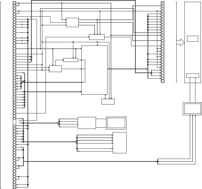
● VIDEO UNIT (X35-4332-70)
Ref.No. |
Application/Function |
Operation/Condition/Compatibility |
|
|
|
IC1 |
Inverter control IC |
Controlling and driving inverter circuit for backlight. |
|
|
|
IC101 |
DC/DC converter |
±12V power supply for VCOM amplifier, -12.0V/+18.5V LCD power supply. |
|
|
|
IC203 |
VCOM amplifier |
VCOM signal amplifier. |
|
|
|
IC301 |
Timing controller |
LCD module control. |
|
|
|
IC302 |
AND |
V. SYNC delay buffer. |
|
|
|
IC303 |
PLL LPF |
PLL control LPF (VT voltage control). |
|
|
|
9
DDX7015/7025/7035
DDX7045/7065
COMPONENTS DESCRIPTION
Ref.No. |
Application/Function |
Operation/Condition/Compatibility |
|
|
|
IC304 |
Schmidt inverter |
CLAMP/C. SYNC waveform shaping. |
|
|
|
IC601 |
Remote controller sensor |
Remote controller sensor. |
|
|
|
Q1 |
Dimmer switch |
Turned ON/OFF by PWM control signal and dimmer is put on the backlight. |
|
|
|
Q2,3 |
Inverter driver |
Inverter circuit driver. |
|
|
|
Q5 |
5V AVR |
5V power supply for inverter control IC. |
|
|
|
Q101,102 |
SW |
DC/DC converter control switch. |
|
|
|
Q201~203 |
VCOM driver |
VCOM signal buffer. |
|
|
|
Q301 |
VCO |
PLL oscillator. |
|
|
|
Q302 |
Touch panel X1 switch |
Turned ON when a touch to the panel is detected, or when input on X-axis and impresses voltage. |
|
|
|
Q303 |
Touch panel Y1 switch |
Turned ON when there is input on Y-axis and impresses voltage. |
|
|
|
Q304 |
Touch panel X0 switch |
Turned ON when there is input on X-axis and impresses voltage. |
|
|
|
Q305 |
Touch panel Y0 switch |
Turned ON when there is input on Y-axis and impresses voltage. |
|
|
|
Q306 |
Touch panel Y0/Y1 switch |
Turned ON when there is input on Y-axis and turned OFF when there is input on X-axis. |
|
|
|
Q601,602 |
Switch |
SI blinking switch. |
|
|
|
Q604,605 |
Switch |
Hard resetting switch. |
|
|
|
Q701 |
Switch |
DISC slot illumination switch. |
|
|
|
MICROCOMPUTER’S TERMINAL DESCRIPTION
● SYSTEM MICROCOMPUTER : 703068YGJ-108 (X14 : IC204)
Pin No. |
Pin Name |
I/O |
Module |
Function |
Processing Operation Description |
|
|
|
|
|
|
1 |
AUTO_DIM |
|
|
NC |
|
|
|
|
|
|
|
2 |
KEY4 |
I |
KEY |
Keys (5) |
|
|
|
|
|
|
|
3 |
KEY3 |
I |
KEY |
Keys (6) |
|
|
|
|
|
|
|
4 |
NC |
I |
|
|
|
|
|
|
|
|
|
5 |
PORTGND0 |
- |
COM |
|
|
|
|
|
|
|
|
6 |
PM1_SWD |
|
|
NC |
|
|
|
|
|
|
|
7 |
LCD_VOFF_EN |
O |
LCD |
ON/OFF control over backlight power supply |
H : ON, L : OFF |
|
|
|
|
|
|
8 |
NC |
O |
|
L-fixed |
|
|
|
|
|
|
|
9 |
TP_YG |
O |
Touch Panel |
Touch panel control |
|
|
|
|
|
|
|
10 |
TP_XP |
O |
Touch Panel |
Touch panel control |
|
|
|
|
|
|
|
11 |
TP_XG |
O |
Touch Panel |
Touch panel control |
|
|
|
|
|
|
|
12~15 |
LCD_HPOSI1~LCD_HPOSI4 |
O |
LCD |
Setting display start position |
|
|
|
|
|
|
|
16~18 |
LCD_MODE1~LCD_MODE3 |
O |
LCD |
Setting aspects |
|
|
|
|
|
|
|
19 |
LCD_MIRROR |
O |
LCD |
Screen display right-left reversal |
H : Reverse, L : Normal |
|
|
|
|
|
|
20 |
ILL_R |
O |
LED (ILLUMI) |
Illumination (red) control |
H : Light on |
|
|
|
|
|
|
21 |
ILL_G |
O |
LED (ILLUMI) |
Illumination (green) control |
H : Light on |
|
|
|
|
|
|
10
DDX7015/7025/7035
DDX7045/7065
MICROCOMPUTER’S TERMINAL DESCRIPTION
Pin No. |
Pin Name |
I/O |
Module |
Function |
Processing Operation Description |
|
|
|
|
|
|
|
|
22 |
PORTVDD0 |
- |
COM |
|
|
|
|
|
|
|
|
|
|
23 |
ILL_B |
O |
LED (ILLUMI) |
Sub-panel backlight (blue) control |
H : Light on |
|
|
|
|
|
|
|
|
24 |
NTSC_PAL |
O |
VIDEO |
NTSC/PAL switching |
H : PAL, L : NTSC |
|
|
|
|
|
|
|
|
25 |
PM_LED_SW/PM_LED_SW |
|
|
NC |
|
|
|
|
|
|
|
||
PM_LED_SW/SI |
O |
LED (SI) |
LED control for SI |
H : Light on, L : Light off |
||
|
||||||
|
|
|
|
|
|
|
26 |
LCD_PON |
O |
Power supply |
DC/DC (X35) power supply ON/OFF control |
H : ON |
|
|
|
|
|
|
|
|
27~29 |
NC |
O |
|
L-fixed |
|
|
|
|
|
|
|
|
|
30 |
V_MUTE |
O |
VIDEO |
Video mute |
H : Mute ON |
|
|
|
|
|
|
|
|
31 |
RGB_SW |
O |
VIDEO |
Switching visual sources |
H : DVD, L : Except |
|
|
|
|
|
|
|
|
32 |
S_MUTE |
O |
VIDEO |
C.SYNC mute |
H : Except, L : Full OSD screen |
|
|
|
|
|
|
|
|
33 |
SYS_SREQ |
I |
to X25 |
Request from Box control microcomputer |
|
|
|
|
|
|
|
|
|
34 |
SYS_MREQ |
O |
to X25 |
Request to Box control microcomputer |
|
|
|
|
|
|
|
|
|
35 |
SYS_ON |
O |
to X25 |
ON/OFF control on Box control microcomputer |
H : ON, L : OFF |
|
|
|
|
|
|
|
|
36 |
CLKOUT |
|
|
|
|
|
|
|
|
|
|
|
|
37 |
GND0 |
- |
COM |
|
|
|
|
|
|
|
|
|
|
38 |
CPUREG |
- |
COM |
|
|
|
|
|
|
|
|
|
|
39 |
VDD0 |
- |
COM |
|
|
|
|
|
|
|
|
|
|
40 |
RESET |
|
|
Reset terminal |
L : Reset |
|
|
|
|
|
|
|
|
41 |
FROM_VPP |
- |
COM |
|
|
|
|
|
|
|
|
|
|
42 |
MINI_CS |
|
|
NC |
|
|
|
|
|
|
|
||
FLASH_SI |
I |
V850 |
Used when writing to flash memory |
|
||
|
|
|||||
|
|
|
|
|
|
|
|
MINI_DATA/MINI_DATA |
|
|
NC |
|
|
|
|
|
|
|
|
|
43 |
MINI_DATA/LEDSW_SUB |
|
|
NC |
|
|
|
|
|
|
|
|
|
|
MINI_DATA/FLASH_SO |
O |
V850 |
Used when writing to flash memory |
|
|
|
|
|
|
|
|
|
44 |
MINI_CLK/MINI_CLK |
|
|
NC |
|
|
|
|
|
|
|
||
MINI_CLK/FLASH_CLK |
I |
V850 |
Used when writing to flash memory |
|
||
|
|
|||||
|
|
|
|
|
|
|
45 |
KEY_OPEN |
I |
KEY |
OPEN/CLOSE key |
L : Key depressed |
|
|
|
|
|
|
|
|
46 |
BE_SDATA |
I |
FR30 |
Data from B/E microcomputer |
|
|
|
|
|
|
|
|
|
47 |
BE_MDATA |
O |
FR30 |
Data to B/E microcomputer |
|
|
|
|
|
|
|
|
|
48 |
BE_CLK |
O |
FR30 |
Clock to B/E microcomputer |
|
|
|
|
|
|
|
|
|
49 |
BE_RST |
O |
FR30 |
Reset to B/E microcomputer |
L : Reset |
|
|
|
|
|
|
|
|
50 |
BE_MREQ |
O |
FR30 |
Request to B/E microcomputer |
|
|
|
|
|
|
|
|
|
51 |
BE_SREQ |
I |
FR30 |
Request from B/E microcomputer |
|
|
|
|
|
|
|
|
|
52 |
PON |
O |
Power supply (X14) |
Power supply ON/OFF control |
H : ON |
|
|
|
|
|
|
|
|
53 |
PM1_MCNT |
O |
1DIN Mecha |
7.5V power supply voltage control |
H : 5V, L : 7.5V |
|
|
|
|
|
|
|
|
54 |
POWER_DET |
I |
Power supply (X14) |
Power supply abnormality detection |
L : Abnormality |
|
|
|
|
|
|
|
|
55 |
PAK_DET |
I |
DC Cable (X14) |
Parking detection |
H : Parking detection |
|
(When car stopped) |
||||||
|
|
|
|
|
||
|
|
|
|
|
|
|
56 |
M_MUTE |
O |
|
Audio mute control |
L : Mute ON |
|
|
|
|
|
|
|
|
57 |
DVD_DISC_DET |
I |
DVS-3000 |
Disc insertion detection |
L : Disc insertion |
|
|
|
|
|
|
|
|
58 |
NC |
O |
|
L-fixed |
|
|
|
|
|
|
|
|
11
DDX7015/7025/7035
DDX7045/7065
MICROCOMPUTER’S TERMINAL DESCRIPTION
Pin No. |
Pin Name |
I/O |
Module |
Function |
Processing Operation Description |
|
|
|
|
|
|
|
|
59 |
D_MUTE |
|
|
NC |
|
|
|
|
|
|
|
|
|
60 |
PORTVDD1 |
- |
COM |
|
|
|
|
|
|
|
|
|
|
61 |
LCD_BRIGHT |
O |
LCD |
Backlight adjustment |
|
|
|
|
|
|
|
|
|
62~65 |
NC |
O |
|
L-fixed |
|
|
|
|
|
|
|
|
|
66 |
JIG_EJ |
I |
EXTRA |
2DIN FC detection terminal |
H : At FC, L : Except |
|
|
|
|
|
|
|
|
67 |
NC |
O |
|
L-fixed |
|
|
|
|
|
|
|
|
|
68 |
SUBLED_OFF |
O |
to PANEL |
Sub panel LED ON/OFF |
Depends on tilt angle |
|
(H : At eject, L : except) |
||||||
|
|
|
|
|
||
|
|
|
|
|
|
|
69 |
ACC_DET |
I |
DC Cable (X14) |
ACC detection |
L : ACC ON |
|
|
|
|
|
|
|
|
70 |
XT2 |
- |
COM |
|
|
|
|
|
|
|
|
|
|
71 |
XT1 |
|
|
|
|
|
|
|
|
|
|
|
|
72 |
GND2 |
- |
COM |
|
|
|
|
|
|
|
|
|
|
73 |
X1 |
|
|
19.8MHz |
|
|
|
|
|
|
|
|
|
74 |
X2 |
- |
COM |
|
|
|
|
|
|
|
|
|
|
75~78 |
NC |
O |
|
L-fixed |
|
|
|
|
|
|
|
|
|
79,80 |
FSEL1, FSEL2 |
O |
Power supply |
DC/DC oscillation frequency switching |
|
|
|
|
|
|
|
|
|
81 |
BU_DET |
I |
DC Cable (X14) |
Backup power down detection |
H : Momentary power down |
|
|
|
|
|
|
|
|
82 |
KEY_SRC |
I |
KEY |
Source selection key |
L : Key depressed |
|
|
|
|
|
|
|
|
83 |
KEY_DVDEJ |
I |
KEY |
DVD eject key |
L : Key depressed |
|
|
|
|
|
|
|
|
|
SDA/CHROMA_SDA |
I/O |
CHROMA |
Chroma IC data |
AN2546 control |
|
|
|
|
|
|
|
|
|
CODE_SDA |
I/O |
EEPROM (CODE) |
EEPROM (Code) data |
S-24CS02 control |
|
|
|
|
|
|
|
|
|
SDA/BE_SDA |
I/O |
EEPROM (DVD) |
EEPROM (Region) data |
S-24CS02 control |
|
|
|
|
|
|
|
|
84 |
SDA/LCD_SDA |
I/O |
EEPROM (LCD) |
EEPROM (Display start position) data |
S-24CS02 control |
|
|
|
|
|
|
|
|
|
SDA/COR_SDA |
I/O |
EEPROM (ROM collection) |
EEPROM (ROM collection) data |
S-24CS02 control |
|
|
|
|
|
|
|
|
|
SDA/TP_SDA |
I/O |
EEPROM (TP) |
EEPROM (Adjustment value) data |
S-24CS02 control |
|
|
|
|
|
|
|
|
|
SDA/CADJ_SDA |
I/O |
|
E2PROM chroma IC adjustment value data |
S-24CS02 control |
|
|
|
|
|
|
|
|
85 |
NC |
O |
|
L-fixed |
|
|
|
|
|
|
|
|
|
|
SCL/CHROMA_SCL |
I/O |
CHROMA |
Chroma IC clock |
|
|
|
|
|
|
|
|
|
|
CODE_SCL |
I/O |
EEPROM (CODE) |
EEPROM (Code) clock |
S-24CS02 control |
|
|
|
|
|
|
|
|
|
SCL/BE_SCL |
I/O |
EEPROM (DVD) |
EEPROM (Region) clock |
S-24CS02 control |
|
|
|
|
|
|
|
|
86 |
SCL/LCD_SCL |
I/O |
EEPROM (LCD) |
EEPROM (Display start position) clock |
S-24CS02 control |
|
|
|
|
|
|
|
|
|
SCL/COR_SCL |
I/O |
EEPROM (ROM collection) |
EEPROM (ROM collection) clock |
S-24CS02 control |
|
|
|
|
|
|
|
|
|
SCL/TP_SCL |
I/O |
EEPROM (TP) |
EEPROM (Adjustment value) clock |
S-24CS02 control |
|
|
|
|
|
|
|
|
|
SCL/CADJ_SCL |
I/O |
|
E2PROM chroma IC adjustment value data |
AN2546 control |
|
|
|
|
|
|
|
|
87~91 |
NC |
O |
|
L-fixed |
|
|
|
|
|
|
|
|
|
92 |
PORTGND1 |
- |
COM |
|
|
|
|
|
|
|
|
|
|
93 |
MINI_CLK_IN |
|
|
NC |
|
|
|
|
|
|
|
|
|
94 |
MINI_DATA_IN |
|
|
NC |
|
|
|
|
|
|
|
|
|
95 |
NC |
O |
|
L-fixed |
|
|
|
|
|
|
|
|
|
96 |
PAN_DET |
|
|
NC |
|
|
|
|
|
|
|
|
|
97 |
OSD_CLK |
O |
LC74735W |
Clock to OSDC-IC |
|
|
|
|
|
|
|
|
12
DDX7015/7025/7035
DDX7045/7065
MICROCOMPUTER’S TERMINAL DESCRIPTION
Pin No. |
Pin Name |
I/O |
Module |
Function |
Processing Operation Description |
|
|
|
|
|
|
|
|
98 |
OSD_CS |
O |
LC74735W |
Chip select to OSDC-IC |
|
|
|
|
|
|
|
|
|
99 |
OSD_DATA |
O |
LC74735W |
Data to OSDC-IC |
|
|
|
|
|
|
|
|
|
100 |
NC |
O |
|
L-fixed |
|
|
|
|
|
|
|
|
|
101 |
DSI |
|
|
NC |
|
|
|
|
|
|
|
|
|
102 |
PORTVDD2 |
- |
COM |
|
|
|
|
|
|
|
|
|
|
103 |
MINI_PON |
|
|
NC |
|
|
|
|
|
|
|
|
|
104 |
PM1_SET_STATUS0 |
|
|
NC |
|
|
|
|
|
|
|
|
|
105 |
PM1_SET_STATUS1 |
|
|
NC |
|
|
|
|
|
|
|
|
|
106 |
PM1_SET_STATUS2 |
|
|
NC |
|
|
|
|
|
|
|
|
|
107 |
SYS_SDATA |
I |
to X25 |
Data from Box control microcomputer |
|
|
|
|
|
|
|
|
|
108 |
SYS_MDATA |
O |
to X25 |
Data to Box control microcomputer |
|
|
|
|
|
|
|
|
|
109 |
SYS_MCLK |
O |
to X25 |
Clock to Box control microcomputer |
|
|
|
|
|
|
|
|
|
110 |
NC |
O |
|
L-fixed |
|
|
|
|
|
|
|
|
|
111 |
WRT_E2P |
I |
EXTRA |
Write detection at ROM collection |
H : E2PROM writing |
|
from outside, L : Except |
||||||
|
|
|
|
|
||
|
|
|
|
|
|
|
112~115 |
TYPE0~TYPE3 |
I |
Type |
Destination setting |
|
|
|
|
|
|
|
|
|
116~119 |
NC |
O |
|
L-fixed |
|
|
|
|
|
|
|
|
|
120 |
OSD_RST |
O |
LC74735W |
Reset to OSDC-IC |
L : Reset |
|
|
|
|
|
|
|
|
121 |
OSD_A18 |
I/O |
LC74735W |
External ROM address bus A18 |
3.3V |
|
|
|
|
|
|
|
|
122 |
OSD_A19 |
I/O |
LC74735W |
External ROM address bus A19 |
3.3V |
|
|
|
|
|
|
|
|
123 |
NC |
O |
|
L-fixed |
|
|
|
|
|
|
|
|
|
124 |
PM1_TMOTOR_M |
|
|
NC |
|
|
|
|
|
|
|
||
PM2_TILT_UP |
O |
2DIN Mecha |
Panel mechanism motor control |
|
||
|
|
|||||
|
|
|
|
|
|
|
125 |
VD |
I |
VIDEO |
Old-New NAVI determination VSYNC |
|
|
|
|
|
|
|
|
|
126 |
PM1_TMOTOR_P |
|
|
NC |
|
|
|
|
|
|
|
||
PM2_TILT_DOWN |
O |
2DIN Mecha |
Panel mechanism motor control |
|
||
|
|
|||||
|
|
|
|
|
|
|
127 |
PM1_SMOTOR_M |
|
|
NC |
|
|
|
|
|
|
|
|
|
128 |
VDD1 |
- |
COM |
|
|
|
|
|
|
|
|
|
|
129 |
PM1_SMOTOR_P |
|
|
NC |
|
|
|
|
|
|
|
|
|
130 |
PM1_SWC |
|
|
NC |
|
|
|
|
|
|
|
|
|
131 |
GND1 |
- |
COM |
|
|
|
|
|
|
|
|
|
|
132 |
PM1_SWB |
|
|
NC |
|
|
|
|
|
|
|
|
|
133 |
PM1_SWA |
|
|
NC |
|
|
|
|
|
|
|
|
|
134 |
NC |
O |
|
L-fixed |
|
|
|
|
|
|
|
|
|
135 |
KEY2 |
|
|
NC |
|
|
|
|
|
|
|
|
|
136 |
VOL- |
|
|
NC |
|
|
|
|
|
|
|
|
|
137 |
VOL+ |
|
|
NC |
|
|
|
|
|
|
|
|
|
138 |
PM_LPS/PM1_LPS1 |
I |
1DIN Mecha |
TV mechanism tilt sensor voltage detection |
|
|
|
|
|
|
|
||
PM_LPS/PM2_TILT_SENCE |
I |
2DIN Mecha |
Panel mechanism tilt sensor voltage detection |
|
||
|
|
|||||
|
|
|
|
|
|
|
139 |
PM1_PHOTO1 |
I |
1DIN Mecha |
TV mechanism slide photo detection |
|
|
|
|
|
|
|
|
|
140 |
TP_YDATA |
I |
Touch Panel |
Touch panel input (Y-direction) |
|
|
|
|
|
|
|
|
13
DDX7015/7025/7035
DDX7045/7065
MICROCOMPUTER’S TERMINAL DESCRIPTION
Pin No. |
Pin Name |
I/O |
Module |
Function |
Processing Operation Description |
|
|
|
|
|
|
141 |
TP_XDATA |
I |
Touch Panel |
Touch panel input (X-direction) |
|
|
|
|
|
|
|
142 |
KEY1 |
|
|
NC |
|
|
|
|
|
|
|
143 |
ADCVDD |
- |
COM |
|
|
|
|
|
|
|
|
144 |
ADCGND |
- |
COM |
|
|
|
|
|
|
|
|
Destination Setting
Model |
Destination |
TYPE3 |
TYPE2 |
TYPE1 |
TYPE0 |
|
|
|
|
|
|
KVT-715DVD |
K |
0 |
0 |
0 |
1 |
|
|
|
|
|
|
KVT-725DVD |
E |
0 |
0 |
1 |
0 |
|
|
|
|
|
|
KVT-735DVD |
M |
0 |
0 |
1 |
1 |
|
|
|
|
|
|
KVT-765/745DVD |
C,X |
0 |
1 |
0 |
0 |
|
|
|
|
|
|
KVT-815DVD |
K2 eXcelon |
0 |
1 |
1 |
0 |
|
|
|
|
|
|
KVT-745DVD |
R |
0 |
1 |
1 |
1 |
|
|
|
|
|
|
DDX7015 |
K |
1 |
0 |
0 |
1 |
|
|
|
|
|
|
DDX7025 |
E |
1 |
0 |
1 |
0 |
|
|
|
|
|
|
DDX7035 |
M |
1 |
0 |
1 |
1 |
|
|
|
|
|
|
DDX7065/7045 |
C,X |
1 |
1 |
0 |
0 |
|
|
|
|
|
|
DDX7045 |
R |
1 |
1 |
1 |
1 |
|
|
|
|
|
|
● TUNER MICROCOMPUTER : 703069YGJ-104 (X34 : IC103)
Pin No. |
Pin Name |
Module |
I/O |
Application |
Processing Operation |
Active |
Truth |
|
Description |
(H/L) |
Value |
||||||
|
|
|
|
|
||||
|
|
|
|
|
|
|
|
|
1 |
NC |
|
I |
|
Pull down |
|
|
|
|
|
|
|
|
|
|
|
|
2 |
RDS_NOISE |
IC2-5-2 |
I |
FM noise detection |
|
|
|
|
|
|
|
|
|
|
|
|
|
3 |
DC_ERR |
IC2-5-2 |
I |
DC offset detection |
L when detected |
|
|
|
|
|
|
|
|
|
|
|
|
4 |
LINE_MUTE |
DC Cable (X25) |
I |
LINE MUTE detection |
TEL mute : 1V or lower, |
|
|
|
NAVI mute : 2.5V or higher |
|
|
||||||
|
|
|
|
|
|
|
||
|
|
|
|
|
|
|
|
|
5 |
PORTGND0 |
COM |
- |
|
|
|
|
|
|
|
|
|
|
|
|
|
|
6 |
AUDIO_SW1_B |
Visual |
O |
LX/TV/AVIN audio switching |
|
|
r |
|
|
|
|
|
|
|
|
|
|
7 |
MUTE_PRE |
Mute |
O |
PREOUT mute |
L : Mute ON |
L |
|
|
|
|
|
|
|
|
|
|
|
8 |
AUDIO_SW2_A |
Visual |
O |
LX/TV/AVIN audio switching |
|
|
r |
|
|
|
|
|
|
|
|
|
|
9 |
AUDIO_SW2_B |
Visual |
O |
LX/TV/AVIN audio switching |
|
|
r |
|
|
|
|
|
|
|
|
|
|
10 |
AUD_SCL |
IC2-5-2 |
I/O |
IC2-5-2 clock |
Based on IIC bus regulation |
|
|
|
|
|
|
|
|
|
|
|
|
11 |
AUD_SDA |
IC2-5-2 |
I/O |
IC2-5-2 data |
Based on IIC bus regulation |
|
|
|
|
|
|
|
|
|
|
|
|
12 |
S_MUTE |
IC2-5-2 |
O |
S-MUTE control |
H : Mute ON, L : Mute OFF |
H |
|
|
|
|
|
|
|
|
|
|
|
13 |
AUDIO_SW1_A |
Visual |
O |
LX/TV/AVIN audio switching |
|
|
r |
|
|
|
|
|
|
|
|
|
|
14 |
RDS_AFS_L |
IC2-5-2 |
I/O |
When detecting noise, constant is switched |
|
|
q |
|
|
|
|
|
|
|
|
|
|
15 |
RDS_AFS_M |
IC2-5-2 |
I/O |
When detecting noise, constant is switched |
|
|
q |
|
|
|
|
|
|
|
|
|
|
16 |
MUTE_LEFT |
Mute |
O |
Lch independent muting for handsfree |
L : Mute ON |
L |
|
|
|
|
|
|
|
|
|
|
|
17 |
MUTE_RIGHT |
Mute |
O |
Rch independent muting for handsfree |
L : Mute ON |
L |
|
|
|
|
|
|
|
|
|
|
14
DDX7015/7025/7035
DDX7045/7065
MICROCOMPUTER’S TERMINAL DESCRIPTION
Pin No. |
Pin Name |
Module |
I/O |
Application |
Processing Operation |
Active |
Truth |
|
Description |
(H/L) |
Value |
||||||
|
|
|
|
|
||||
|
|
|
|
|
|
|
|
|
18 |
VISUAL_SW1_1 |
Visual |
O |
TV/AVIN/NAVI visual switching |
|
|
t |
|
|
|
|
|
|
|
|
|
|
19 |
VISUAL_SW1_2 |
Visual |
O |
TV/AVIN/NAVI visual switching |
|
|
t |
|
|
|
|
|
|
|
|
|
|
20 |
VISUAL_SW2_1 |
Visual |
O |
DVD/TV/AVIN visual switching |
|
|
t |
|
|
|
|
|
|
|
|
|
|
21 |
VISUAL_SW2_2 |
Visual |
O |
DVD/TV/AVIN visual switching |
|
|
t |
|
|
|
|
|
|
|
|
|
|
22 |
PORTVDD0 |
COM |
- |
|
|
|
|
|
|
|
|
|
|
|
|
|
|
23 |
MUTE_AVOUT |
Mute |
O |
AVOUT mute |
L : Mute ON |
L |
|
|
|
|
|
|
|
|
|
|
|
24 |
NC |
|
O |
|
|
|
|
|
|
|
|
|
|
|
|
|
|
25 |
MUTE_SUBOUT |
Mute |
O |
IC2 SUBOUT mute (land compatible) |
L : Mute ON |
L |
|
|
|
|
|
|
|
|
|
|
|
26 |
NC |
|
O |
|
|
|
|
|
|
|
|
|
|
|
|
|
|
27 |
SYS_MREQ |
to X14 |
I |
Request from system control microcomputer |
|
|
|
|
|
|
|
|
|
|
|
|
|
28 |
SYS_SREQ |
to X14 |
O |
Request to system control microcomputer |
|
|
|
|
|
|
|
|
|
|
|
|
|
29~32 |
NC |
|
O |
|
|
|
|
|
|
|
|
|
|
|
|
|
|
33 |
P_CON |
DC Cable (X25) |
O |
External amplifier power supply control |
H : Power ON except all OFF, |
|
|
|
L : All OFF or Power OFF |
|
|
||||||
|
|
|
|
|
|
|
||
|
|
|
|
|
|
|
|
|
34 |
EXT_CONT |
DC Cable (X25) |
O |
External amplifier control |
|
|
|
|
|
|
|
|
|
|
|
|
|
35 |
ANT_CONT |
DC Cable (X25) |
O |
Power antenna control |
H : Antenna UP, |
|
|
|
L : Antenna DOWN |
|
|
||||||
|
|
|
|
|
|
|
||
|
|
|
|
|
|
|
|
|
36 |
CLKOUT |
|
O |
|
|
|
|
|
|
|
|
|
|
|
|
|
|
37 |
GND0 |
COM |
- |
|
|
|
|
|
|
|
|
|
|
|
|
|
|
38 |
CPUREG |
COM |
- |
|
|
|
|
|
|
|
|
|
|
|
|
|
|
39 |
VDD0 |
COM |
- |
|
|
|
|
|
|
|
|
|
|
|
|
|
|
40 |
RESET |
|
I |
|
|
|
|
|
|
|
|
|
|
|
|
|
|
41 |
MODE/VPP |
COM |
- |
|
Flash : Pull down, |
|
|
|
|
Mask : GND direct connection |
|
|
|||||
|
|
|
|
|
|
|
||
|
|
|
|
|
|
|
|
|
42 |
TV_SDATA/TV_SDATA |
TV (External) |
I |
Data from the TV unit |
|
|
|
|
|
|
|
|
|
|
|
||
TV_SDATA/FLASH_SI |
V850 |
I |
Used when writing to flash memory |
|
|
|
||
|
|
|
|
|||||
|
|
|
|
|
|
|
|
|
43 |
TV_MDATA/TV_MDATA |
TV (External) |
O |
Data to TV unit |
|
|
|
|
|
|
|
|
|
|
|
||
TV_MDATA/FLASH_SO |
V850 |
O |
Used when writing to flash memory |
|
|
|
||
|
|
|
|
|||||
|
|
|
|
|
|
|
|
|
44 |
TV_CLK/TV_CLK |
TV (External) |
O |
Clock to TV unit |
|
|
|
|
|
|
|
|
|
|
|
||
TV_CLK/FLASH_CLK |
V850 |
I |
Used when writing to flash memory |
|
|
|
||
|
|
|
|
|||||
|
|
|
|
|
|
|
|
|
45 |
SYS_ON |
to X14 |
I |
ON/OFF control from system control |
H : Box unit ON, |
|
|
|
microcomputer |
L : Box unit OFF |
|
|
|||||
|
|
|
|
|
|
|||
|
|
|
|
|
|
|
|
|
46 |
SYS_MDATA |
to X14 |
I |
Data from system control microcomputer |
|
|
|
|
|
|
|
|
|
|
|
|
|
47 |
SYS_SDATA |
to X14 |
O |
Data to system control microcomputer |
|
|
|
|
|
|
|
|
|
|
|
|
|
48 |
SYS_MCLK |
to X14 |
I |
Clock from system control microcomputer |
|
|
|
|
|
|
|
|
|
|
|
|
|
49 |
PWIC_STBY |
POWER-IC |
O |
POWER-IC standby control |
H : Power ON, L : Power OFF |
|
|
|
|
|
|
|
|
|
|
|
|
50 |
NC |
|
O |
|
|
|
|
|
|
|
|
|
|
|
|
|
|
51 |
PWIC_SVR |
POWER-IC |
O |
SVR discharge circuit control |
H : Forced discharge |
|
|
|
|
|
|
|
|
|
|
|
|
52 |
PWIC_MUTE |
POWER-IC |
O |
POWER-IC Mute control |
L : Mute ON (All OFF or |
|
|
|
momentary power down) |
|
|
||||||
|
|
|
|
|
|
|
||
|
|
|
|
|
|
|
|
15
DDX7015/7025/7035
DDX7045/7065
MICROCOMPUTER’S TERMINAL DESCRIPTION
Pin No. |
Pin Name |
Module |
I/O |
Application |
Processing Operation |
Active |
Truth |
|
Description |
(H/L) |
Value |
||||||
|
|
|
|
|
||||
|
|
|
|
|
|
|
|
|
53 |
NC |
|
O |
|
|
|
|
|
|
|
|
|
|
|
|
|
|
54 |
ILLUMI_DET |
DC Cable (X25) |
I |
Illumination detection |
L : Illumination ON |
L |
|
|
|
|
|
|
|
|
|
|
|
55,56 |
NC |
|
O |
|
O |
|
|
|
|
|
|
|
|
|
|
|
|
57 |
BU_DET |
DC Cable (X25) |
I |
Backup power down detection |
H : Momentary power |
|
|
|
down (8.8V or lower) |
|
|
||||||
|
|
|
|
|
|
|
||
|
|
|
|
|
|
|
|
|
58,59 |
NC |
|
O |
|
|
|
|
|
|
|
|
|
|
|
|
|
|
60 |
PORTVDD1 |
COM |
- |
|
|
|
|
|
|
|
|
|
|
|
|
|
|
61 |
PWIC_BEEP |
POWER-IC |
O |
Beep output |
|
|
|
|
|
|
|
|
|
|
|
|
|
62 |
P_ON |
power supply |
O |
SW5V power supply control |
H : ON |
|
|
|
|
|
|
|
|
|
|
|
|
|
SCL/COR_SCL |
EEPROM |
I/O |
EEPROM (ROM collection) clock |
Based on IIC bus regulation |
|
|
|
63 |
(ROM collection) |
|
|
|||||
|
|
|
|
|
|
|||
|
|
|
|
|
|
|
|
|
|
SCL/IC5_SCL |
IC5 |
I/O |
IC5 clock |
Based on IIC bus regulation |
|
|
|
|
|
|
|
|
|
|
|
|
|
SDA/COR_SDA |
EEPROM |
I/O |
EEPROM (ROM collection) data |
Based on IIC bus regulation |
|
|
|
64 |
(ROM collection) |
|
|
|||||
|
|
|
|
|
|
|||
|
|
|
|
|
|
|
|
|
|
SDA/IC5_SDA |
IC5 |
I/O |
IC5 data |
Based on IIC bus regulation |
|
|
|
|
|
|
|
|
|
|
|
|
65 |
ES_DSP_SW |
Audio |
O |
E’s/DSP switching |
H : DSP, L : E’s |
|
|
|
|
|
|
|
|
|
|
|
|
66 |
BUS_MUTE |
Mute |
O |
BUS_MUTE |
H : Mute |
H |
|
|
|
|
|
|
|
|
|
|
|
67 |
MZ_ILL_ON |
MZ-Bus |
O |
MZ-Bus ILLUMI control |
H : ILLUMI ON |
H |
|
|
|
|
|
|
|
|
|
|
|
68 |
MZ_SYSON |
MZ-Bus |
O |
MZ-Bus SYSON control |
L : Bus ON |
L |
|
|
|
|
|
|
|
|
|
|
|
69 |
MZ_SYSOFF |
MZ-Bus |
O |
MZ-Bus SYSOFF control |
L : Bus OFF |
L |
|
|
|
|
|
|
|
|
|
|
|
70 |
XT2 |
COM |
- |
|
|
|
|
|
|
|
|
|
|
|
|
|
|
71 |
XT1 |
|
|
|
|
|
|
|
|
|
|
|
|
|
|
|
|
72 |
GND2 |
COM |
- |
|
|
|
|
|
|
|
|
|
|
|
|
|
|
73 |
X1 |
|
|
|
18.874MHz |
|
|
|
|
|
|
|
|
|
|
|
|
74 |
X2 |
COM |
- |
|
|
|
|
|
|
|
|
|
|
|
|
|
|
75~80 |
NC |
|
O |
|
|
|
|
|
|
|
|
|
|
|
|
|
|
81 |
SYS_MUTE |
to X14 |
I |
Mute request from main unit |
L : Mute request |
|
|
|
|
|
|
|
|
|
|
|
|
82,83 |
NC |
|
O |
|
|
|
|
|
|
|
|
|
|
|
|
|
|
84 |
TUN_SDA |
S03 F/E |
I/O |
F/E I2C data input/output terminal |
|
|
|
|
|
|
|
|
|
|
|
|
|
85 |
NC |
|
O |
|
|
|
|
|
|
|
|
|
|
|
|
|
|
86 |
TUN_SCL |
S03 F/E |
I/O |
F/E I2C clock output terminal |
(MAX 400kHz) |
|
|
|
|
|
|
|
|
|
|
|
|
87,88 |
NC |
|
O |
|
|
|
|
|
|
|
|
|
|
|
|
|
|
89 |
MZ_BUS_STBY |
IE-Bus |
O |
BUS-IC standby control |
L : Standby |
|
|
|
|
|
|
|
|
|
|
|
|
90 |
MZ_IERX |
IE-Bus |
I |
Data from IE-Bus |
|
|
|
|
|
|
|
|
|
|
|
|
|
91 |
MZ_IETX |
IE-Bus |
O |
Data to IE-Bus |
|
|
|
|
|
|
|
|
|
|
|
|
|
92 |
PORTGND1 |
COM |
- |
|
|
|
|
|
|
|
|
|
|
|
|
|
|
93 |
NC |
|
O |
|
|
|
|
|
|
|
|
|
|
|
|
|
|
94 |
NC |
|
O |
|
|
|
|
|
|
|
|
|
|
|
|
|
|
95 |
RGB_SW |
Visual |
O |
TV/NAVI selection (monitor) |
H : NAVI, L : Other |
|
|
|
|
|
|
|
|
|
|
|
|
96 |
TV_SREQ |
TV (External) |
I |
Request from TV unit |
|
|
|
|
|
|
|
|
|
|
|
|
16
DDX7015/7025/7035
DDX7045/7065
MICROCOMPUTER’S TERMINAL DESCRIPTION
Pin No. |
Pin Name |
Module |
I/O |
Application |
Processing Operation |
Active |
Truth |
|
Description |
(H/L) |
Value |
||||||
|
|
|
|
|
||||
|
|
|
|
|
|
|
|
|
97~99 |
NC |
|
O |
|
|
|
|
|
|
|
|
|
|
|
|
|
|
100 |
TV_MREQ |
TV (External) |
O |
Request to TV unit |
|
|
|
|
|
|
|
|
|
|
|
|
|
101 |
TV_CON |
TV (External) |
O |
Startup request to TV unit |
H : TV unit ON, L : TV unit OFF |
|
|
|
|
|
|
|
|
|
|
|
|
102 |
PORTVDD2 |
COM |
- |
|
|
|
|
|
|
|
|
|
|
|
|
|
|
103,104 |
NC |
|
O |
|
|
|
|
|
|
|
|
|
|
|
|
|
|
105 |
MUTE_ACOUT |
Mute |
O |
IC2 SUBOUT mute (land compatible) |
L : Mute ON |
L |
|
|
|
|
|
|
|
|
|
|
|
106 |
NC |
|
O |
|
|
|
|
|
|
|
|
|
|
|
|
|
|
107 |
LX_DATA_S |
LX_M |
I |
Data from slave unit |
|
|
|
|
|
|
|
|
|
|
|
|
|
108 |
LX_DATA_M |
LX_M |
O |
Data to slave unit |
|
|
|
|
|
|
|
|
|
|
|
|
|
109 |
LX_CLK |
LX_M |
I/O |
LX BUS clock |
|
|
|
|
|
|
|
|
|
|
|
|
|
110 |
LX_REQ_S |
LX_M |
I |
Communication request from slave unit |
|
|
|
|
|
|
|
|
|
|
|
|
|
111 |
NAVI_RX |
NAVI |
I |
Data from NAVI |
|
|
|
|
|
|
|
|
|
|
|
|
|
112 |
NAVI_TX |
NAVI |
O |
Data to NAVI |
|
|
|
|
|
|
|
|
|
|
|
|
|
113 |
NC |
|
O |
|
|
|
|
|
|
|
|
|
|
|
|
|
|
114 |
REMO |
Remote controller |
I |
Remote controller input |
|
|
|
|
|
|
|
|
|
|
|
|
|
115 |
LX_REQ_M |
LX_M |
O |
Communication request from slave unit |
|
|
|
|
|
|
|
|
|
|
|
|
|
116 |
LX_RST |
LX_M |
O |
Hard reset to slave unit |
H : Reset, L : Normal |
H |
|
|
|
|
|
|
|
|
|
|
|
117 |
LX_MUTE |
LX_M |
I |
Mute request from slave unit |
H : Mute ON, L : Mute OFF |
H |
|
|
|
|
|
|
|
|
|
|
|
118 |
LX_CON |
LX_M |
O |
Start up request to slave unit |
H : Slave unit ON, |
H |
|
|
L : Slave unit OFF |
|
|||||||
|
|
|
|
|
|
|
||
|
|
|
|
|
|
|
|
|
119 |
NC |
|
O |
|
|
|
|
|
|
|
|
|
|
|
|
|
|
120 |
VSYNC_DET |
Visual |
I |
VSYNC input |
|
|
|
|
|
|
|
|
|
|
|
|
|
121,122 |
NC |
|
O |
|
|
|
|
|
|
|
|
|
|
|
|
|
|
123 |
RDS_DATA |
RDS Decoder |
I |
RDS decoder data input |
|
|
|
|
|
|
|
|
|
|
|
|
|
124 |
RDS_QUAL |
RDS Decoder |
I |
RDS decoder QUAL input |
|
|
|
|
|
|
|
|
|
|
|
|
|
125 |
RDS_CLK |
RDS Decoder |
I |
RDS decoder CLK input |
|
|
|
|
|
|
|
|
|
|
|
|
|
126 |
NC |
|
O |
|
|
|
|
|
|
|
|
|
|
|
|
|
|
127 |
PON_AM |
Power supply |
O |
AM power supply control |
H : ON (During AM operation) |
|
|
|
|
|
|
|
|
|
|
|
|
128 |
VDD1 |
COM |
- |
|
|
|
|
|
|
|
|
|
|
|
|
|
|
129 |
TUN_TYPE0 |
IC2-5-2 |
I |
Destination setting |
|
|
w |
|
|
|
|
|
|
|
|
|
|
130 |
TUN_TYPE1 |
IC2-5-2 |
I |
Destination setting |
|
|
w |
|
|
|
|
|
|
|
|
|
|
131 |
GND1 |
COM |
- |
|
|
|
|
|
|
|
|
|
|
|
|
|
|
132 |
WRT_E2P |
EXTRA |
I |
Write detection at ROM collection |
H : E2PROM write from |
|
|
|
outside, L : Except |
|
|
||||||
|
|
|
|
|
|
|
||
|
|
|
|
|
|
|
|
|
133 |
VSYNC_SW |
Visual |
O |
AVIN NTSC PAL determination / |
|
|
|
|
AVIN2 AUTO detection switching |
|
|
|
|||||
|
|
|
|
|
|
|
||
|
|
|
|
|
|
|
|
|
134 |
MUTE_SW |
Mute |
O |
SW independent mute |
L : Mute ON |
L |
|
|
|
|
|
|
|
|
|
|
|
135 |
TUN_SMETER |
S03 F/E |
I |
S-meter input |
|
|
|
|
|
|
|
|
|
|
|
|
|
136 |
TUN_IFC_OUT |
S03 F/E |
I |
F/E IFC OUT input terminal |
H : With station, L : No station |
H |
|
|
|
|
|
|
|
|
|
|
|
137~140 |
TYPE0~TYPE3 |
Type |
I |
Destination setting |
|
|
e |
|
|
|
|
|
|
|
|
|
17
DDX7015/7025/7035
DDX7045/7065
MICROCOMPUTER’S TERMINAL DESCRIPTION
Pin No. |
Pin Name |
Module |
I/O |
Application |
Processing Operation |
Active |
Truth |
|
Description |
(H/L) |
Value |
||||||
|
|
|
|
|
||||
|
|
|
|
|
|
|
|
|
141,142 |
NC |
|
I |
|
Pull down |
|
|
|
|
|
|
|
|
|
|
|
|
143 |
ADCVDD |
COM |
- |
|
|
|
|
|
|
|
|
|
|
|
|
|
|
144 |
ADCGND |
COM |
- |
|
|
|
|
|
|
|
|
|
|
|
|
|
q IC2_AFS_L, IC2_AFS_M
|
Typ value |
FM input mute |
Qualty constant |
Stereo PLL |
|
|
|
|
|
High |
2.4~5V |
Unmuted |
Long |
Not-hold |
|
|
|
|
|
Mid |
1~2.4V |
Unmuted |
Short |
Not-hold/Hold |
|
|
|
|
|
Low |
1V or lower |
Muted |
Short |
Hold |
|
|
|
|
|
Stereo PLL when set to Mid can be set to either Not-hold/Hold by the data.
During hold, condition of ST/MONO will be maintained to the state when hold is started.
High |
|
Normal reception |
|
|
|
||||||
|
|
|
|
|
|
|
|
|
|
|
|
Mid |
|
Although sound is output, Qualty (RDS-Noise) is being |
|||||||||
|
|
checked with short time constant. |
|
|
|||||||
|
|
|
|
|
|
|
|
|
|
|
|
Low |
|
With mute on (no sound), the condition of RDS AF |
|||||||||
|
|
stations are being checked. |
|
|
|
||||||
|
|
|
|
|
|
|
|
|
|
|
|
w TUN_TYPE0, TUN_TYPE1 |
|
|
|
||||||||
|
|
|
|
|
|
|
|
|
|
|
|
|
|
|
TYPE0 |
|
TYPE1 |
|
|
|
|
|
|
|
|
|
|
|
|
|
|
|
|
|
|
AFTER |
|
L |
|
L |
|
|
|
|
|
||
|
|
|
|
|
|
|
|
|
|
|
|
OEM1 |
|
|
L |
|
H |
|
|
|
|
|
|
|
|
|
|
|
|
|
|
|
|
|
|
OEM2 |
|
|
H |
|
L |
|
|
|
|
|
|
|
|
|
|
|
|
|
|
|
|
|
|
OEM3 |
|
|
H |
|
H |
|
|
|
|
|
|
|
|
|
|
|
|
|
|
|
|
||
e TYPE3, TYPE2, TYPE1, TYPE0 |
|
|
|
||||||||
|
|
|
|
|
|
|
|||||
Model |
Destination |
TYPE3 |
|
TYPE2 |
TYPE1 |
TYPE0 |
|||||
|
|
|
|
|
|
|
|
|
|
|
|
KVT-715DVD |
K |
0 |
|
|
0 |
0 |
1 |
||||
|
|
|
|
|
|
|
|
|
|
|
|
KVT-725DVD |
E |
0 |
|
|
0 |
1 |
0 |
||||
|
|
|
|
|
|
|
|
|
|
|
|
KVT-735DVD |
M |
0 |
|
|
0 |
1 |
1 |
||||
|
|
|
|
|
|
|
|
|
|
|
|
KVT-765DVD |
C |
0 |
|
|
1 |
0 |
0 |
||||
|
|
|
|
|
|
|
|
|
|
|
|
KVT-745DVD |
X |
0 |
|
|
1 |
0 |
1 |
||||
|
|
|
|
|
|
|
|
|
|
|
|
KVT-815DVD |
K2 |
0 |
|
|
1 |
1 |
0 |
||||
|
|
|
|
|
|
|
|
|
|
|
|
KVT-745DVD |
R |
0 |
|
|
1 |
1 |
1 |
||||
|
|
|
|
|
|
|
|
|
|
|
|
DDX7015 |
K |
1 |
|
|
0 |
0 |
1 |
||||
|
|
|
|
|
|
|
|
|
|
|
|
DDX7025 |
E |
1 |
|
|
0 |
1 |
0 |
||||
|
|
|
|
|
|
|
|
|
|
|
|
DDX7035 |
M |
1 |
|
|
0 |
1 |
1 |
||||
|
|
|
|
|
|
|
|
|
|
|
|
DDX7065 |
C |
1 |
|
|
1 |
0 |
0 |
||||
|
|
|
|
|
|
|
|
|
|
|
|
DDX7045 |
X |
1 |
|
|
1 |
0 |
1 |
||||
|
|
|
|
|
|
|
|
|
|
|
|
DDX7045 |
R |
1 |
|
|
1 |
1 |
1 |
||||
|
|
|
|
|
|
|
|
|
|
|
|
r Audio selector (TC4052BFT)
AUDIO_SW1_A |
AUDIO_SW1_B |
|
Output |
|
|
|
|
|
|
L |
L |
IN3 |
|
Not used |
|
|
|
|
|
H |
L |
IN2 |
|
AVIN |
|
|
|
|
|
L |
H |
IN1 |
|
TV |
|
|
|
|
|
H |
H |
IN0 |
|
LX |
|
|
|
|
|
|
|
|
|
|
AUDIO_SW2_A |
AUDIO_SW2_B |
|
Output |
|
|
|
|
|
|
L |
L |
IN3 |
|
Not used |
|
|
|
|
|
H |
L |
IN2 |
|
AVIN |
|
|
|
|
|
L |
H |
IN1 |
|
TV |
|
|
|
|
|
H |
H |
IN0 |
|
Not used. |
|
|
|
|
|
Note : Each output is reversed by a transistor |
|
|
||
t Video selector |
|
|
|
|
BA7652AF |
|
|
|
|
|
|
|
|
|
VISUAL_SW1_1 |
VISUAL_SW1_2 |
|
Output |
|
|
|
|
|
|
L |
L |
IN1 |
|
TV |
|
|
|
|
|
H |
L |
IN2 |
|
AVIN |
|
|
|
|
|
L |
H |
IN3 |
|
NAVI |
|
|
|
|
|
H |
H |
MUTE* |
|
|
|
|
|
|
|
* : MUTE_ON when full OSD is switched, OFF when normal visual source is switched from OSD.
BA7612F
VISUAL_SW2_1 |
VISUAL_SW2_2 |
|
Output |
|
|
|
|
|
|
L |
L |
IN1 |
|
DVD |
|
|
|
|
|
L |
H |
IN2 |
|
TV |
|
|
|
|
|
H |
L |
IN3 |
|
AVIN |
|
|
|
|
|
H |
H |
MUTE |
|
|
|
|
|
|
|
18
DDX7015/7025/7035
DDX7045/7065
TEST MODE
● How to enter the test mode
While pressing and holding the Eject key and SRC key, reset the unit.
● How to exit from the test mode
While holding the Reset key, reset the unit.
Note : Turning ACC off, power off, momentary powers down are does not exit for the test mode.
● Test mode operation
• Source selector : VIDEO
Each press of the V SEL key in TEST mode should switch from VIDEO→ NAVIGATION→ DVD→ VIDEO
•Volume : STEP 30
•Switching for Video detector or Test mode main menu (for FNC key on)
•Microprocessor information
•Information for service menu / Serial code writing *
•Chroma adjustment *
•Writing value for LCD panels touch position adjustment *
•Panel mechanism position adjustment *
•Display position adjustment *
•Security code writing (E,M,X,C type only) *
You must adjustment for * mark function when you repaired for IC200 (X14-939 : Video control unit).
● Simple way to clear the security code
(without E,M,X,C type)
1)How to enter the security code entry
While pressing the Reset key when unit is security on mode.
2)Enter, “KCAR” with the remote controller as described below.
•Press the remote controller 5 key twice. (Enters a “K”)
•Press the remote controller 2 key three times. (Enters a “C”)
•Press the remote controller 2 key once. (Enters an “A”)
•Press the remote controller 7 key twice. (Enters an “R”) Code request mode appears if a mistake was made in entering the numbers.
3)Security function is canceled and unit sets to Menu display mode.
● Specification of test mode on-screen
Default display is Test mode Main when selected graphic display mode that in the test mode.
Test Mode Main screen
Information |
|
Service |
|
Chroma |
|
Touch |
|
Graphic |
|
Mechanism |
|
|
|
|
|
|
|
|||||
|
|
|
|
position |
|
|
Source |
|
Set up |
|
Audio |
|||||||||||
|
information |
|
adjustment |
|
adjustment |
|
|
adjustment |
|
|
|
|||||||||||
|
|
|
|
|
adjustment |
|
|
|
|
|
|
|
|
|||||||||
|
|
|
|
|
|
|
|
|
|
|
|
|
|
|
|
|
|
|
|
|
||
|
|
|
|
|
|
|
|
|
|
|
|
|
|
|
|
|
Operate |
|
Operate |
|
Operate |
|
|
|
|
|
|
|
|
|
|
|
|
|
|
|
|
|
|
|
|||||
|
|
Writing for |
|
Chroma |
|
Touch |
|
Graphic 1 |
|
Mechanism |
|
similarly to |
|
similarly to |
|
similarly to |
||||||
|
|
Serial |
|
adjustment |
|
adjustment |
|
position |
|
position |
|
normal mode |
|
normal mode |
|
normal mode |
||||||
|
|
number |
|
(1~13) |
|
(1~3) |
|
adjustment |
|
adjustment |
|
|
|
|
|
|
|
|||||
|
|
|
|
|
|
|
|
|
|
|
|
|
|
|
|
|
|
|
|
|
|
|
|
|
|
|
|
|
|
|
|
|
|
|
|
|
|
|
|
|
|
|
|
|
|
|
|
|
|
|
|
|
|
|
|
|
Graphic 2 |
|
|
|
|
|
|
|
|
|
|
|
|
|
|
|
|
|
|
|
|
|
|
|
|
|
|
|
|
|
|
|
|
||
|
|
|
|
|
|
|
|
Writing data |
|
position |
|
Adjustment |
|
Adjustment |
|
|
|
|
||||
|
|
Writing NG |
|
Writing OK |
|
|
adjustment |
|
|
|
|
|
|
|||||||||
|
|
|
|
|
|
|
|
for EEPROM |
|
|
|
|
OK |
|
NG |
|
|
|
|
|||
|
|
|
|
|
|
|
|
|
|
|
|
|
|
|
|
|
|
|
|
|
|
|
|
|
|
|
|
|
|
|
|
|
|
DVD |
|
|
|
|
|
|
|
|
|
|
|
|
|
|
|
|
|
|
|
|
|
|
position |
|
|
|
|
|
|
|
|
|
|
|
|
|
|
|
|
|
|
|
|
|
|
|
|
|
|
|
|
|
|
|
|
||
|
|
|
|
|
|
|
|
|
|
|
adjustment |
|
|
|
|
|
|
|
|
|
|
|
|
|
|
|
|
Writing NG |
|
Writing OK |
|
|
|
|
|
|
|
|
|
|
|
|
|
||
|
|
|
|
|
|
|
|
|
|
|
|
|
|
|
|
|
||||||
|
|
|
|
TV |
|
|
|
|
|
|
|
|
|
|
||||||||
|
|
|
|
|
|
|
|
|
|
|
|
|
|
|
|
|
|
|
|
|
||
|
|
|
|
|
|
|
|
|
|
|
position |
|
|
|
|
|
|
|
|
|
|
|
|
|
|
|
|
|
|
|
|
|
|
|
|
|
|
|
|
|
|
|
|
||
|
|
|
|
|
|
|
|
|
|
|
adjustment |
|
|
|
|
|
|
|
|
|
|
|
|
|
|
|
|
|
|
|
|
|
|
|
|
|
|
|
|
|
|
|
|
|
|
|
|
|
|
|
|
|
|
|
|
|
|
|
|
|
|
|
|
|
|
|
|
|
|
|
|
|
|
|
|
|
|
|
|
VIDEO |
|
|
|
|
|
|
|
|
|
|
|
|
|
|
|
|
|
|
|
|
|
|
position |
|
|
|
|
|
|
|
|
|
|
|
|
|
|
|
|
|
|
|
|
|
|
adjustment |
|
|
|
|
|
|
|
|
|
|
|
|
|
|
|
|
|
|
|
|
|
|
|
|
|
|
|
|
|
|
|
|
|
|
|
|
|
|
|
|
|
|
|
|
|
|
|
|
|
|
|
|
|
|
|
|
|
|
|
|
|
|
|
|
|
|
|
|
NAVI |
|
|
|
|
|
|
|
|
|
|
|
|
|
|
|
|
|
|
|
|
|
|
position |
|
|
|
|
|
|
|
|
|
|
|
|
|
|
|
|
|
|
|
|
|
|
adjustment |
|
|
|
|
|
|
|
|
|
|
|
|
|
|
|
|
|
|
|
|
|
|
|
|
|
|
|
|
|
|
|
|
|
|
|
|
|
|
|
|
|
|
|
|
|
|
|
|
|
|
|
|
|
|
|
|
|
|
|
|
|
|
|
|
|
|
|
|
Writing data |
|
|
|
|
|
|
|
|
|
|
|
|
|
|
|
|
|
|
|
|
|
|
for EEPROM |
|
|
|
|
|
|
|
|
|
|
|
|
|
|
|
|
|
|
|
|
|
|
|
|
|
|
|
|
|
|
|
|
|
|
|
|
|
|
|
|
|
|
|
|
|
|
|
|
|
|
|
|
|
|
|
|
|
|
|
|
|
|
|
|
|
|
|
|
|
|
|
|
|
|
|
|
|
|
|
|
|
|
|
|
|
|
|
|
|
|
|
|
|
|
|
|
|
|
|
|
|
|
|
|
|
|
|
|
|
|
|
Writing NG |
|
Writing OK |
|
|
|
|
|
|
|
|
|
|
||
|
|
|
|
|
|
|
|
|
|
|
|
|
|
|
|
|
|
|
|
|
|
|
19
DDX7015/7025/7035
DDX7045/7065
TEST MODE
● Test mode Main
Information |
Hposi |
Service |
Source |
Chroma |
Set Up |
Touch |
Audio |
MECHA ADJ |
|
• Key specification
Information : Change to Information screen Service : Change to service information screen Chroma : Change to Chroma adjustment screen Touch : Change to Panel Touch adjustment screen
MECHA ADJ : Change to Mechanims adjustment screen Hposi : Change to horizontal position adjustment screen Source : Change to source screen
Setup : Change to setup screen
Audio : Change to audio screen
● Information screen
Display for microprocessor, serial number and DVD region code information.
Serial : x x x x x x x x
System u-com |
|
|
|
Ver : 4. XXX |
ROM : R – – – |
Type : * |
|
OSD ROM Ver : 1. 03 |
|
|
|
Region : * |
F/E Ver : 4. 02 |
|
|
B/E Ver : 2. 09 |
|
||
Box u-com |
|
|
|
Ver : 4. XXX |
ROM : R – – – |
Type : |
* |
Span : – |
|
|
|
Return
• Key specification
Return : Change to Test Mode Main screen
● Service information screen
Display of service information data and initialization for the unit.
Initialized Chroma adjustment data.
Display of DC offset voltage detect information. (for audio power amp)
Init |
Power On |
*** hour |
Serial |
Init |
DVD Play |
*** hour |
Chroma |
|
|
|
Ready |
Init |
DVD Eject |
*** time |
Clear |
Init |
Mon. Open |
*** time |
DCOffset |
|
|
|
|
Init |
Mon. Close |
*** time |
None |
Start |
|
|
Return |
• Key specification
Init : Select for initialization item
START : Initialization data when while pressing and holding about 2 second any more.
SERIAL : Change to Serial number input screen CLEAR : EEPROM data cleared.
RTN : Change to Test Mode Main screen
• Adjustments procedure
1)Select for Init key when you wont initialized data.
2)While pressing and holding START key about 1 second any more.
3)DC offset information
DC offset detect information for the display
None : Not detected (normal), Detect : Detected
4)Initialized DC offset information
While pressing and holding the Eject key and Volume down key, reset the unit.
20
DDX7015/7025/7035
DDX7045/7065
TEST MODE
● Writing Serial number data screen
Serial data writing for each unit.
1)Serial number input screen
–– – – – – – –
1 |
2 |
3 |
4 |
5 |
6 |
7 |
8 |
9 |
|
0 |
|
Clear |
Cancel |
|
• Key specification
0~9 : 10key use for serial number
Clear : Clear for on entry serial number data. Cancel : Change to Service information screen
2)Serial number writing screen
** * * * * * *
Clear |
Cancel |
Enter |
• Key specification
Enter : Writing for serial number data for the unit (Complete : Writing OK, NG : Miss writing)
Press to cancel key when exit this function.
You can try again adjustment when if appears on serial number write NG.
Clear : Clear for on entry serial number data Cancel : Change to Service information screen
● Chroma adjustment screen
Chroma IC adjustment uses an accessory remote controller. (The selector of the remote controller is set the Audio mode) Initialized Chroma adjustment data. (for service information screen)
CHVAL: ***** * * * *
• Key specification (for remote controller)
DIRECT : Chroma adjustment mode on/off (EEPROM Writing)
PLAY/PAUSE : Chroma adjustment value fixed/cancel 7 (10 key) : Chroma adjustment (previous)
8 (10 key) : Chroma adjustment value change (up)
9 (10 key) : Chroma adjustment (reverse)
0 (10 key) : Chroma adjustment value change (down)
• Adjustment item |
|
|
|
|
1. |
CH16 |
: VCO freerun |
value 00h~FFh |
|
2. |
CH6 |
: Bright |
value 00h~FFh |
|
3. |
CH13 |
: Contrast |
value 00h~FFh |
|
4. |
CH5 |
: Black limiter |
value |
00h~7Fh |
5. |
CH10 |
: White limiter |
value |
00h~7Fh |
6. |
CH2 |
: Y gain |
value 00h~FFh |
|
7. |
CH11 |
: Gamma1 |
value 00h~FFh |
|
8. |
CH12 |
: Gamma2 |
value 00h~FFh |
|
9. |
CH8 |
: R sub bright |
value 00h~FFh |
|
10. |
CH9 |
: B sub bright |
value 00h~FFh |
|
11. |
CH14 |
: R sub contrast |
value 00h~FFh |
|
12. |
CH15 |
: B sub contrast |
value 00h~FFh |
|
13. |
CH1 |
: VCOM |
value 00h~FFh |
|
21
DDX7015/7025/7035
DDX7045/7065
TEST MODE
● MECHA ADJ screen |
● Touch adjustment screen |
Panel mechanism position is adjusted in this screen.
There are cases where panel opens at power on, when exchanging DVD mechanism.
1) MECHA Adjust screen
MECHA Adjust
Return
• Key specification
MECHA Adjust : Starts mechanism position adjustment
Return : Change to Test Mode Main screen
2) MECHA Adjust in progress screen
MECHA Adjust
Mecha Adjusting
Return
3) MECHA Adjust complete screen
MECHA Adjust
Mecha Adjust OK
Return
You can try again adjustment when if appears on EEPROM
write NG.
Key touch position correction adjustment for the Touch panel. Adjust to 3-point position on the touch panel. The unit come to adjustment is complete when you can get EEPROM OK appear on the screen.
1) Input touch position data
Point |
Two-point |
Cancel
Three-point
• Key specification Cancel :
Input touch position data (point) : Change to Test Mode Main screen
Other : Change to Input touch position function (for point)
2) Writing OK screen
Return
Write OK
• Key specification
Return : Change to Test Mode Main screen
3) Writing NG screen
Write NG
You can try again adjustment when if appears on EEPROM write NG.
22
DDX7015/7025/7035
DDX7045/7065
TEST MODE
● H position adjustment
Adjusting Horizontal position for each video input source.
1) Graphic HPOSI adjustment
|
Next |
|
|
<< |
Adjustment to item |
>> |
|
adjustment value |
|||
|
|
||
|
Cancel |
|
• Key specification
CANCEL : Change to Test Mode Main screen >> : Display position moving to right side
<< : Display position moving to left side
NEXT : Next video source adjustment or writing data for EEPROM (at the end of NAVI adjustment)
2) Writing OK screen
● Source screen
Operate similarly to normal mode.
But change to Test Mode Main screen when press to setup and audio keys.
Chang to Test Mode Main screen.
● Audio screen
Operate similarly to normal mode.
But change to Test Mode Main screen when press to SRC and setup keys.
Chang to Test Mode Main screen.
Hposi OK
Return
• Key specification
Return : Change to Test Mode Main screen
3) Writing NG screen |
● Setup screen |
Hposi NG
Operate similarly to normal mode.
But change to Test Mode Main screen when press to SRC and audio keys.
Chang to Test Mode Main screen.
You can try again adjustment when If appear on EEPROM write NG.
23
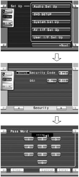
DDX7015/7025/7035
DDX7045/7065
TEST MODE
● Security code writing (E,M,X,C type only)
Security code writing for the unit that control for pair with serial number.
1) How to enter to writing security code
1.Press to Security key when test mode setup screen.
2.Press to Set key When appear on display that security data memory is blank.
3.Security code input to same as normal mode and press to Enter Key on.
Caution : You must security code writing for the unit when control for pair with serial number.
Complete : Writing OK, Writing NG
You can try again adjustment when if appears on writing NG.
Setup Menu screen
Calling security screen
Writing security code screen
24
|
|
|
DDX7015/7025/7035 |
||
|
|
ADJUSTMENT |
DDX7045/7065 |
||
|
|
|
|
|
|
● Chroma IC Adjustment (X14-939) |
|
|
|
||
|
|
|
|
|
|
No. |
Adjustment Item |
Adjustment Method |
Measurement |
Conditions |
|
Locations (X14) |
|
||||
|
|
|
|
|
|
|
|
|
|
|
|
1 |
DC/DC SW frequency |
Connect a frequency counter to the No.8 pin of IC102 (Check land). |
TP925 |
Input signal |
|
|
|
Adjust frequency with VR1(The frequency will be notified later.) |
TP100 (GND) |
: None |
|
|
|
|
|
|
|
2 |
DVD output level |
In the replay mode, replay TDV-540 Title 2 Chapter 6. |
TP653 |
|
|
|
|
Observe the checkland with an oscilloscope and set the output |
TP654 (GND) |
|
|
|
|
level to 2Vp-p. |
|
|
|
|
|
|
|
|
|
3 |
Chroma |
Get into Chroma Adjustment Mode in the Test Mode. |
|
|
|
|
|
|
|
|
|
3-A |
Chroma VCO |
While operating with remote controller, measure the check land |
TP303 |
|
|
|
|
with frequency counter. |
TP944 (GND) |
|
|
|
|
|
|
|
|
3-B |
Brightness |
While operating with remote controller, measure the check land |
TP885 |
10 step NTSC |
|
|
|
|
|
|
|
3-C |
Contrast |
with frequency counter and observe the waveform. |
TP944 (GND) |
input to X34 AV IN |
|
|
|
|
|
|
|
3-D |
Black limiter |
|
|
|
|
|
|
|
|
|
|
3-E |
White limiter |
|
|
|
|
|
|
|
|
|
|
3-F |
Y GCA (Brightness gain) |
|
|
|
|
|
|
|
|
|
|
3-G |
Gamma 1 |
|
|
|
|
|
|
|
|
|
|
3-H |
Gamma 2 |
|
|
|
|
|
|
|
|
|
|
3-I |
R sub-brightness |
|
TP884 |
|
|
|
|
|
TP944 (GND) |
|
|
|
|
|
|
|
|
3-J |
B sub-brightness |
|
TP886 |
|
|
|
|
|
TP944 (GND) |
|
|
|
|
|
|
|
|
3-K |
R sub-contrast |
|
TP884 |
|
|
|
|
|
TP944 (GND) |
|
|
|
|
|
|
|
|
3-L |
B sub-contrast |
|
TP886 |
|
|
|
|
|
TP944 (GND) |
|
|
|
|
|
|
|
|
3-M |
V-COM frequency width |
|
TP869 |
|
|
|
|
|
TP944 (GND) |
|
|
|
|
|
|
|
|
•For adjustment methods on 3-A~3-B, refer to chroma adjustment method.
•As for remote controller operation method, refer to Remote Controller Operation Method.
● Remote Controller Operation Method at Chroma
Adjustment Test Mode
Remote controller uses is the TV/NAVI remote controller AUDIO mode.
1.While pressing EJECT+SRC on the Unit (X14), press RESET key to get into the Test Mode.
2.By operating on the TEST MODE MENU screen, get into the Chroma ADJ mode.
At this time, on the upper left corner of the screen [CH : 16 VCO_FREERUN, VAL : 80] OSD display is made. HEX display.
3.Use 8, 0 on the 10 key to change the setting value. The, the VAL number on upper-left corner of the screen changes.
4.Press PLAY/PAUSE key and confirm on the setting value. When confirmed, [CH : 16 VCO_FREERUN, VAL : 80] the color changes.
When releasing the setting, press on PLAY/PAUSE key again. When released, the color changes.
5.Use 7, 9 keys on the 10 key to set the next one. The CH value changes in the upper-left corner. Repeat the same for Item 3 to 5.
6.When all adjustments are complete, press DIRECT key, which writes the adjustment values to E2PROM. At the same time, it is possible to move out of the Chroma Adjustment mode.
25
DDX7015/7025/7035
DDX7045/7065
ADJUSTMENT
● Chroma Adjustment Method
•While pressing on EJECT+SRC on the Unit (X14), press RESET to enter the Test Mode. (Refer to Remote Controller Operating Method 1.)
•Press DIRECT key on the TV remote controller and get into the Chroma Adjustment mode. (Refer to Remote Controller Operating Method 3.)
•At this point, in the upper left corner of the screen, OSD display of CH : 16, VAL : 80 HEX will appear. (Refer to Remote Controller Operating Method 2.)
•Then, the following adjustment should be conducted. (Refer to Remote Controller Operating Method 3 to 5.)
•After adjusting for each item, press PLAY/PAUSE key to confirm on the selection. (Refer to Remote Controller Operating Method 4.)
No. |
Adjustment Item |
Test Mode |
Adjustment Method |
Adjustment Value |
Condition |
|
|
|
|
|
|
3-A |
Chroma VCO |
CH : 16 |
Using the jig, connect to GND the TP-HD (R382 between R383) |
K : 15.734±50Hz |
Input signal |
|
|
|
and TP-VD (R380 between R381). |
E,M : 15.625±50Hz |
: None |
|
|
|
Adjust the IC303 32pin waveform, using a frequency counter. |
|
|
|
|
|
|
|
|
3-B |
Brightness |
CH : 6 |
Monitor the TP (CN850 59pin) waveform, using an oscilloscope. |
3.2V±0.05V |
Input signal |
|
|
|
Adjust the amplitude value so that the waveform between the |
|
: 10 step (NTSC) |
|
|
|
1 step signal to the negative 1 step signal. |
|
1Vpp V/S ratio |
|
|
|
|
|
|
3-C |
Contrast |
CH : 13 |
Monitor the TP (CN850 59pin) waveform, using an oscilloscope. |
3.0V±0.05V |
: 7 : 3 (75Ω at |
|
|
|
Adjust the amplitude value so that the waveform between the |
|
terminal) |
|
|
|
8 step signal to the negative 8 step signal. |
|
X34 AVIN input |
|
|
|
|
|
|
3-D |
Black limiter |
CH : 5 |
Keep 7F and confirm and then move to the next item. |
7F |
Oscilloscope range |
|
|
|
|
|
|
3-E |
White limiter |
CH : 10 |
Keep 7F and confirm and then move to the next item. |
7F |
: 500mV/DIV AC |
|
|
|
|
|
|
3-F |
Y GCA |
CH : 2 |
Monitor the TP (CN850 59pin) waveform, using an oscilloscope. |
2.45V±0.05V |
|
|
(Brightness gain) |
|
Adjust the amplitude value so that the waveform between the |
|
|
|
|
|
pedestal to the 9 step signal. |
|
|
|
|
|
|
|
|
3-G |
Gamma 1 |
CH : 11 |
Monitor the TP (CN850 59pin) waveform, using an oscilloscope. |
1.1V±0.05V |
|
|
|
|
Adjust the amplitude value so that the waveform between the |
|
|
|
|
|
pedestal to the 2 step signal. |
|
|
|
|
|
|
|
|
3-H |
Gamma 2 |
CH : 12 |
Monitor the TP (CN850 59pin) waveform, using an oscilloscope. |
3.4V±0.05V |
|
|
|
|
Adjust the amplitude value so that the waveform between the |
|
|
|
|
|
pedestal to the 10 step signal. |
|
|
|
|
|
|
|
|
3-I |
R sub-brightness |
CH : 8 |
Monitor the TP (CN850 58pin and 59pin) waveform, using an |
0.1V±0.05V |
|
|
|
|
oscilloscope. |
|
|
|
|
|
It is adjusted so that 58pin signal level higher 0.1V than 59pin |
|
|
|
|
|
signal (for 1 step signal). |
|
|
|
|
|
|
|
|
3-J |
B sub-brightness |
CH : 9 |
Monitor the TP (CN850 60pin and 59pin) waveform, using an |
0.1V±0.05V |
|
|
|
|
oscilloscope. |
|
|
|
|
|
It is adjusted so that 60pin signal level higher 0.1V than 59pin |
|
|
|
|
|
signal (for 1 step signal). |
|
|
|
|
|
|
|
|
26
|
|
|
|
DDX7015/7025/7035 |
||
|
|
|
ADJUSTMENT |
DDX7045/7065 |
||
|
|
|
|
|
|
|
|
|
|
|
|
|
|
No. |
Adjustment Item |
Test Mode |
Adjustment Method |
Adjustment Value |
Condition |
|
|
|
|
|
|
|
|
3-K |
R sub-contrast |
CH : 14 |
Monitor the TP (CN850 58pin and 59pin) waveform, using an |
0.1V±0.05V |
Input signal |
|
|
|
|
oscilloscope. |
|
: 10 step (NTSC) |
|
|
|
|
It is adjusted so that 58pin signal level higher 0.1V than 59pin |
|
1Vpp V/S ratio |
|
|
|
|
signal (for 9 step signal). |
|
: 7 : 3 (75Ω at |
|
|
|
|
|
|
|
|
3-L |
B sub-contrast |
CH : 15 |
Monitor the TP (CN850 60pin and 59pin) waveform, using an |
0.1V±0.05V |
terminal) |
|
|
|
|
oscilloscope. |
|
X34 AVIN input |
|
|
|
|
It is adjusted so that 60pin signal level higher 0.1V than 59pin |
|
Oscilloscope range |
|
|
|
|
signal (for 9 step signal). |
|
: 500mV/DIV AC |
|
|
|
|
|
|
|
|
3-M |
VCOM amplitude |
CH : 1 |
Monitor the TP (CN850 39pin) waveform, using an oscilloscope. |
2.25Vpp±0.05V |
|
|
|
|
|
Adjust the amplitude value so that VCOM square wave. |
|
|
|
|
|
|
|
|
|
|
After adjusting 3-A~3-M and confirming them, press DIRECT key.
At this point, all data is written to the E2PROM. (Refer to Remote Controller Operating Method 6.)
● Video Adjustment (X35-433)
Step |
Items |
Condition |
|
Adjustment / Inspection method |
|||
1 |
Flicker |
Composite |
Boot the unit in the Flicker Adjustment mode. |
||||
|
|
SYNC |
Set the range of oscilloscope to 5mV or less and adjust VR203 so that amplitude of |
||||
|
|
Gray PASTE |
waveform (flicker) will be the smallest. |
||||
|
|
(White 30~50%) |
|
|
|
|
|
|
|
|
|
|
|
|
|
2 |
Touch coordinate |
|
Press the [TOUCH] key in he Test Mode Main screen. Then, starting from the upper left |
|
|
|
andin the order of upper right and lower left, conduct adjustment. |
|
|
|
Confirm on the “Write OK!” display, and press [Return]. |
|
|
|
|
3 |
Screen start point |
Monoscope |
Press on the [Hposi] key on the Test Mode Main screen. |
|
|
(NTSC) |
Use the Graphic1 so that graphic is centered. Adjust with [<<] and [>>] keys. |
|
|
TV reception |
Next, using the Graphic2, with TC1, [<<] and [>>] keys, adjust so that right and left will be |
|
|
|
equal. Then, press on the [NEXT], and adjust on DVD, TV, VIDEO and NAVI one by one |
|
|
|
with [<<] and [>>] keys. |
|
|
|
Finally, confirm on the “Hposi OK” display, and press [Return]. |
|
|
|
Note : |
|
|
|
• When adjusting Graphic1, from TV-SG, input monoscope (NTSC) and adjust. |
|
|
|
• When adjusting TV Screen, connect the TV tuner below. |
|
|
|
• When adjusting NAVI Screen, use DVZ-2200 and adjust with 2-screen display frame. |
27
Loading...