JVC GR-DX25EX, GR-DX25EY, GR-DX25EZ, GR-DX25EK, GR-DX35EX Service Manual
...
SERVICE MANUAL
DIGITAL VIDEO CAMERA
DISASSEMBLY
GR-DX Series
Manual No. |
Model name |
|
|
86735 |
GR-DX25EX,GR-DX25EY,GR-DX25EZ,GR-DX25EK,GR-DX35EX,GR-DX35EY,GR-DX35EZ,GR-DX35EK |
86740 |
GR-DX75EX,GR-DX75EY,GR-DX75EZ,GR-DX75EK,GR-DX95EX,GR-DX95EY,GR-DX95EZ,GR-DX95EK |
86751 |
GR-DX100EX,GR-DX100EY,GR-DX100EZ,GR-DX100EK,GR-DX300EX,GR-DX300EY,GR-DX300EZ,GR-DX300EK |
86752 |
GR-DX45EX,GR-DX45EY,GR-DX45EZ,GR-DX45EK,GR-DX55EX,GR-DX55EY,GR-DX55EZ,GR-DX55EK |
86753 |
GR-DX75AA,GR-DX75AG,GR-DX75AH,GR-DX75AS,GR-DX76AG |
86754 |
GR-DX35AC,GR-DX35AH |
86755 |
GR-DX95AC,GR-DX95AH |
86757 |
GR-DX75US,GR-DX95US |
86762 |
GR-DX106AG |
86763 |
GR-DX300AA,GR-DX300AG |
86764 |
GR-DX300AC,GR-DX300AH |
86765 |
GR-DX75KR,GR-DX95KR |
86766 |
GR-DX300US |
GR-DV Series
Manual No. |
Model name |
|
|
86734 |
GR-DV500US,GR-DV800US,GR-DV801US,GR-DV900US |
86736 |
GR-DV4000US |
86756 |
GR-DV4000EX,GR-DV4000EY,GR-DV4000EZ,GR-DV4000EK |
86758 |
GR-DV700EX,GR-DV700EY,GR-DV700EZ,GR-DV700EK |
86759 |
GR-DV500KR,GR-DV700KR,GR-DV800KR,GR-DV900KR,GR-DV4000KR,GR-DV5000KR |
86760 |
GR-DV400EX,GR-DV400EY, GR-DV500EX,GR-DV500EY,GR-DV500EZ |
86767 |
GR-DV4000AG,GR-DV5000AA,GR-DV5000AG |
86768 |
GR-DV500AA,GR-DV500AG,GR-DV500AS,GR-DV900AA,GR-DV900AG |
86771 |
GR-DV700AH,GR-DV900AC,GR-DV4000AC,GR-DV5000AC |
COPYRIGHT © 2003 VICTOR COMPANY OF JAPAN, LIMITED
No.YF009
2003/12

SECTION 1
DISASSEMBLY (GR-DX Series)
1.1BEFORE ASSEMBLY AND DISASSEMBLY
1.1.1 Precautions
•Be sure to disconnect the power supply unit prior to mounting and soldering of parts.
•Prior to removing a component part that needs to disconnect its connector(s) and its screw(s), first disconnect the wire(s) from the connector(s), and then remove the screw(s).
•When connecting/disconnecting wires, pay enough attention not to damage the connectors.
•When inserting the flat wire to the connector, pay attention to the direction of the flat wire.
•Be careful in removing the parts to which some spacer or shield is attached for reinforcement or insulation.
•When replacing chip parts (especially IC parts), first remove the solder completely to prevent peeling of the pattern.
•Tighten screws properly during the procedures. Unless specified otherwise, tighten screws at a torque of 0.088N·m (0.9kgf·cm). However, 0.088N·m (0.9kgf·cm) is a value at the
time of production. At the time of service, perform the procedure at a torque 10% less than 0.088N·m (0.9kgf·cm). (See "SERVICE NOTE" as for tightening torque.)
1.1.2 Destination of connectors
Two kinds of double-arrows in connection tables respectively show kinds of connector/wires.
: Flat wire |
: Wire |
: Board to board (B-B) |
||||
: The connector of the side to remove |
|
|||||
CONN. No. |
|
CONNECTOR |
|
PIN No. |
||
CN2a |
MAIN |
CN101 |
MONI/BW |
CN761 |
40 |
|
CN2b |
MAIN |
CN103 |
MIC |
CN762 |
2 |
|
1.1.3 Disconnection of connectors (Wires) |
|
|||||
|
Wire |
|
Wire |
|
|
|
|
|
|
|
|
||
|
FPC Connector |
|
Lock |
|
||
|
FPC Connector |
|
||||
|
|
|
|
|||
· Pull both ends of the connector in the arrow |
· Extend the locks in the direction of the arrow for |
|||||
direction, remove the lock and disconnect the flat |
||||||
unlocking and then pull out the wire. After |
||||||
wire. |
|
|
||||
|
|
removing the wire, immediately restore the locks |
||||
|
|
|
||||
|
|
|
to their original positions because the locks are |
|||
B-B Connector |
|
|
apt to come off the connector. |
|
||
|
|
|
|
|
||
|
|
|
|
B-B Connector |
||
B-B Connector |
|
|
|
|
||
· Pull the both ends of the board in the direction of the arrow, and remove the B-B Connector.
Fig.3-1-1
1.1.4 Tools required for disassembly and assembly
Torque driver |
Bit |
Tweezers |
YTU94088 |
YTU94088-003 |
P-895 |
Chip IC replacement jig |
Cleaning cloth |
|
PTS40844-2 |
KSMM-01 |
|
|
Fig.3-1-2 |
|
1-2 (No.YF009) |
|
|
•Torque driver
Be sure to use to fastening the mechanism and exterior parts because those parts must strictly be controlled for tightening torque.
•Bit
This bit is slightly longer than those set in conventional torque drivers.
•Tweezers
To be used for removing and installing parts and wires.
•Chip IC replacement jig
To be used for replacement of IC.
•Cleaning cloth
Recommended cleaning cloth to wipe down the video heads, mechanism (tape transport system), optical lens surface.
1.2ASSEMBLY AND DISASSEMBLY OF MAIN PARTS
1.2.1 Assembly and disassembly
When reassembling, perform the step(s) in reverse order.
STEP |
PART |
Fig. |
POINT |
NOTE |
|
No. |
No. |
||||
|
|
|
|||
|
|
|
|
|
|
|
|
|
|
|
|
[1] |
TOP COVER ASSEMBLY |
Fig.C1 |
S1,2(L1) |
- |
|
[2] |
UPPER ASSEMBLY |
Fig.C2-1 |
S2a,2(S2b),3(S2c) |
- |
|
|
(Inc. VF ASSEMBLY, |
|
2(S2d),S2e,S2c |
|
|
|
SPEAKER/MONITOR) |
|
L2,CN2a,b |
|
|
[8] |
VF ASSEMBLY |
Fig.C2-2 |
2(S8),L8,CN8a |
NOTE 8a |
|
|
|
|
|
NOTE 8b |
|
( 1) |
( 2) |
( 3) |
( 4) |
( 5) |
( 1) Order of steps in Procedure
When reassembling, preform the step(s) in the reverseorder. These numbers are also used as the identification (location) No. of parts Figures.
( 2) Part to be removed or installed.
( 3) Fig. No. showing Procedure or Part Location. C = CABINET
( 4) Identification of part to be removed, unhooked, unlocked, released, unplugged, unclamped or unsoldered.
S = Screw
L = Lock, Release, Hook SD = Solder
CN = Connector
[Example]
•4 (S1a) = Remove four S1a screws.
•3 (L1a) = Disengage three L1a hooks.
•2 (SD1a) = Unsolder two SD1a points.
•CN1a = Remove a CN1a connector.
( 5) Adjustment information for installation.

1.2.2 ASSEMBLY/DISASSEMBLY OF CABINET PARTS AND ELECTRICAL PARTS
zDisassembly procedure
Step |
Parts Name |
Fig. |
Point |
Note |
||
No. |
No. |
|||||
|
|
|
||||
|
|
|
|
|
|
|
|
|
|
|
|
|
|
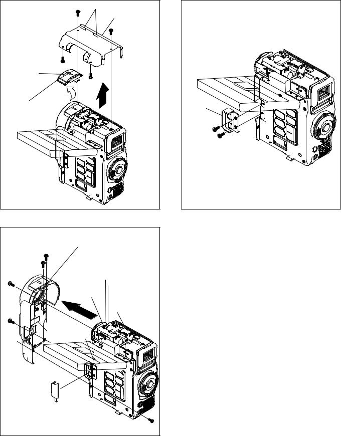
[1] |
COVER(TOP) |
Fig.C1 |
(S1a),3(S1b),2(L1) |
- |
||
|
|
|
|
|
|
|
[2] |
COVER(MIC) |
|
|
L2 |
- |
|
[3] |
FRONT COVER ASSY |
Fig.C2 |
2(S3a),(S3b),(S3c),(S3d),CN3,HOLDER(DV/USB) |
NOTE3a,b,c |
||
[4] |
COVER(DV) |
Fig.C3 |
(S4a),(S4b) |
- |
||
|
|
|
|
|
||
[5] |
UPPER ASSY |
Fig.C4 |
(S5a),(S5b),2(S5c),(S5d),(S5c), |
NOTE5a,b |
||
|
|
|
|
(S5d),(S5e),CN5a,CN5b |
|
|
[6] |
MAIN BOARD ASSY |
Fig.C5-1 |
CN6a,b,c,d,e,(S6a),3(S6b),2(S6c), |
NOTE6a,b |
||
/[7] |
/MECHANISM ASSY |
Fig.C5-2 |
L6a,SHELD PLATE,L6b,CN6f,g,h,i,k,m |
|
||
|
|
|
|
(S7a),3(S7b),BKT(PRE/REC),MECHA BKT ASSY |
- |
|
[8] |
OP BLOCK ASSY |
Fig.C6 |
(S8),BKT(TOP),L8,CN8 |
NOTE8 |
||
/[9] |
/MIC ASSY |
|
|
|
|
|
|
|
|
|
|
||
[10] |
VF ASSY |
Fig.C7 |
CN10,2(S10) |
NOTE10 |
||
NOTE 3a:
Open the CASSETTE COVER, and remove the two screws (No.7 and 8).
NOTE3b:
Take care not to cut the FPC and wire.
NOTE3c:
Be careful about the HOLDER (DV/USB) because it is removed together with the FRONT COVER ASSY.
NOTE5a:
Take care not to damage the part.
NOTE5b:
Take care not to cut the FPC.
NOTE6a:
Remove the MIC wire while removing the MAIN BOARD ASSY.
NOTE6b:
Take care not to cut the FPC.
NOTE8:
Take care not to damage the LENS in OP BLOCK ASSY and not to cut the FPC.
NOTE10:
Take care not to cut the FPC.
zDestination of connectors
CN No. |
|
CONNECTOR |
|
|
Pin. |
||
|
|
|
No. |
||||
|
|
|
|
|
|
|
|
|
|
|
|
|
|
|
|
CN3 |
MAIN |
CN115 |
|
STROBE |
CN6501 |
12 |
|
CN5a |
MAIN |
CN113 |
|
MONITOR |
CN7601 |
49/45 |
|
CN5b |
MAIN |
CN112 |
|
SUB OPE UNIT |
|
- |
9 |
CN6a |
MAIN |
CN101 |
|
BATT.TERM. |
|
- |
17 |
CN6b |
MAIN |
CN109 |
|
SD |
CN301 |
60 |
|
CN6c |
MAIN |
CN102 |
|
CCD |
|
- |
20 |
CN6d |
MAIN |
CN111 |
|
CAMERA OPE UNIT |
- |
11 |
|
CN6e |
MAIN |
CN114 |
|
MIC |
|
- |
4 |
CN6f |
MAIN |
CN106 |
|
SENSOR |
|
- |
16 |
CN6g |
MAIN |
CN110 |
|
HEAD |
|
- |
8 |
CN6h |
MAIN |
CN103 |
|
LOADING MOTOR |
- |
6 |
|
CN6j |
MAIN |
CN107 |
|
ROTARY ENCODER SW |
- |
6 |
|
CN6k |
MAIN |
CN104 |
|
DRUM MOTOR |
|
- |
11 |
CN6m |
MAIN |
CN108 |
|
CAPSTAN MOTOR |
- |
18 |
|
CN8 |
SD |
CN302 |
|
OP BLOCK ASSY |
|
- |
24 |
CN10 |
SD |
CN304 |
|
VF BW |
CN7001 |
18 |
|
|
|
|
|
|
|
|
|
(No.YF009)1-3

1 |
L1 |
|
|
(S1a) |
[1] |
2
(S1b)
3
(S1b)
L2
4
(S1b)
[2]
|
|
Fig.C1 |
|
5 |
[3] |
|
(S3a) |
|
|
6 |
|
7 |
(S3a) |
|
|
a |
|
(S3b) |
|
|
|
|
b |
|
|
NOTE3b |
|
|
CASETTE |
8 |
|
COVER |
(S3c) |
a |
NOTE3a |
|
b |
|
|
NOTE3b CN3 |
|
|
HOLDER(DV/USB) |
|
|
NOTE3c |
|
|
|
9 |
|
|
(S3d) |
|
|
Fig.C2 |
1-4 (No.YF009) |
|
|
[4] |
10 |
(S4a) |
11 |
(S4b) |
Fig.C3 |

NOTE5b [5]
CN5a
CN5b
19 
(S5e)
|
17 |
|
|
|
(S5c) |
13 |
12 |
|
|
(S5b) |
|
16 |
15 |
(S5a) |
|
18 |
|
||
(S5d) |
(S5c) |
|
(S5d)
NOTE5a
14
(S5c)
Fig.C4
23 |
|
|
|
(S6b) |
c |
|
|
NOTE6a |
|
|
|
CN6e |
|
|
|
CN6b |
|
|
|
|
|
|
b |
|
|
a |
22 |
|
20 |
(S6b) |
|
|
21 |
|
|
|
(S6a) |
|
|
|
(S6b) |
|
|
CN6a |
CN6c |
|
|
CN6d |
|
|
|
[6]/[7] |
|
|
|
|
Fig.C5-1 |
|
|
(No.YF009)1-5

|
|
|
24 |
|
|
|
|
SHIELD PLATE |
(S6c) |
25 |
|
[7] |
|
|
|
(S6c) |
||||
|
|
|
|
d |
|
|
|
|
|
|
|
d |
|
|
|
|
L6a |
|
26 |
|
|
|
|
|
|
|
|
|
|
C |
|
e |
(S7a) |
|
|
|
|
|
|
||
|
|
27 |
|
|
|
|
|
|
(S7b) |
28 |
|
e |
|
|
|
CN6m |
(S7b) |
|
BKT(PRE/REC) |
|
|
|
|
|
|||
|
CN6f |
CN6k |
|
|
|
|
|
|
|
|
|
|
|
|
|
|
|
|
b |
|
|
|
CN6g |
|
|
|
|
|
|
CN6j |
29 a |
|
|
|
|
|
|
|
|
|
|
|
|
CN6h (S7b) |
|
MECHA BKT ASSY |
||
|
|
|
|
|
||
|
[6] |
|
|
|
|
|
|
NOTE6b |
|
|
|
: 0.068N.m(0.7kgf.cm) |
|
|
|
L6b |
|
|
|
|
|
|
|
|
|
|
|
|
|
|
Fig.C5-2 |
|
||
[9] |
30 |
|
|
|
|
|
(S8) |
|
|
|
|
|
|
|
|
|
|
|
|
|
|
a |
|
|
|
|
|
|
|
BKT(TOP) |
|
|
CN10 |
a |
|
|
|
|
|
|
|
|
[8] NOTE8 |
|
|
|
NOTE10 |
|
|
|
|
|
|
|
[10] |
|
|
|
|
|
|
b |
|
|
|
|
|
|
31 |
|
|
|
|
|
|
(S10) |
|
|
a |
|
|
|
|
|
|
|
|
|
|
b |
|
CN8 |
|
|
|
|
|
|
|
|
|
|
|
32 |
|
|
|
|
|
|
(S10) |
|
|
|
|
|
|
a |
|
Fig.C6 |
|
|
|
|
Fig.C7 |
1-6 (No.YF009) |
|
|
|
|
|
|
 Loading...