


GR-DVL355EG
Table of contents
 Loading...
JVC GR-DVL355EG, GR-DVL355EK, GR-DVL357EG, GR-DVL357EK, GR-DVL555EG Schematics
...
4-1
SECTION 4
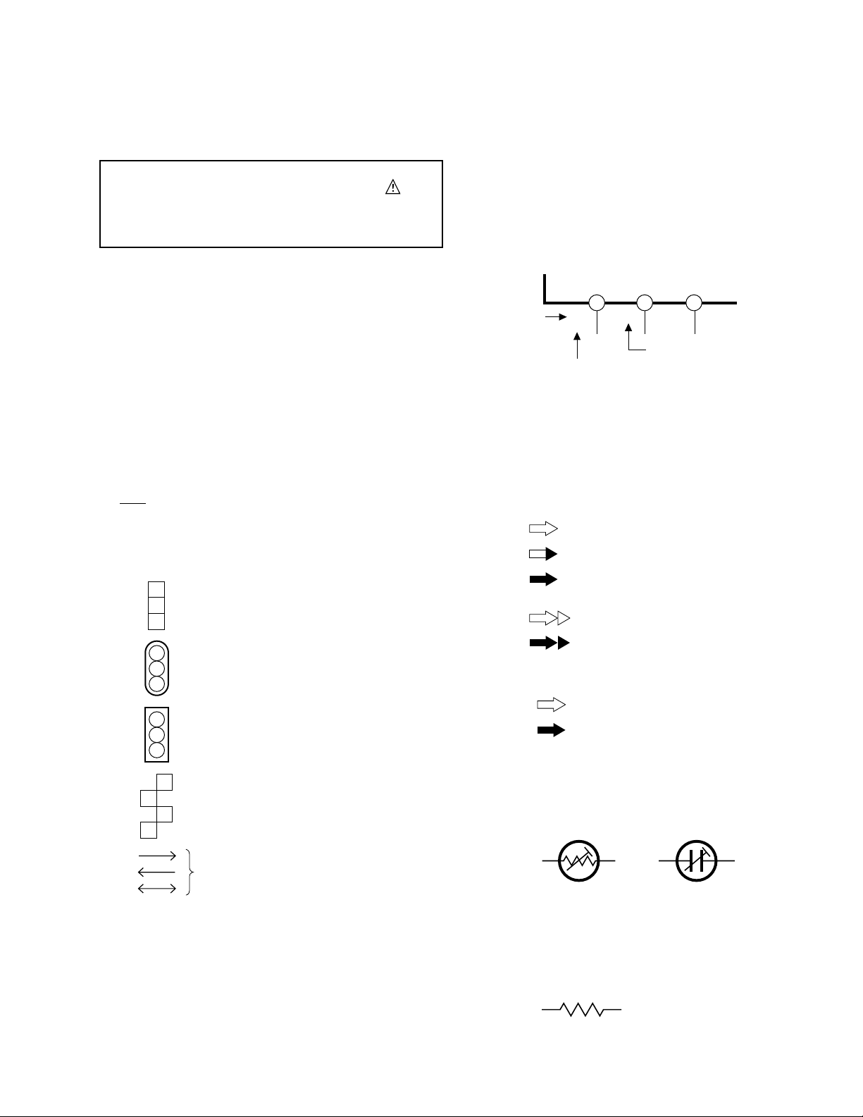
CHARTS AND DIAGRAMS
NOTES OF SCHEMATIC DIAGRAM
Safety precautions
The Components identified by the symbol are
critical for safety. For continued safety, replace safety
critical components only with manufacturer's recom-
mended parts.
1. Units of components on the schematic diagram
Unless otherwise specified.
1) All resistance values are in ohm. 1/6 W, 1/8 W (refer to
parts list).
Chip resistors are 1/16 W.
K: KØ (1000Ø), M: MØ (1000KØ)
2) All capacitance values are in µF, (P: PF).
3) All inductance values are in µH, (m: mH).
4) All diodes are 1SS133, MA165 or 1N4148M (refer to parts
list).
2. Indications of control voltage
AUX : Active at high.
AUX or AUX(L) : Active at low.
3. Interpreting Connector indications
Note: If the voltages are not indicated on the schematic
diagram, refer to the voltage charts.
12 3
2.5
(5.0)
1.8
PB and REC modes
(Voltage of PB and REC modes
are the same)
PB mode
REC mode
4. Voltage measurement
1) Regulator (DC/DC CONV) circuits
REC : Colour bar signal.
PB : Alignment tape (Colour bar).
— : Unmeasurable or unnecessary to measure.
4) Indication on schematic diagram
Voltage Indications for REC and PB mode on the sche-
matic diagram are as shown below.
5. Signal path Symbols
The arrows indicate the signal path as follows.
NOTE : The arrow is DVC unique object.
Playback signal path
Playback and recording signal path
Recording signal path
(including E-E signal path)
Capstan servo path
Drum servo path
(Example)
R-Y
Y
Playback R-Y signal path
Recording Y signal path
6. Indication of the parts for adjustments
The parts for the adjustments are surrounded with the circle as
shown below.
7. Indication of the parts not mounted on the circuit board
“OPEN” is indicated by the parts not mounted on the circuit
board.
R216
OPEN
1
2
3
1
2
3
1
2
3
1
4
2
3
Removable connector
Wire soldered directly on board
Non-removable Board connector
Board to Board
Connected pattern on board
The arrows indicate signal path
S40889-01
4-2
S40889-01
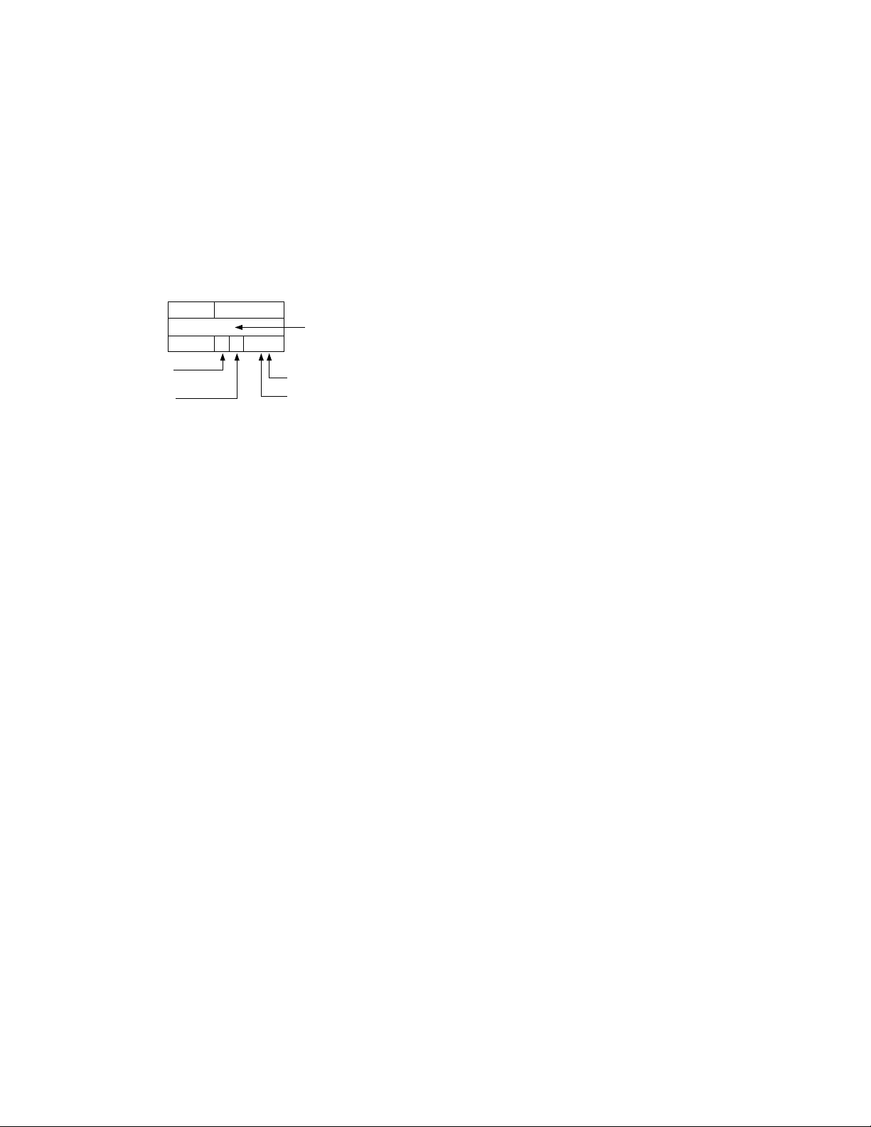
CIRCUIT BOARD NOTES
1. Foil and Component sides
1) Foil side (B side) :
Parts on the foil side seen from foil face (pattern face)
are indicated.
2) Component side (A side) :
Parts on the component side seen from component face
(parts face) indicated.
2. Parts location guides
Parts location are indicated by guide scale on the circuit board.
Note: For general information in service manual, please
refer to the Service Manual of GENERAL INFORMA-
TION Edition 4 No. 82054D (January 1994).
LOCATION
REF No.
IC101 B C 6 A
IC
Category : IC
Horizontal “A” zone
Vertical “6” zone
B : Foil side
(A : Component side)
C : Chip component
D : Discrete component)
1
2
3
5
4
ABCD EFGH
4.1 BOARD INTERCONNECTIONS
4-3 4-4
YTU94074-20
YTU94077-20
(
Page 4-37
)
CN5001
YTU94074-24
YTU94077-24
(
Page 4-27
)
(
Page 4-25
)
OP DRIVE
TG/VDRV
MDA 3.0V
1413
SD WP
GND
VSS
(
GND
)
VDCVF-DS
MON G
VDCVF DS
(
Page 4-33
)
(
Page 4-33
)
(
Page 4-35
)
YTU94109-33
YTU94129A-33
VFREG4.8
BW Y
VD
HD
NSLEED
BW VDD
NC
BW Y
VD
HD
NC
NSLEEP
NC
NC
NC
NC
YTU94074-20
YTU94077-20
CVF G
MMC CD
DSC/USB
(
Page 4-31
)
EXT V IN
(
Page 4-21
)
ANA IN
(
Page 4-38
)
MDA 3.0V
(
Page 4-11
)
PD L
(
Page 4-13
)
YTU94074-6
YTU94077-6
ZOOM UNIT
(
Page 4-41
)
(
Page 4-17
)
DSP
CAM
VTR CPU
VTR CPU
OP DRIVE
B/W VF
MONITOR
VTR CPU
OP DRIVE
(
Page 4-15
)
INV
INH
VTR CPU
XI164SEL
XI164SEL
JUNCTION
(
Page 4-9
)
POW LED
SDET
(
Page 4-5
)
VTR CPU
ZOOM
SDTIN
(
Page 4-7
)(
Page 4-19
)
EXT V IN
D GAIN
(
Page 4-29
)
VTR CPU
(
Page 4-39
)
y10185001a rev0
VDCVF DS
(
Page 4-23
)
(
Page 4-40
)
S DET
D GAIN
YTU94074-15
YTU94077-15
: The number of patch cords
are indicated by interconnected.
NOTE
)
REG 2.5V
INV
VC0
VC1
VC2
BLKA
VC3
BLKB
BLKC
MMC CD
MMC CD
INV
VDC
B SEL
VPPC
RESET
INV
VC0
VC1
VC2
BLKA
VC3
BLKB
BLKC
CHRG LED
RESET
JIG
INV
B SEL
VDC
A CSYNC
A CSYNC
REG_4.8V
GND/DR_GND
JLIP_RX
JLIP_TX
JIG
LCD
(
B/W-VF
)
MODULE
LCD
(
MONITOR
)
MODULE
LCD
(
C-VF
)
MODULE
DC LIGHT
(
DC INPUT CONN.
)
VTR CPU
HGFEDCBA
4
5
3
2
1
MAIN
(
SYSCON
)
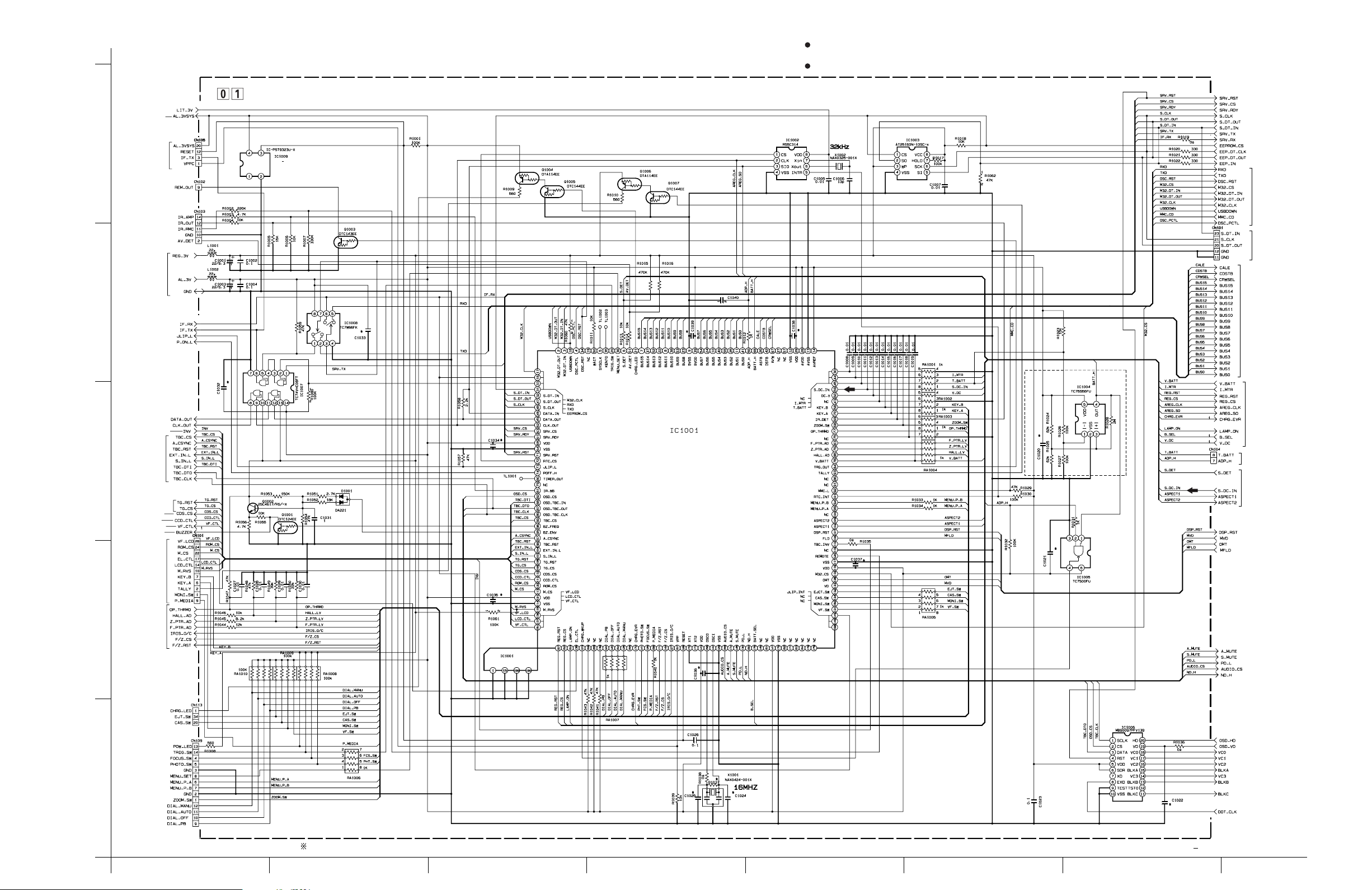
4.2 SYSCON SCHEMATIC DIAGRAM
4-5 4-6
NO WEAR
y10186001a rev0
TO REG
TO REG
TO VTR CPU
,
PC IF
JIG CONN.
TO JACK
CN501
TO JACK
CN502
TO PC IF
TO CAM DSP
,
ANA IN
TO CAM DSP
,
AUDIO
,
TG/VDRV
,
OP DRIVE
TO
ANA IN
TO TG/VDRV
TO CAM DSP
TO TG/VDRV
TO REG
TO AUDIO
TO
MONITOR
CN761
TO
OP DRIVE
TO JUNCTION
CN571
TO
ZOOM UNIT
VCC
VOUT
(
RESET DET
)
NC
GND
C
TO VTR CPU
TO
DSC/USB
TO CAM DSP
TO AUDIO
TO CAM DSP
TO
VOUT
TO MONITOR
CN761
TO
CAM DSP
TO
REG
TO REAR UNIT
CN1
C
When ordering parts
,
be sure to order according to the Part Number indicated in the Parts List.
For the destination of each signal and further line connections that are cut off from
this diagram
,
refer to "4.1 BOARD INTERCONNECTIONS".
NOTES :
UPD703039F1-A03
1
2
3
5
4
ABCD EFGH
NO WEAR
y30121001a rev0
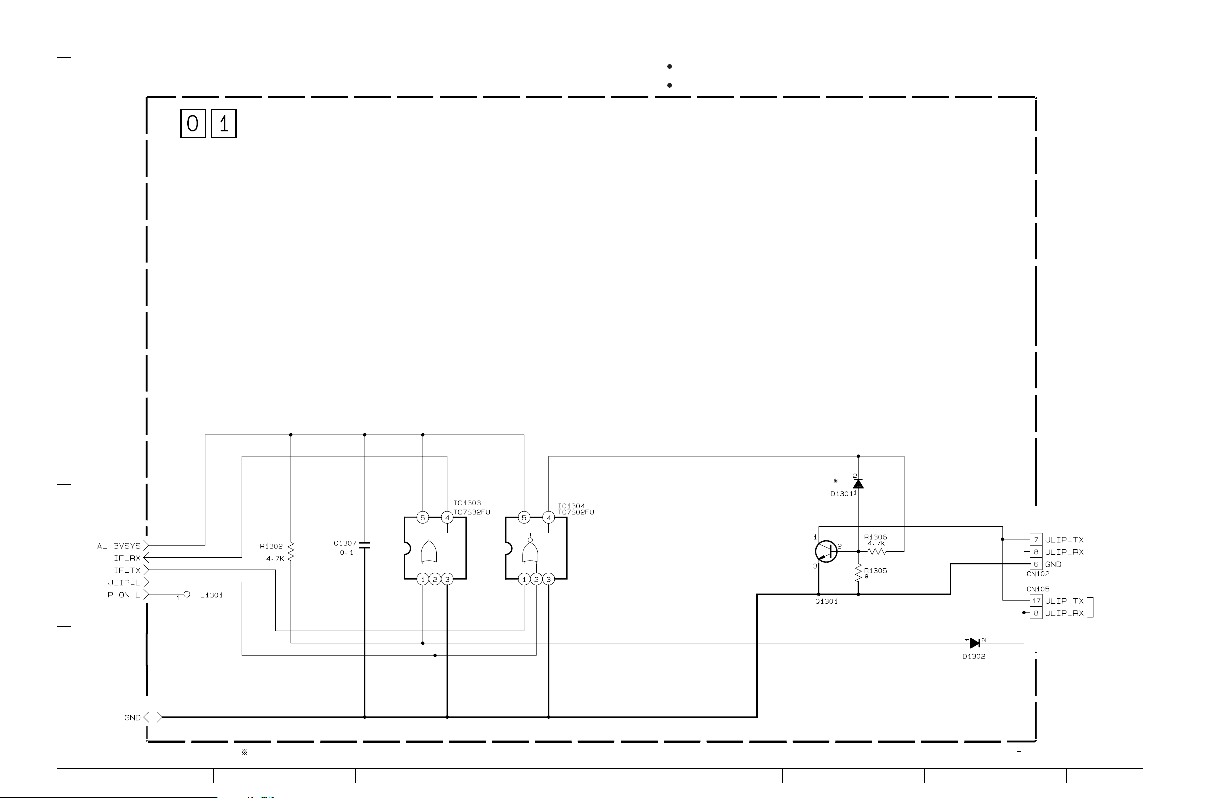
4.3 PC IF SCHEMATIC DIAGRAM
4-7 4-8
TO SYSCON
2SC4617/RS/-X
RB501V-40-X
TO JACK
CN501
JIG CONN.
MAIN
(
PC IF
)
TO REG
When ordering parts
,
be sure to order according to the Part Number indicated in the Parts List.
For the destination of each signal and further line connections that are cut off from
this diagram
,
refer to "4.1 BOARD INTERCONNECTIONS".
NOTES :
HGFEDCBA
4
5
3
2
1
NO WEAR
y10188001a rev0
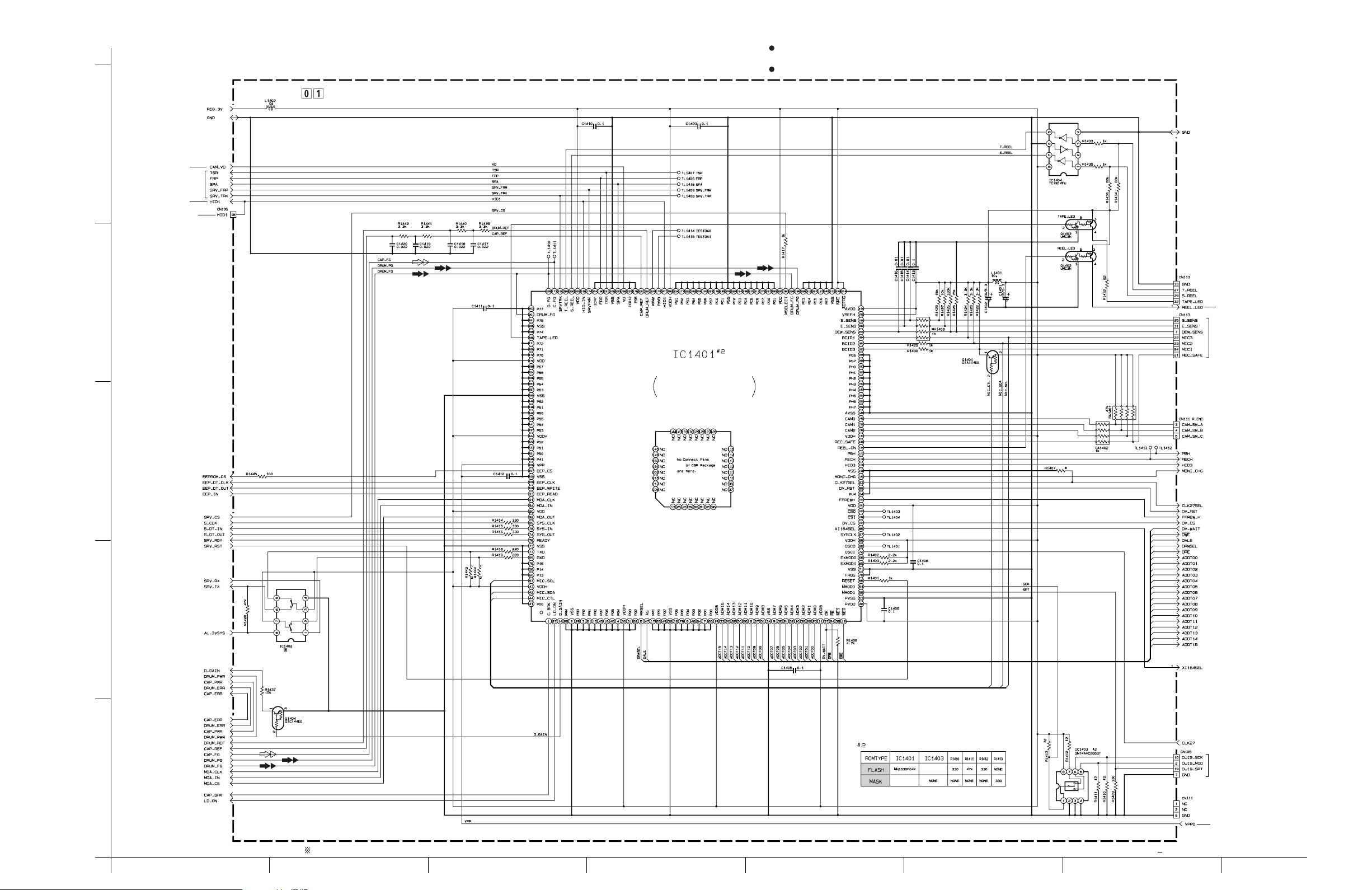
4.4 VTR CPU SCHEMATIC DIAGRAM
4-9 4-10
TO CAM DSP
TO REG
TO DV MAIN
TO DV MAIN
,
PRE/REC
JIG CONN.
TO SYSCON
TO SYSCON
TO SYSCON
TO SYSCON
TO REG
TO MDA
1k
1k
SN74AHC2G53T
TO REG
TO JUNCTION
CN571
TO MDA
TO JUNCTION
CN571
TO
TO PRE/REC
TO DV MAIN
TO DV MAIN
TO TG/VDRV
JIG CONN.
TO
TO REG
ROTARY ENCODER SW
ROTARY ENCODER SW
MN103016KJJ
YQ44882A
MN10316KJJ
MN1030F04KYBJJ
When ordering parts
,
be sure to order according to the Part Number indicated in the Parts List.
For the destination of each signal and further line connections that are cut off from
this diagram
,
refer to "4.1 BOARD INTERCONNECTIONS".
NOTES :
MAIN
(
VTR CPU
)
1
2
3
5
4
ABCD EFGH
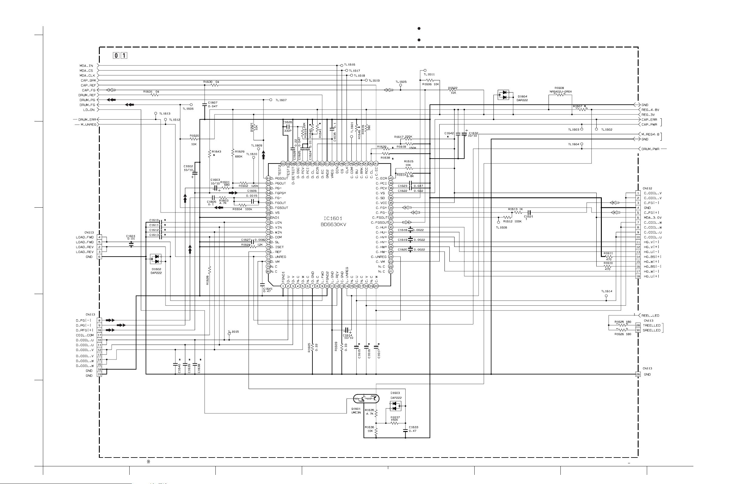
4.5 MDA SCHEMATIC DIAGRAM
4-11 4-12
NO WEAR
y20123001a rev1
TO JUNCTION
TO REG
CN571
TO VTR CPU
TO VTR CPU
TO JUNCTION
CN571
270
TO REG
TO VTR CPU
TO VTR CPU
TO
CAPSTAN MOTOR
TO VTR CPU
TO JUNCTION
CN571
TO JUNCTION
CN571
MAIN
(
MDA
)
TO REG
When ordering parts
,
be sure to order according to the Part Number indicated in the Parts List.
For the destination of each signal and further line connections that are cut off from
this diagram
,
refer to "4.1 BOARD INTERCONNECTIONS".
NOTES :
HGFEDCBA
4
5
3
2
1
NO WEAR
INT MIC
TO
3.3k
y20124001a rev0
TO MONITOR
CN761
TO DV MAIN
TO SYSCON
TO REG
TO JACK
CN502
TO SYSCON
TO SYSCON
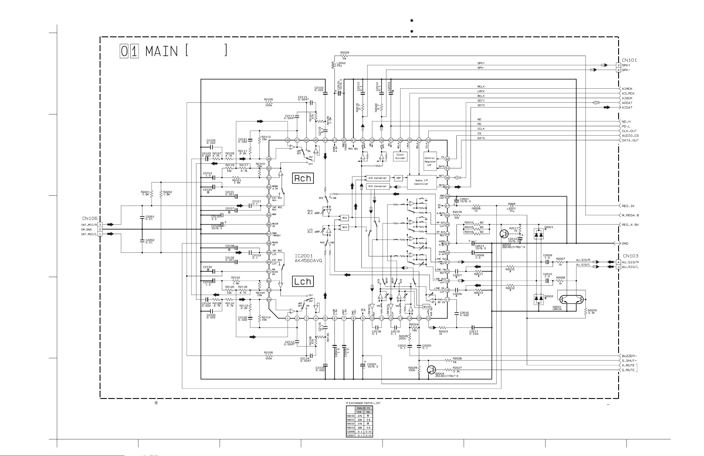
4.6 AUDIO SCHEMATIC DIAGRAM
4-13 4-14
AUDIO
R
L
L
R
R
L
L
L
L
R
R
R
R
L
L
L
R
R
R
L
R
R
R
L
L
R
L
L
TO CAM DSP
When ordering parts
,
be sure to order according to the Part Number indicated in the Parts List.
For the destination of each signal and further line connections that are cut off from
this diagram
,
refer to "4.1 BOARD INTERCONNECTIONS".
NOTES :
1
2
3
5
4
ABCD EFGH
y10196001a rev0
NO WEAR
MAIN
(
DV MAIN
)
PRE/REC
TO REG
TO
ANA IN
TO TG/VDRV
TO AUDIO
TO V TR CP U
JIG CONN.
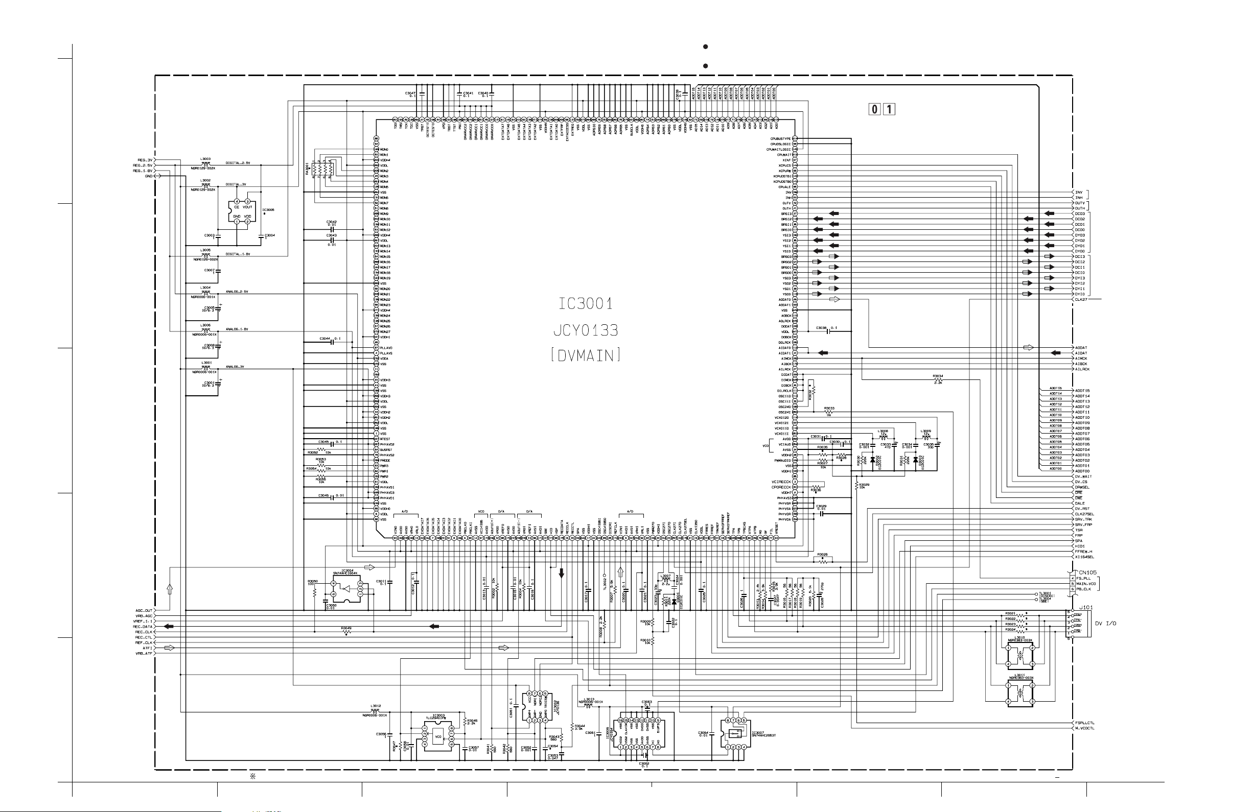
4.7 DV MAIN SCHEMATIC DIAGRAM
4-15 4-16
C
C
Y
Y
C
C
Y
Y
C
C
Y
Y
Y
Y
C
C
Y
C
Y
Y
C
Y
Y
Y
C
C
C
C
Y
Y
C
C
TO CAM DSP
TO CAM DSP
TO CAM DSP
TO CAM DSP
TO CAM DSP
ANA IN
When ordering parts
,
be sure to order according to the Part Number indicated in the Parts List.
For the destination of each signal and further line connections that are cut off from
this diagram
,
refer to "4.1 BOARD INTERCONNECTIONS".
NOTES :
HGFEDCBA
4
5
3
2
1
NO WEAR
y20126001a rev0
VTR CPU
TO
JIG CONN.
TO CAM DSP
TO DV MAIN
TO REG
TO HEAD
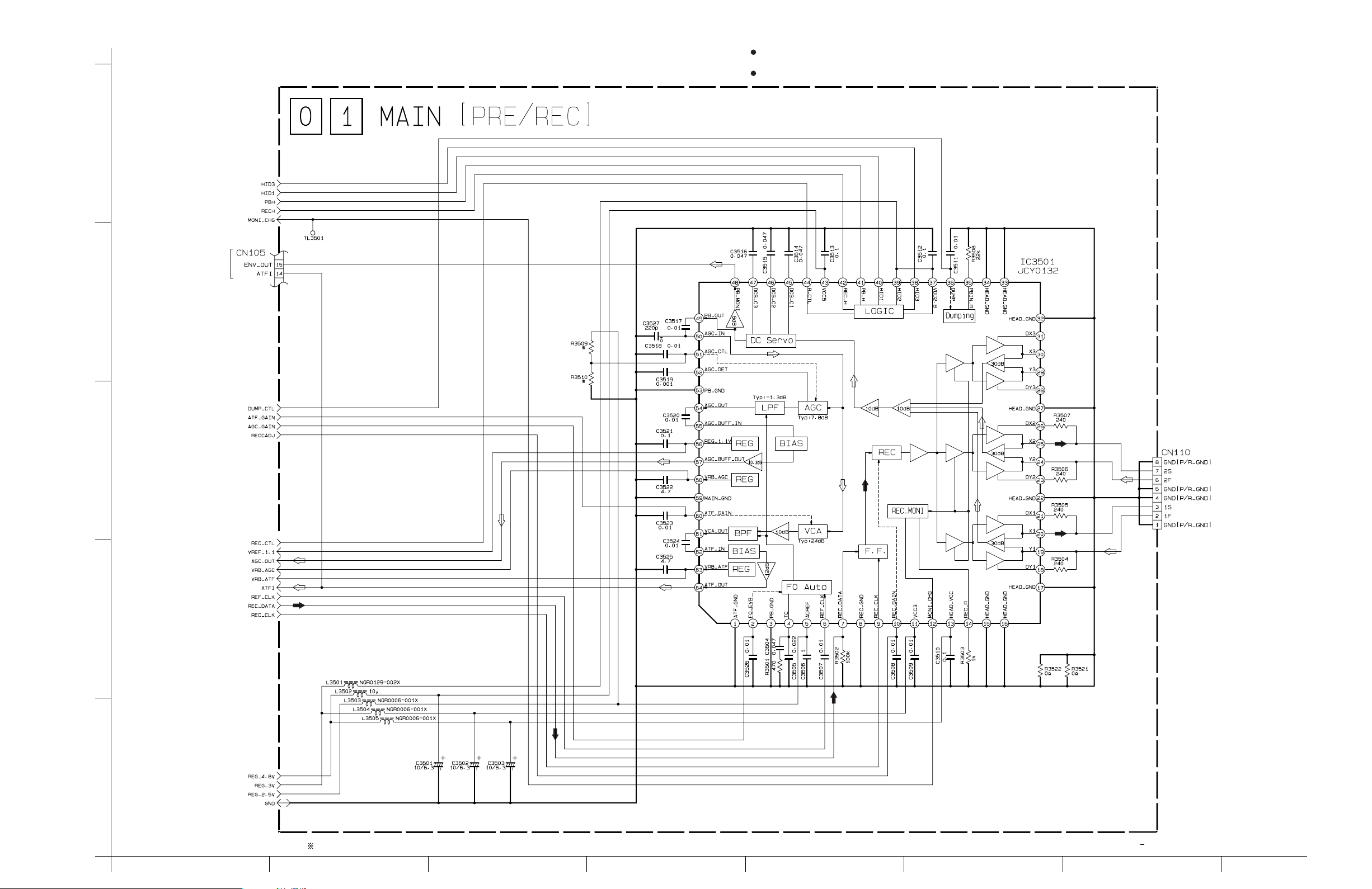
4.8 PRE/REC SCHEMATIC DIAGRAM
4-17 4-18
When ordering parts
,
be sure to order according to the Part Number indicated in the Parts List.
For the destination of each signal and further line connections that are cut off from
this diagram
,
refer to "4.1 BOARD INTERCONNECTIONS".
NOTES :
1
2
3
5
4
ABCD EFGH
NO WEAR
TO ANA IN
TO SYSCON
TO REG
TO CAM DSP
UMT2N
TO ANA IN
TO JACK
CN502
y30123001a rev0
Without ANALOG INPUT
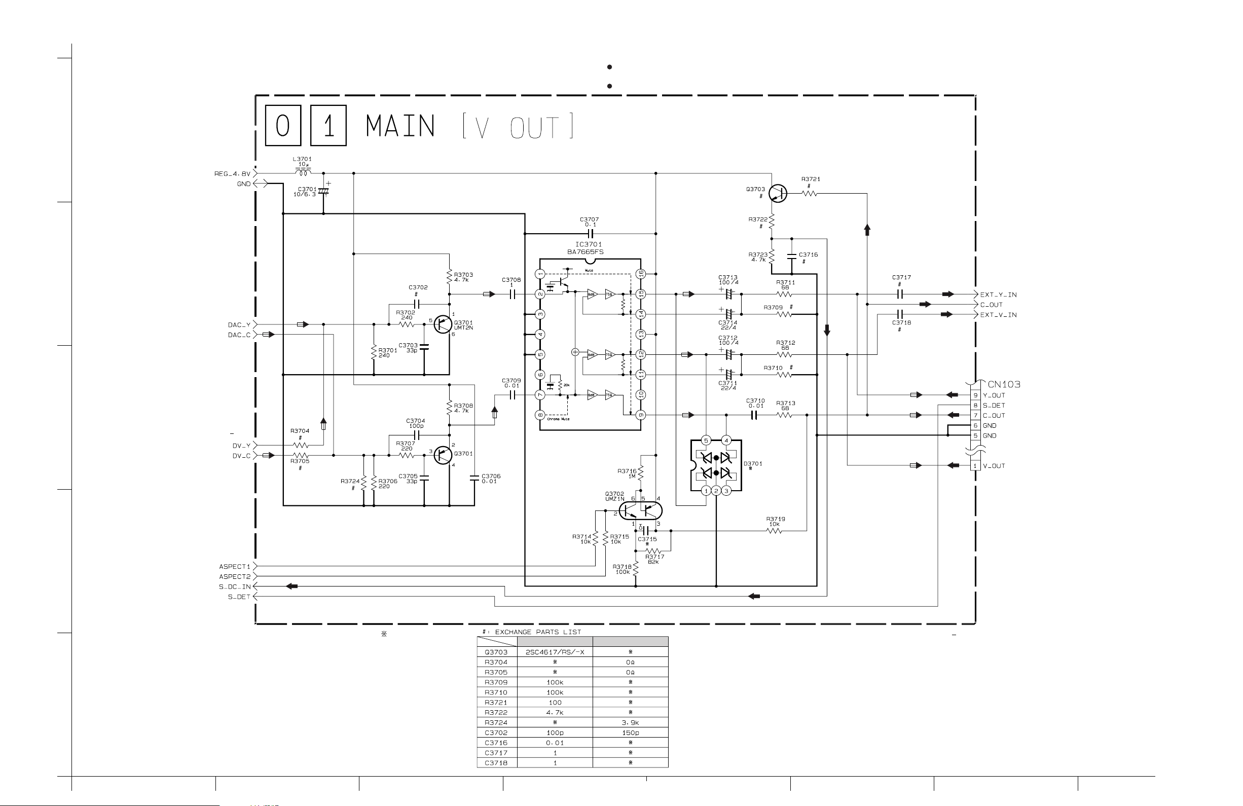
4.9 V OUT SCHEMATIC DIAGRAM
4-19 4-20
Y
C
C
Y
Y
C
Y
Y
CC
C
C
C
C
Y
C
C
Y
With ANALOG INPUT
When ordering parts
,
be sure to order according to the Part Number indicated in the Parts List.
For the destination of each signal and further line connections that are cut off from
this diagram
,
refer to "4.1 BOARD INTERCONNECTIONS".
NOTES :
HGFEDCBA
4
5
3
2
1
4.10
MAIN
(
ANA IN
)
TO
TO V OUT
TO REG
TO TG/VDRV
TO
CAM DSP
TO
DV MAIN
C
Y
Y
C
Y
C
C
C
Y
C
Y
C
C
C
C
Y
Y
Y
Y
C
C
C
Y
Y
Y
Y
C
C
Y
Y
Y
C
Y
C
C
Y
Y
C
C
C
C
Y
Y
NO WEAR
4-21 4-22
CAM DSP
TO SYSCON
TO CAM DSP
TO SYSCON
,
CAM DSP
TO DV MAIN
TO SYSCON
,
DV MAIN
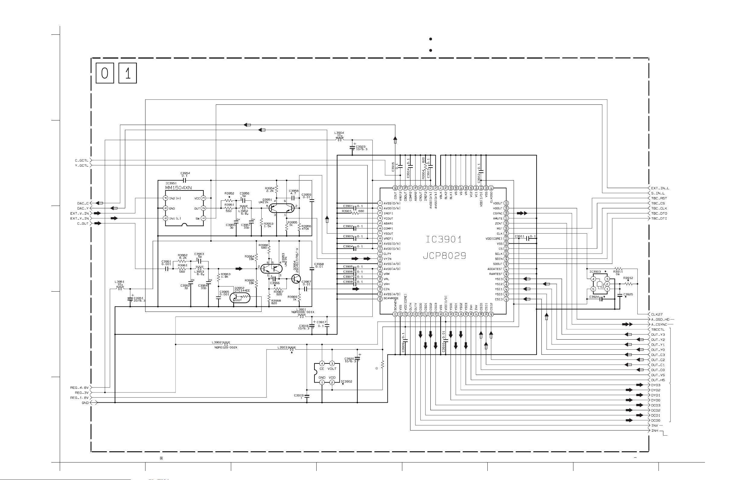
ANA IN SCHEMATIC DIAGRAM [GR-DVL557EG]
When ordering parts
,
be sure to order according to the Part Number indicated in the Parts List.
For the destination of each signal and further line connections that are cut off from
this diagram
,
refer to "4.1 BOARD INTERCONNECTIONS".
NOTES :
R3905
0
y20127001a rev0.1
1
2
3
5
4
ABCD EFGH
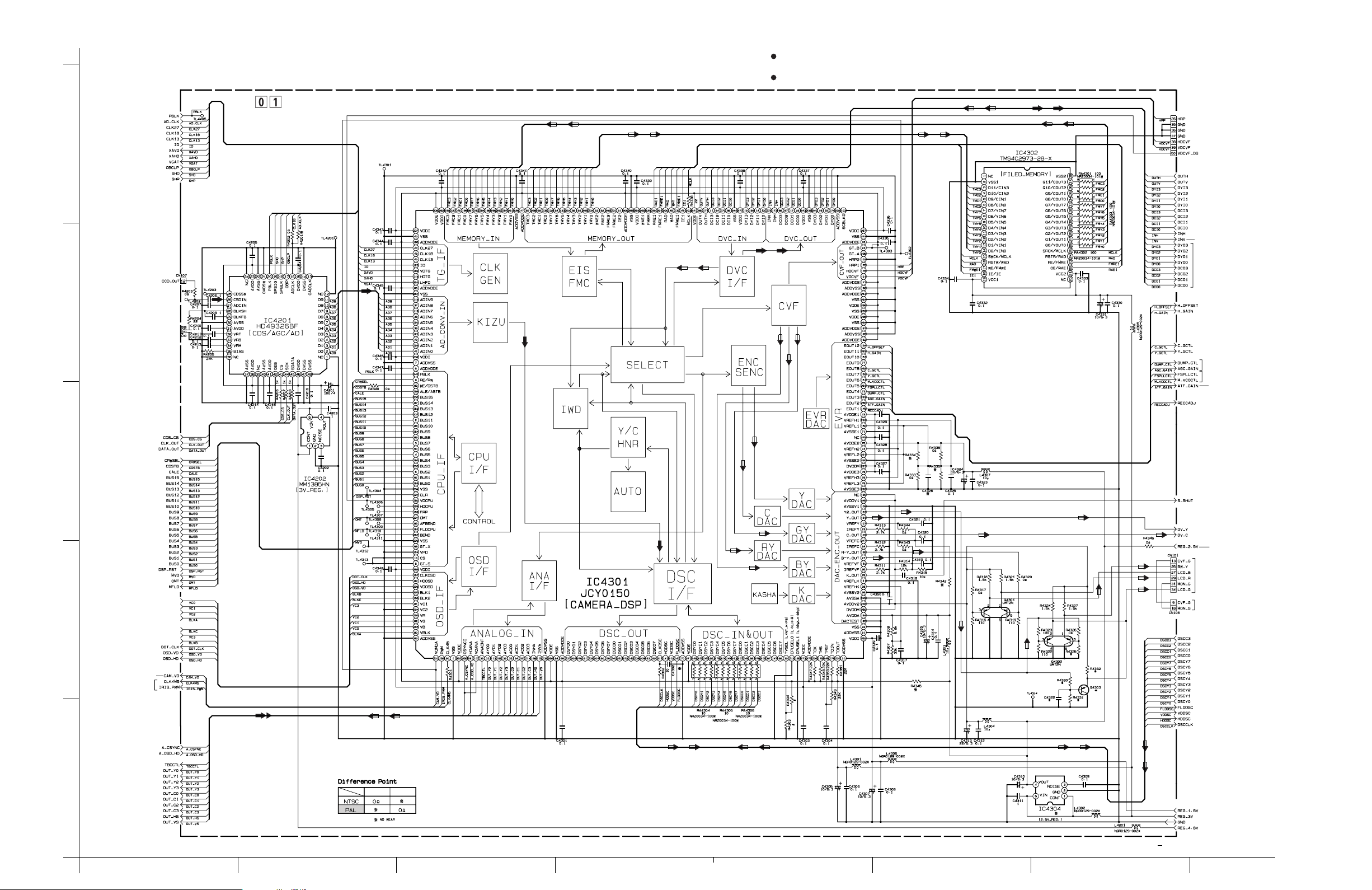
4.11 CAM DSP SCHEMATIC DIAGRAM
4-23 4-24
y10190001a rev0
MAIN
(
CAM DSP
)
TO TG/VDRV
TO CCD
CN5001
R4303 R4304
100
TO SYSCON
TO
OP DRIVE
,
VTR CPU
TO OP DRIVE
TO ANA IN
TO REG
TO MO NITOR
CN761
TO
DV MAIIN
TO OP DRIVE
TO
ANA IN
TO PRE/REC
TO PRE/REC
TO PRE/REC
TO DV MAIN
TO AUDIO
TO MONITOR
CN761
JIG CONN.
TO
YC
CY
YC
YC
YC
CY
CY
CY
YC
Y
B-Y
R-Y
Y
C
YC
YC
YC
Y
B-Y
Y
YC
Y
C
Y
C
Y
R-Y
Y
Y
R-Y
B-Y
Y
R-Y
B-Y
CN101
TOVOUT
TO REG
DSC/USB
VC0
VC1
VC2
BLKA
BLKC
VC3
BLKB
TO DV MAIN
TO SYSCON
,
DV MAIN
When ordering parts
,
be sure to order according to the Part Number indicated in the Parts List.
For the destination of each signal and further line connections that are cut off from
this diagram
,
refer to "4.1 BOARD INTERCONNECTIONS".
NOTES :
Loading...