


 Loading...
DVL355EG/EK,DVL357EG/EK,DVL555EG/EK,DVL557EG/EK-GR
86614 .No
VICTOR COMPANY OF JAPAN, LIMITED |
S40894 |
VIDEO DIVISION |
 Printed in Japan
SERVICE MANUAL
DIGITAL VIDEO CAMERA
GR-DVL355EG/EK, DVL357EG/EK, DVL555EG/EK, DVL557EG/EK
SPECIFICATIONS (The specifications shown pertain specifically to the model GR-DVL150/157/355/357/450/555/557)
|
Camcorder |
For General |
|
Power supply |
: DC 11.0 V } (Using AC Adapter) |
Power consumption |
DC 7.2 V } (Using battery pack) |
|
|
LCD monitor off, viewfinder on |
: Approx. 4.3 W |
LCD monitor on, viewfinder off |
: Approx. 5.3 W |
Video light |
: Approx. 3.5 W |
Dimensions (W x H x D) |
: 83 mm x 97 mm x 188 mm |
|
(with the LCD monitor closed and the viewfinder |
|
pushed down) |
Weight |
: Approx. 610 g |
|
(GR-DVL557/DVL555/DVL450) |
|
Approx. 590 g |
|
(GR-DVL357/DVL355/DVL157/DVL150) |
Operating temperature |
: 0°C to 40°C |
Operating humidity |
: 35% to 80% |
Storage temperature |
: –20°C to 50°C |
Pickup |
: 1/4" CCD |
Lens |
: F 1.8, f = 3.6 mm to 36 mm, 10:1 power zoom lens |
Filter diameter |
: ø37 mm |
LCD monitor |
: 3.5" diagonally measured, LCD panel/TFT active matrix system |
|
(GR-DVL557/DVL555/DVL450) |
|
2.5" diagonally measured, LCD panel/TFT active matrix system |
|
(GR-DVL357/DVL355/DVL157/DVL150) |
Viewfinder |
: Electronic viewfinder with 0.44" colour LCD |
|
(GR-DVL557/DVL555/DVL450) |
|
Electronic viewfinder with 0.24" black/white LCD |
|
(GR-DVL357/DVL355/DVL157/DVL150) |
Speaker |
: Monaural |
For Digital Video Camera |
|
Format |
: DV format (SD mode) |
Signal format |
: PAL standard |
Recording/Playback format |
: Video: Digital component recording |
|
: Audio: PCM digital recording, 32 kHz 4-channel (12-bit), |
|
48 kHz 2-channel (16-bit) |
Cassette |
: Mini DV cassette |
Tape speed |
: SP: 18.8 mm/s |
|
LP: 12.5 mm/s |
Maximum recording time |
: SP: 80 min. |
(using 80 min. cassette) |
LP: 120 min. |
For Digital Still Camera (GR-DVL557/DVL555/DVL357/DVL355 only)
Storage media |
: SD Memory Card/MultiMediaCard |
Compression system |
: JPEG (compatible) |
File size |
: VGA (640 x 480 pixels) |
Picture quality |
: 2 modes (FINE/STANDARD) |
Approximate number of storable images |
|
with memory card [8 MB] (provided) |
|
FINE |
: 100 |
STANDARD |
: 200 |
with memory card [16 MB] (optional) |
|
FINE |
: 200 |
STANDARD |
: 400 |
with memory card [32 MB] (optional) |
|
FINE |
: 400 |
STANDARD |
: 800 |
with memory card [64 MB] (optional) |
|
FINE |
: 800 |
STANDARD |
: 1600 |
For Connectors
S-Video |
|
|
Output |
: Y : |
1 V (p-p), 75 Ø, analogue |
|
C : |
0.29 V (p-p), 75 Ø, analogue |
Input (GR-DVL557 only) |
: Y : |
0.8 V (p-p) – 1.2 V (p-p), 75 Ø, analogue |
AV |
C : |
0.2 V (p-p) – 0.4 V (p-p), 75 Ø, analogue |
|
|
|
Video output |
: 1 V (p-p), 75 Ø, analogue |
|
Video input (GR-DVL557 only) |
: 0.8 V (p-p) – 1.2 V (p-p), 75 Ø, analogue |
|
Audio output |
: 300 mV (rms), 1 kØ, analogue, stereo |
|
Audio input (GR-DVL557 only) |
: 300 mV (rms), 50 kØ, analogue, stereo |
|
DV |
|
Output |
: 4-pin, IEEE 1394 compliant |
Input (GR-DVL557/DVL357/DVL157 only) |
: 4-pin, IEEE 1394 compliant |
USB (GR-DVL557/DVL555/DVL357/DVL355 only) |
: 5-pin |
PC (DIGITAL PHOTO) |
|
(GR-DVL450/DVL157/DVL150 only) |
: ø2.5 mm, 3-pole |
EDIT (GR-DVL557/DVL555/DVL357/DVL355 only) |
: ø3.5 mm, 2-pole |
JLIP (GR-DVL450/DVL157/DVL150 only) |
: ø3.5 mm, 4-pole |
|
AC adapter AP-V10EG |
Power requirement |
: AC 110 V to 240 V`, 50 Hz/60 Hz |
Output |
: DC 11 V } , 1 A |
Dimensions (W x H x D) |
: 59 mm x 31 mm x 84 mm |
Weight |
: Approx. 140 g (not including Power Cord) |
Specifications shown are for SP mode unless otherwise indicated. E & O.E. Design and specifications subject to change without notice.
This service manual is printed on 100% recycled paper. |
No. 86614 |
COPYRIGHT © 2001 VICTOR COMPANY OF JAPAN, LTD. |
February 2001 |

TABLE OF CONTENTS
Section |
Title |
Page |
|
Important Safety Precautions |
|
||
INSTRUCTIONS |
|
||
1. DISASSEMBLY |
|
||
1.1 |
BEFORE ASSEMBLY AND DISASSEMBLY ......................... |
1-1 |
|
1.1.1 |
Precautions ..................................................................... |
1-1 |
|
1.1.2 |
Assembly and disassembly ............................................ |
1-1 |
|
1.1.3 |
Destination of connectors ............................................... |
1-1 |
|
1.1.4 Disconnection of Connectors (Wires) ............................. |
1-1 |
||
1.2 |
JIGS AND TOOLS REQUIRED FOR DISASSEMBLY, |
|
|
|
ASSEMBLY AND ADJUSTMENT .......................................... |
1-2 |
|
1.2.1 Tools required for adjustments ....................................... |
1-2 |
||
1.3 |
DISASSEMBLY/ASSEMBLY OF CABINET PARTS AND |
|
|
|
BOARD ASSEMBLY ............................................................. |
1-2 |
|
1.3.1 |
Disassembly flow chart ................................................... |
1-2 |
|
1.3.2 |
Disassembly method ...................................................... |
1-3 |
|
1.4 |
# MONITOR ASSEMBLY ..................................................... |
1-8 |
|
1.4.1 Disassembly/assembly of monitor assembly |
|
||
|
|
(for 2.5”-type LCD) .......................................................... |
1-8 |
1.4.2 Disassembly/assembly of hinge assembly |
|
||
|
|
(for 2.5”-type LCD) .......................................................... |
1-8 |
1.4.3 Disassembly/assembly of monitor assembly |
|
||
|
|
(for 3.5”-type LCD) .......................................................... |
1-9 |
1.4.4 Disassembly/assembly of hinge assembly |
|
||
|
|
(for 3.5”-type LCD) .......................................................... |
1-9 |
1.5 |
! E. VF ASSEMBLY ........................................................... |
1-10 |
|
1.5.1 Disassembly/assembly of E. VF assembly |
|
||
|
|
(for B/W VF) .................................................................. |
1-10 |
1.5.2 Disassembly/assembly of E. VF assembly |
|
||
|
|
(for Color VF) ................................................................. |
1-11 |
1.6 |
DISASSEMBLY/ASSEMBLY OF OP BLOCK |
|
|
|
ASSEMBLY/CCD BOARD ASSEMBLY .............................. |
1-12 |
|
1.6.1 |
Precautions ................................................................... |
1-12 |
|
1.6.2 How to remove CCD board assembly and CCD base |
|
||
|
|
assembly ...................................................................... |
1-12 |
1.6.3 How to assemble CCD base assembly and CCD board |
|||
|
|
assembly ...................................................................... |
1-12 |
1.6.4 Replacement of Service Repair Parts .......................... |
1-12 |
||
1.7 |
EMERGENCY DISPLAY ..................................................... |
1-13 |
|
1.8 |
SERVICE NOTE ................................................................. |
1-14 |
|
2. MECHANISM ADJUSTMENT |
|
||
2.1 |
PRELIMINARY REMARKS ON ADJUSTMENT AND REPAIR ... |
2-1 |
|
2.1.1 |
Precautions ..................................................................... |
2-1 |
|
2.1.2 Notes on procedure for disassemby/assembly ............... |
2-1 |
||
2.2 |
JIGS AND TOOLS REQUIRED FOR DISASSEMBLY, |
|
|
|
ASSEMBLY AND ADJUSTMENT .......................................... |
2-2 |
|
2.2.1 Tools required for adjustments ....................................... |
2-2 |
||
2.3 |
DISASSEMBLY/ASSEMBLY OF MECHANISM ASSEMBLY 2-3 |
||
2.3.1 |
General statement .......................................................... |
2-3 |
|
2.3.2 Explanation of mechanism mode ................................... |
2-3 |
||
2.3.3 |
Mechanism timing chart .................................................. |
2-4 |
|
2.4 |
Disassembly/assembly of mechanism assembly .................. |
2-5 |
|
2.4.1 |
Follow chart .................................................................... |
2-5 |
|
2.4.2 |
Disassembly/assembly ................................................... |
2-8 |
|
2.4.3 List of procedures for disassembly ............................... |
2-14 |
||
2.5 |
CHECKUP AND ADJUSTMENT OF MECHANISM PHASE 2-15 |
||
2.6 |
MECHANISM ADJUSTMENTS ........................................... |
2-16 |
|
2.6.1 Assembling slide deck assembly and main deck assembly . 2-16
2.6.2 Locating tension pole .................................................... |
2-17 |
|
2.7 |
SERVICE NOTE ................................................................. |
2-18 |
2.8 |
JIG CONNECTOR CABLE CONNECTION ........................ |
2-20 |
3. ELECTRICAL ADJUSTMENT |
|
|
3.1 |
PRECAUTION ...................................................................... |
3-1 |
3.2 |
SETUP .................................................................................. |
3-2 |
Section |
Title |
Page |
|
4. CHARTS AND DIAGRAMS |
|
||
NOTES OF SCHEMATIC DIAGRAM .......................................... |
4-1 |
||
CIRCUIT BOARD NOTES |
........................................................... |
4-2 |
|
4.1 BOARD INTERCONNECTIONS ........................................... |
4-3 |
||
4.2 SYSCON SCHEMATIC .............................................DIAGRAM |
4-5 |
||
4.3 PC IF SCHEMATIC DIAGRAM ................................................... |
4-7 |
||
4.4 |
VTR CPU SCHEMATIC ............................................DIAGRAM |
4-9 |
|
4.5 |
MDA SCHEMATIC DIAGRAM .................................................. |
4-11 |
|
4.6 |
AUDIO SCHEMATIC DIAGRAM ............................................... |
4-13 |
|
4.7 |
DV MAIN SCHEMATIC ...........................................DIAGRAM |
4-15 |
|
4.8 |
PRE/REC SCHEMATIC ..........................................DIAGRAM |
4-17 |
|
4.9 |
V OUT SCHEMATIC DIAGRAM ............................................... |
4-19 |
|
4.10 |
ANA IN SCHEMATIC ................DIAGRAM [GR-DVL557EG] |
4-21 |
|
4.11 |
CAM DSP SCHEMATIC .......................................DIAGRAM |
4-23 |
|
4.12 |
OP DRIVE SCHEMATIC ......................................DIAGRAM |
4-25 |
|
4.13 |
TG/VDRV SCHEMATIC ........................................DIAGRAM |
4-27 |
|
4.14 |
REG SCHEMATIC DIAGRAM ................................................ |
4-29 |
|
4.15 |
DSC/USB SCHEMATIC ........................................DIAGRAM |
4-31 |
|
4.16 |
MONITOR SCHEMATIC .......................................DIAGRAM |
4-33 |
|
4.17 |
LCD BL SCHEMATIC ...........................................DIAGRAM |
4-35 |
|
4.18 |
CCD SCHEMATIC DIAGRAM ................................................ |
4-37 |
|
4.19 |
JUNCTION SCHEMATIC .....................................DIAGRAM |
4-38 |
|
4.20 |
JACK SCHEMATIC DIAGRAM .............................................. |
4-39 |
|
4.21 |
B/W VF SCHEMATIC ...........................................DIAGRAM |
4-40 |
|
4.22 |
ZOOM UNIT SCHEMATIC ...................................DIAGRAM |
4-41 |
|
4.23 |
MAIN CIRCUIT BOARD ......................................................... |
4-43 |
|
4.24 |
MONITOR CIRCUIT BOARD [GR-DVL355EG/EK, |
|
|
|
DVL357EG/EK] ....................................................................... |
|
4-49 |
4.25 |
MONITOR CIRCUIT BOARD [GR-DVL555EG/EK, |
|
|
|
DVL557EG/EK] ....................................................................... |
|
4-51 |
4.26 |
LCD BL CIRCUIT BOARD [GR-DVL355EG/EK, |
|
|
|
DVL357EG/EK] ....................................................................... |
|
4-53 |
4.27 |
LCD BL CIRCUIT BOARD [GR-DVL555EG/EK, |
|
|
|
DVL557EG/EK] ....................................................................... |
|
4-55 |
4.28 |
CCD AND JUNCTION ............................CIRCUIT BOARDS |
4-57 |
|
4.29 |
JACK CIRCUIT BOARD ......................................................... |
4-59 |
|
4.30 |
VOLTAGE CHARTS ............................................................... |
|
4-61 |
4.31 |
POWER SYSTEM BLOCK ...................................DIAGRAM |
4-67 |
|
4.32 |
VIDEO SYSTEM BLOCK ......................................DIAGRAM |
4-69 |
|
4.33 |
REGULATOR SYSTEM ..........................BLOCK DIAGRAM |
4-73 |
|
4.34 |
AUDIO SYSTEM BLOCK .....................................DIAGRAM |
4-75 |
|
5. PARTS LIST |
|
|
|
5.1 PACKING AND ACCESSORY ...............ASSEMBLY <M1> |
5-1 |
||
5.2 FINAL ASSEMBLY <M2> ..................................................... |
5-3 |
||
5.3 MECHANISM ASSEMBLY .........................................<M3> |
5-6 |
||
5.4 ELECTRONIC VIEWFINDER ASSEMBLY <M4> |
|
||
|
[GR-DVL555EG/EK, 557EG] ................................................ |
5-8 |
|
5.4 ELECTRONIC VIEWFINDER ASSEMBLY <M4> |
|
||
|
[GR-DVL355EG/EK, 357EG/EK, ..............................557EK] |
5-9 |
|
5.5 MONITOR ASSEMBLY <M5> |
|
||
|
[GR-DVL355EG/EK, 357EG/EK] ........................................ |
5-10 |
|
5.5 MONITOR ASSEMBLY <M5> |
|
||
|
[GR-DVL555EG/EK, 557EG/EK] ......................................... |
5-11 |
|
5.6 ELECTRICAL PARTS .................................................LIST |
5-12 |
||
MONITOR BOARD ASSEMBLY .....................................<02> |
5-21 |
||
LCD BL BOARD ASSEMBLY .........................................<03> |
5-23 |
||
CCD BOARD ASSEMBLY ..............................................<04> |
5-23 |
||
JUNCTION BOARD ASSEMBLY ...................................<05> |
5-23 |
||
JACK BOARD ASSEMBLY ............................................<06> |
5-23 |
||
The following table lists the differing points between Models GR-DVL355EG/EK,GR-DVL357EG/EK,GR-DVL555EG/EK and GR-DVL557EG/EK in this series.
|
GR-DVL355EG |
GR-DVL355EK |
GR-DVL357EG |
GR-DVL357EK |
GR-DVL555EG |
GR-DVL555EK |
GR-DVL557EG |
GR-DVL557EK |
|
|
|
|
|
|
|
|
|
|
|
|
|
|
|
|
|
|
VIEW FINDER |
B/W |
B/W |
B/W |
B/W |
COLOR |
COLOR |
COLOR |
B/W |
LCD MONITOR |
2.5” |
2.5” |
2.5” |
2.5” |
3.5” |
3.5” |
3.5” |
3.5” |
AV IN |
NOT USED |
NOT USED |
NOT USED |
NOT USED |
NOT USED |
NOT USED |
USED |
NOT USED |
S IN |
NOT USED |
NOT USED |
NOT USED |
NOT USED |
NOT USED |
NOT USED |
USED |
NOT USED |
DV IN |
NOT USED |
NOT USED |
USED |
USED |
NOT USED |
NOT USED |
USED |
NOT USED |
AC ADAPTER |
AP-V10EG |
AP-V10EK |
AP-V10EG |
AP-V10EK |
AP-V10EG |
AP-V10EK |
AP-V10EG |
AP-V10EK |
Important Safety Precautions
Prior to shipment from the factory, JVC products are strictly inspected to conform with the recognized product safety and electrical codes of the countries in which they are to be sold. However, in order to maintain such compliance, it is equally important to implement the following precautions when a set is being serviced.
•Precautions during Servicing |
|
||
1. Locations requiring special caution are denoted by labels and in- |
12. Crimp type wire connector |
||
scriptions on the cabinet, chassis and certain parts of the product. |
In such cases as when replacing the power transformer in sets |
||
When performing service, be sure to read and comply with these |
where the connections between the power cord and power trans- |
||
and other cautionary notices appearing in the operation and serv- |
former primary lead wires are performed using crimp type connec- |
||
ice manuals. |
|
|
tors, if replacing the connectors is unavoidable, in order to prevent |
|
|
|
safety hazards, perform carefully and precisely according to the |
2. Parts identified by the ! symbol and shaded ( |
|
|
|
|
) parts are |
following steps. |
|
critical for safety. |
|
|
1) Connector part number : E03830-001 |
Replace only with specified part numbers. |
|
|
|
Note: Parts in this category also include those specified to com- |
2) Required tool : Connector crimping tool of the proper type which |
||
ply with X-ray emission standards for products using |
will not damage insulated parts. |
||
cathode ray tubes and those specified for compliance |
3) Replacement procedure |
||
with various regulations regarding spurious radiation |
(1) Remove the old connector by cutting the wires at a point |
||
emission. |
|
|
close to the connector. |
|
|
|
Important : Do not reuse a connector (discard it). |
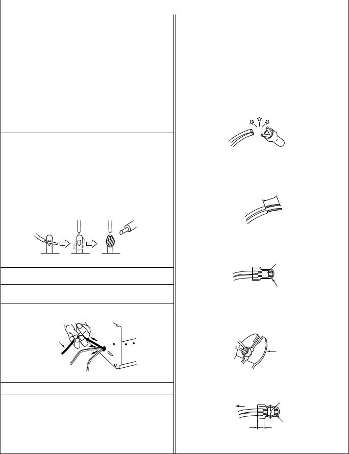
3.Fuse replacement caution notice.
Caution for continued protection against fire hazard.
Replace only with same type and rated fuse(s) as specified.
4. Use specified internal wiring. Note especially:
1) Wires covered with PVC tubing
2) Double insulated wires cut close to connector
3) High voltage leads
|
|
|
|
|
|
Fig.3 |
|
5. |
Use specified insulating materials for hazardous live parts. Note |
(2) Strip about 15 mm of the insulation from the ends of the |
|||||
|
especially: |
|
|
|
|||
|
1) |
Insulation Tape |
3) |
Spacers |
5) Barrier |
wires. If the wires are stranded, twist the strands to avoid |
|
|
2) |
PVC tubing |
4) |
Insulation sheets for transistors |
frayed conductors. |
||
|
|
|
|
|
|
15 mm |
|
6. |
When replacing AC primary side components (transformers, power |
||||||
|
|||||||
|
cords, noise blocking capacitors, etc.) wrap ends of wires securely |
|
|||||
|
about the terminals before soldering. |
|
|
||||
|
|
|
Fig.4 |
|
|
|
(3) Align the lengths of the wires to be connected. Insert the |
||
|
|
wires fully into the connector. |
|
|
|
Fig.1 |
|
Metal sleeve |
|
7. |
Observe that wires do not contact heat producing parts (heatsinks, |
|
|
|
|
oxide metal film resistors, fusible resistors, etc.) |
|
|
|
8. |
Check that replaced wires do not contact sharp edged or pointed |
|
Connector |
|
|
parts. |
|
Fig.5 |
|
|
|
|
|
|
9. |
When a power cord has been replaced, check that 10-15 kg of |
(4) As shown in Fig.6, use the crimping tool to crimp the metal |
||
|
force in any direction will not loosen it. |
|||
|
sleeve at the center position. Be sure to crimp fully to the |
|||
|
|
|||
|
|
complete closure of the tool. |
|
|
|
Power cord |
|
|
|
|
|
|
25 |
Crimping tool |
|
|
|
1. |
|
|
|
2. |
|
|
|
|
5. |
0 |
|
|
|
|
|
|
|
|
5 |
|
|
|
Fig.2 |
|
Fig.6 |
|
10. |
Also check areas surrounding repaired locations. |
(5) Check the four points noted in Fig.7. |
||
11. |
Products using cathode ray tubes (CRTs) |
Not easily pulled free |
Crimped at approx. center |
|
|
of metal sleeve |
|||
|
In regard to such products, the cathode ray tubes themselves, the |
|
|
|
|
|
|
|
|
|
high voltage circuits, and related circuits are specified for compli- |
|
|
|
|
ance with recognized codes pertaining to X-ray emission. |
|
|
|
|
Consequently, when servicing these products, replace the cath- |
|
|
Conductors extended |
|
ode ray tubes and other parts with only the specified parts. Under |
Wire insulation recessed |
|
|
|
no circumstances attempt to modify these circuits. |
|
||
|
more than 4 mm |
|
||
|
Unauthorized modification can increase the high voltage value and |
|
||
|
|
Fig.7 |
|
|
|
cause X-ray emission from the cathode ray tube. |
|
|
|
I |
S40888-01 |
•Safety Check after Servicing
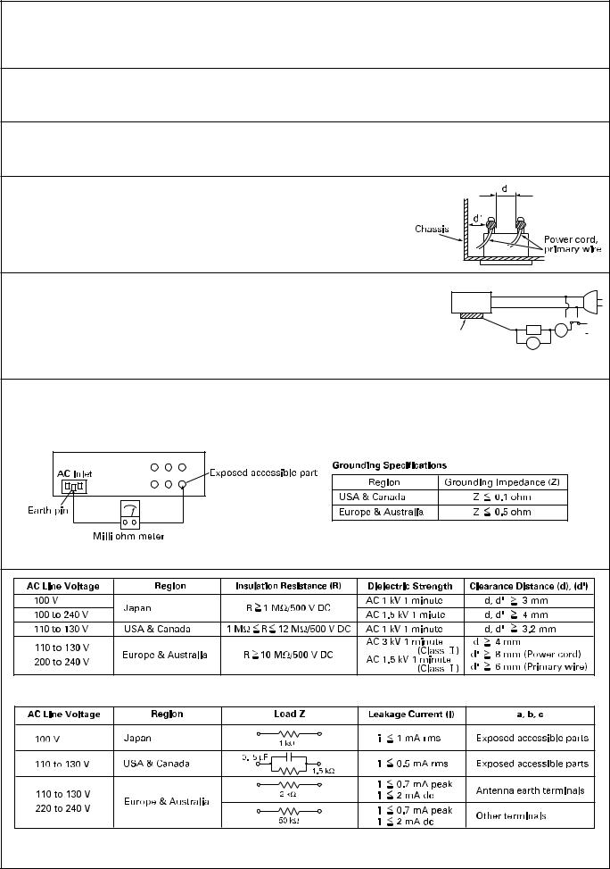
Examine the area surrounding the repaired location for damage or deterioration. Observe that screws, parts and wires have been returned to original positions, Afterwards, perform the following tests and confirm the specified values in order to verify compliance with safety standards.
1.Insulation resistance test
Confirm the specified insulation resistance or greater between power cord plug prongs and externally exposed parts of the set (RF terminals, antenna terminals, video and audio input and output terminals, microphone jacks, earphone jacks, etc.). See table 1 below.
2.Dielectric strength test
Confirm specified dielectric strength or greater between power cord plug prongs and exposed accessible parts of the set (RF terminals, antenna terminals, video and audio input and output terminals, microphone jacks, earphone jacks, etc.). See table 1 below.
3. Clearance distance
When replacing primary circuit components, confirm specified clearance distance (d), (d’) between soldered terminals, and between terminals and surrounding metallic parts. See table 1 below.
Fig. 8
4.Leakage current test
Confirm specified or lower leakage current between earth ground/power cord plug prongs and externally exposed accessible parts (RF terminals, antenna terminals, video and audio input and output terminals, microphone jacks, earphone jacks, etc.).
Measuring Method : (Power ON)
Insert load Z between earth ground/power cord plug prongs and externally exposed accessible parts. Use an AC voltmeter to measure across both terminals of load Z. See figure 9 and following table 2.
a
 b
b
Z A c 
Externally exposed V
accessible part
Fig. 9
5.Grounding (Class 1 model only)
Confirm specified or lower grounding impedance between earth pin in AC inlet and externally exposed accessible parts (Video in, Video out, Audio in, Audio out or Fixing screw etc.).
Measuring Method:
Connect milli ohm meter between earth pin in AC inlet and exposed accessible parts. See figure 10 and grounding specifications.
Fig. 10
Table 1 Specifications for each region
Table 2 Leakage current specifications for each region
Note: These tables are unofficial and for reference only. Be sure to confirm the precise values for your particular country and locality.
II |
S40888-01 |
|
SECTION 1
DISASSEMBLY
1.1 BEFORE ASSEMBLY AND DISASSEMBLY
1.1.1 Precautions
1.Be sure to remove the power supply unit prior to mounting and soldering of parts.
2.When removing a component part that needs to disconnect the connector and to remove the screw for removing itself, first disconnect the connecting wire from the connector and then remove the screw beforehand.
3.When connecting and disconnecting the connectors, be careful not to damage the wire.
4.Carefully remove and handle the part to which some spacer or shield is attached for reinforcement or insulation.
5.When replacing chip parts (especially IC parts), desolder completely first (to prevent peeling of the pattern).
6.Tighten screws properly during the procedures. Unless specified otherwise, tighten screws at a torque of 0.069N•m(0.7kgf•cm).
1.1.2 |
Assembly and disassembly |
|
|
|||||||
STEP |
PART |
Fig.No. |
POINT |
NOTE |
||||||
No. |
||||||||||
|
|
|
|
|
|
|
|
|||
|
|
|
|
|
|
|
|
|
|
|
1 |
COVER(ZOOM) |
Fig.1-3-1 |
(S1a),(S1b),2(L1a),2(L1b ) |
- |
||||||
|
|
ASSY |
|
|
|
|
|
|
||
2 |
UPPER CASE ASSY |
Fig.1-3-2 |
(S2a),(S2b),(L2),(S2c) |
NOTE2 |
||||||
|
|
( Inc.E.VF UNIT |
|
|
2(S2a),(S2d),4(S2a) |
|
|
|||
|
|
(B/W,COLOR), |
|
|
CAP(DC JACK) |
|
|
|||
|
|
SPEAKER/ |
|
|
CN 2a |
|
|
|||
|
|
MONITOR) |
|
|
|
|
|
|
||
|
|
|
|
|
|
|
|
|
||
|
|
|
|
|
|
|
|
|
|
|
|
|
|
|
|
|
|
|
|
|
|
(1) |
(2) |
(3) |
(4) |
(5) |
||||||
(1)Indicate the disassembly steps. When assembling, perform in the reverse order of these steps. This number corresponds to the number in the disassembly diagram.
(2)Indicates the name of disassembly/assembly parts.
(3)Indicates the number in the disassembly diagram.
(4)Indicates parts and points such as screws, washers, springs which must be removed during disassembly/ assembly.
Symbol |
Name, Point |
S |
Screw |
L |
Lock, Pawl, Hook |
SD |
Soldering |
(Others) |
Connector, Cover, Bracket, etc. |
(Example)
•2 (S1) : Remove the two screws (S1) for removing the part 1.
•CN 2a : Disconnect the connector 2a .
• SD1 : Unsolder at the point SD1.
(5) Precautions on disassembly/assembly.
1.1.3 Destination of connectors
Note: Three kinds of double-arrows in connection tables respectively show kinds of connector/wires.
↔ : Wire
: Flat wire
 : Board to Board connector [Example]
Note: Remove the parts marked in  .
.
CONN. |
|
CONNECTOR |
|
Pin No. |
||
No. |
|
|
||||
|
|
|
|
|
|
|
|
|
|
|
|
|
|
2a |
MAIN |
CN101 |
|
MONITOR |
CN761 |
50 |
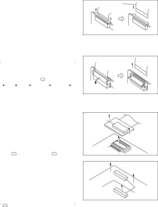
1.1.4 Disconnection of Connectors (Wires)
Connector
Pull both ends of the connector in the arrow direction, remove the lock and disconnect the flat wire.
Flat wire
Connector
Fig. 1-1-1 Connector 1
Extend the locks in the direction of the arrow for unlocking and then pull out the wire. After removing the wire, immediately restore the locks to their original positions because the locks are apt to come off the connector.
Flat wire 
Connector
Fig. 1-1-2 Connector 2
B-B connector
Pull the board by both the sides in the direction of the arrow for disconnecting the B-B connector.
Connector
Connector |
Fig. 1-1-3 Connector 3 |
Connector |
Fig. 1-1-4 Connector 4 |
1-1
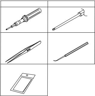
1.2JIGS AND TOOLS REQUIRED FOR DISASSEMBLY, ASSEMBLY AND ADJUSTMENT
1.2.1 Tools required for adjustments
1 |
Torque Driver |
2 |
Bit |
|
YTU94088 |
YTU94088-003 |
|||
|
|
3 |
Tweezers |
4 |
Chip IC Replacement Jig |
|
P-895 |
PTS40844-2 |
|||
|
|
5 |
Cleaning Cloth |
|
KSMM-01 |
||
|
Table 1-2-1
1.Torque driver
Be sure to use to fastening the mechanism and exterior parts because those parts must strictly be controlled for tightening torque.
2.Bit
This bit is slightly longer than those set in conventional torque drivers.
3.Tweezers
To be used for removing and installing parts and wires.
4.Chip IC replacement jig
To be used for adjustment of the camera system.
5.Cleaning cloth
Recommended cleaning cloth to wipe down the video heads, mechanism (tape transport system), optical lens surface.
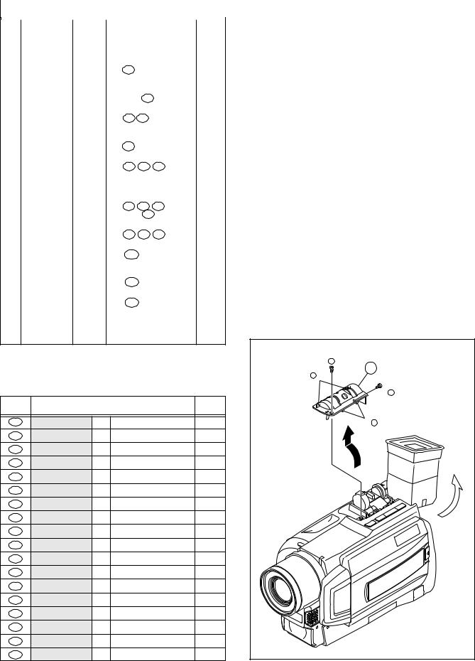
1.3DISASSEMBLY/ASSEMBLY OF CABINET PARTS AND BOARD ASSEMBLY
1.3.1 Disassembly flow chart
This flowchart indicates the disassembly step for the cabinet parts and board assembly in order to gain access to item(s) to be serviced. When reassembling, perform the step(s) in reverse order.
1 |
|
COVER(ZOOM) ASSY |
||
|
|
|
||
|
|
|
|
|
2 |
|
UPPER CASE ASSY |
||
|
(Inc.E.VF UNIT(B/W,COLOR),SPEAKER/MONITOR) |
|||
|
|
|
||
|
|
|
|
|
3 |
|
FRONT COVER ASSY |
||
|
(Inc.DC LIGHT,MIC) |
|||
|
|
|||
|
|
|
||
|
|
|
|
|
4 |
|
OP BLOCK ASSY |
||
|
/BRACKET(OP) ASSY |
|||
|
|
|||
5 |
|
|
||
|
|
|
||
|
REAR UNIT |
|||
|
|
|
||
|
|
|
|
|
6 |
|
LOWER CASE ASSY |
||
/ |
|
(Inc.ZOOM UNIT) |
||
7 |
|
/JACK BOARD ASSY |
||
|
|
|
|
|
8 |
|
JUNCTION BOARD ASSY |
||
8 |
|
|
|
|
|
|
|
||
MAIN BOARD ASSY |
||||
/ |
|
|||
|
/MECHANISM ASSY |
|||
0 |
|
|||
|
|
|
||
! |
|
|
|
|
|
E.VF UNIT |
|||
/ |
|
|||
|
/SPEAKER |
|||
@ |
|
|||
|
|
|
||
# |
|
|
|
|
|
MONITOR ASSY |
|||
/ |
|
|||
|
/MONITOR BOARD ASSY |
|||
$ |
|
|||
|
|
|
||
|
Table 1-3-1 |
|||
|
|
|||
1-2
1.3.2 |
Disassembly method |
|
|||
STEP |
PART |
|
Fig.No. |
POINT |
NOTE |
No. |
|
||||
|
|
|
|
|
|
|
|
|
|
|
|
1 |
COVER(ZOOM) |
Fig.1-3-1 |
(S1a),(S1b),2(L1a),2(L1b ) |
- |
|
|
ASSY |
|
|
|
|
2 |
UPPER CASE ASSY |
Fig.1-3-2 (S2a),(S2b),(L2),(S2c) |
NOTE2 |
||
|
( Inc.E.VF UNIT |
|
2(S2a),(S2d),4(S2a) |
|
|
|
(B/W,COLOR), |
|
CAP(DC JACK) |
|
|
|
SPEAKER/ |
|
CN 2a |
|
|
|
MONITOR) |
|
|
|
|
3 |
FRONT COVER |
Fig.1-3-3 COVER(JACK),3(S3),(L3a) |
NOTE3a |
||
|
ASSY |
|
(L3b), CN 3a |
NOTE3b |
|
|
(Inc.DC LIGHT,MIC) |
|
|
|
|
4 |
OP BLOCK ASSY |
Fig.1-3-4 |
CN 4a , 4b |
- |
|
|
/BRACKET(OP) |
|
2(S4),2(L4) |
|
|
|
ASSY |
|
|
|
|
5 |
REAR UNIT |
Fig.1-3-5 |
CN 5a |
NOTE5 |
|
|
|
|
|
4(S5) |
|
6 |
LOWER CASE ASSY |
Fig.1-3-6 |
CN 6a , 6b , 6c |
- |
|
|
(Inc.ZOOMUNIT) |
|
(S6a),2(S6b),2(S6c) |
|
|
/ |
- - - - - - - - - - - - - - - - - |
|
(L6a),(L6b) |
|
|
|
|
- - - - - - - - - - - - - - - - - - - - - - - - - - - - - - - - - - - - - - |
|||
7 |
JACK BOARD ASSY |
|
(S7) |
NOTE7 |
|
8 |
JUNCTION BOARD |
Fig.1-3-7 |
CN 8a , 8b , 8c |
NOTE8a |
|
|
ASSY |
|
2(S8), CN 8d |
NOTE8b |
|
9 |
MAIN BOARD ASSY |
Fig.1-3-8 |
(S9a),(L9a),SHIELD PLATE |
- |
|
/CN 9a , 9b , 9c
0 |
/MECHANISM ASSY |
2(S9b),(L9b),(L9c) |
|
! |
E.VF UNIT |
Fig.1-3-9 CN 11a ,(S!a),(S!b) |
NOTE!a |
/ |
- - - - - - - - - - - - - - - - - |
(L!) |
NOTE!b |
|
- - - - - - - - - - - - - - - - - - - - - - - - - - - - - - - - - - - - - - |
||
@ |
SPEAKER |
(S@),PLATE(SPK) |
- |
|
|
CN 12a |
|
# |
MONITOR ASSY |
Fig.1-3-10 2(S#a),COVER(HINGE) |
NOTE# |
/ |
- - - - - - - - - - - - - - - - - |
CN 13a , 2(S#b) |
|
|
- - - - - - - - - - - - - - - - - - - - - - - - - - - - - - - - - - - - - - |
||
$ |
MONITOR BOARD |
3(S$),(L$) |
NOTE$a |
|
ASSY |
|
NOTE$b |
|
|
|
NOTE$c |
|
|
|
NOTE$d |
Table 1-3-2
Note: Remove the parts marked in  .
.
CONN. |
|
CONNECTOR |
|
Pin No. |
|
No. |
|
|
|||
|
|
|
|
|
|
2a |
MAIN |
CN101 |
MONITOR |
CN761 |
50 |
3a |
MAIN |
CN106 |
←→ MIC |
— |
3 |
4a |
MAIN |
CN107 |
CCD |
— |
20 |
4b |
MAIN |
CN108 |
OP BLOCK ASSY |
— |
24 |
5a |
MAIN |
CN104 |
←→ REAR UNIT |
CN1 |
10 |
6a |
MAIN |
CN109 |
ZOOM UNIT |
— |
15 |
6b |
MAIN |
CN102 |
←→ JACK |
CN501 |
9 |
6c |
JACK |
CN502 |
MAIN |
CN103 |
14 |
8a |
JUNCTION |
CN571 |
MAIN |
CN113 |
34 |
8b |
JUNCTION |
CN574 |
LOADING MOTOR |
— |
6 |
8c |
JUNCTION |
CN573 |
DRUM MOTOR |
— |
11 |
8d |
JUNCTION |
CN572 |
SENSOR |
— |
15 |
9a |
MAIN |
CN110 |
HEAD |
— |
8 |
9b |
MAIN |
CN112 |
CAPSTAN MOTOR |
— |
18 |
9c |
MAIN |
CN111 |
ROTARY ENCODER |
— |
6 |
11a |
MONITOR |
CN763 |
E.VF UNIT (C_B/W) CN721/CN751 |
20 |
|
12a |
MONITOR |
CN765 |
←→ SPEAKER |
— |
2 |
13a |
MONITOR |
CN764 |
LCD BL |
CN751 |
33/32 |
Table 1-3-3
NOTE 2: Remove the CAP (DC JACK) before removing these parts .
NOTE 3a: As it is difficult to remove (L3b), remove the F. COVER ASSY by lowering it.
NOTE 3b: Be careful not to damage any parts.
Particularly, take care not to scratch or stain the lenses.
NOTE 5: As screw No. 19 is hidden behind the cassette cover, open the cassette cover to enable removal of the screw.
NOTE 7: As screw No. 27 is hidden behind the cassette cover, open it before removing the screw.
NOTE 8a: As the CN572 is located at the back of the assembly, unplug the three connectors and remove the screws before disconnecting the CN572.
NOTE 8b: Be careful not to damage any of the switches.
NOTE !a: To remove the unit, unlock the connector and pull out the unit together with the FPC.
NOTE !b: When removing the unit, insert the FPC into the gap.
NOTE #: When reassembling the MONITOR ASSY, be careful not to damage any of the parts.
NOTE $a: To remove the assembly, pull the memory card out in advance. (MMC compatible models only)
NOTE $b: Be careful not to damage any of the parts.
NOTE $c: Be careful not to damage any of the parts. SW KNOB(DC LIGHT: Gray)
NOTE $d: Be careful not to damage any of the parts. SW KNOB(VIDEO-DSC: Violet)
|
|
1 |
|
|
|
(S |
1 a) |
|
|
|
|
1 |
|
|
(L |
1 b) |
|
|
|
|
|
|
|
2 |
|
|
|
(S |
1 b) |
|
|
(L |
1 a) |
|
|
|
Fig. 1-3-1 |
|
|
1-3

2 ( 11 12 13 14 )
8
3 |
(S 2 d) |
(S 2 a)
|
|
|
|
|
|
6 |
|
|
|
|
|
(S |
2 a) |
|
2a |
|
|
|
|
|
|
12 |
|
|
|
(S |
7 |
|
(S 2 a) |
|
|
|
2 a) |
|
|
11 |
|
|
|
5 |
|
9 |
|
|
|
(S 2 c) |
||
(S 2 a) |
|
|
|
|
|
|
(S 2 a) |
|
|
|
|
|
|
10 |
|
|
|
|
|
|
(S |
2 a) |
|
|
|
|
|
|
|
|
|
|
CAP |
|
|
|
|
|
|
(DC JACK) |
|
|
|
|
|
|
NOTE 2 |
|
|
|
|
4 |
(L 2 |
) |
|
|
|
(S |
2 b) |
|
||
|
|
|
|
|
||
(BOTTOM SIDE) |
(REAR SIDE) |
|
|
|
||
9 |
|
12 |
|
8 |
|
|
|
|
|
6 |
|
|
|
|
|
|
|
|
|
|
7 
10 11
Fig. 1-3-2
13 |
(L 3 |
a) |
||
(S |
3 ) |
|||
|
|
|||
COVER (JACK)
NOTE 3 b
14 (S 3 )
3
(L 3 b)
3a
15 (S 3 )
NOTE 3 a
Fig. 1-3-3
1-4
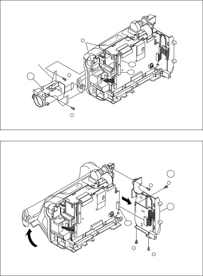
|
(L |
2 ) |
BRACKET (OP) |
|
|
ASSY |
|
4a |
|
|
|
|
16 |
4b |
4 |
(S 4 ) |
|
17 (S 4 )
Fig. 1-3-4
NOTE 5
19
18 (S 5 ) (S 5 )
5
5a
20
(S 5 )
 21 (S 5 )
Fig. 1-3-5
1-5

|
6 |
|
|
|
|
|
|
|
27 |
|
|
|
|
|
|
|
|
(S |
7 ) |
|
|
|
|
|
|
|
|
(L |
6 a) |
|
|
|
|
6a |
|
|
|
|
|
|
|
|
||
NOTE |
7 |
|
|
|
|
|
|
|
|
|
|
|
|
|
|
|
24 |
|
|
|
|
|
|
|
(S |
6 b) |
|
|
(L |
6 b) |
|
|
|
|
|
|
|
|
(S |
23 |
6b |
|
|
|
|
7 |
|
6 b) |
|
|
|
|
|
|
|
|
|
|
|
|
|
|
|
|
|
|
|
|
25 |
|
26 |
|
6c |
|
|
|
|
(S |
6 c) |
|
|
|
|
|
(S |
6 c) |
|||
|
|
|
|
|
22 |
|
|
|
|
|
|
|
(S |
6 a) |
|
|
|
|
|
Fig. 1-3-6 |
|
|
|
|
|
|
|
|
|
8 |
|
|
|
8b |
|
|
8c |
|
|
|
29 |
8a |
|
|
(S 8 ) |
|
|
|
|
|
NOTE 8 |
|
a |
|
8d |
|
|
|
EJECT SW |
28 |
||
|
|
|
|
NOTE |
8 |
b |
(S 8 ) |
|
|
|
Fig. 1-3-7 |
10 |
|
|
30 |
|
|
|
(S |
9 a) |
|
|
|
||
|
SHIELD |
|
|
|
|
|
(L 9 c) |
PLATE |
|
|
|
|
|
|
|
|
(L |
9 a) |
|
|
|
|
|
9a |
|
9 |
|
|
|
|
|
|
|
9c |
9b |
|
|
|
|
|
|
|
|
|
|
|
|
32 |
|
|
|
|
|
(S |
9 b) |
|
|
|
(L |
9 b) |
|
|
|
|
31 |
|
|
|
|
|
(S |
9 b) |
|
|
|
|
Fig. 1-3-8 |
|
|
|
|
|
|
1-6
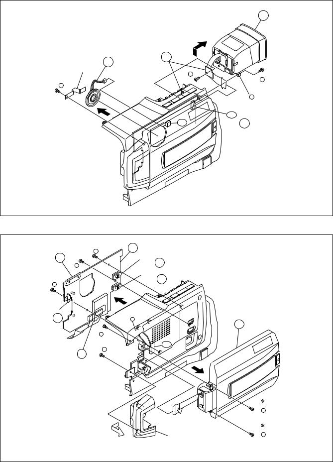
11
|
NOTE 11 b |
|
PLATE |
12 |
|
(SPK) |
33 |
|
|
(S 11 a) |
34 |
35 |
|
(S 11 b) |
(S 12 ) |
|
|
|
|
(L 11 ) |
|
|
11a |
|
12a |
NOTE 11 a |
|
Fig. 1-3-9 |
|
40 |
14 |
|
(S 14 ) |
|
|
NOTE 14 b |
SW |
|
41 |
NOTE 14 d |
|
(S 14 ) |
||
|
||
|
SW |
|
42 |
NOTE 14 c |
|
(S 14 ) |
|
|
SW |
|
|
NOTE 13 |
(L 14 ) |
|
|
13 |
|
36 |
|
|
(S 13 a) |
||
37 |
13a |
|
(S 13 |
a) |
|
NOTE 14 a |
|
|
|
38 |
|
|
(S 13 |
b) |
|
39 |
|
COVER |
(S 13 |
b) |
(HINGE) |
|
|
 : 0.147N·m (1.5kgf·cm)
Fig. 1-3-10
1-7
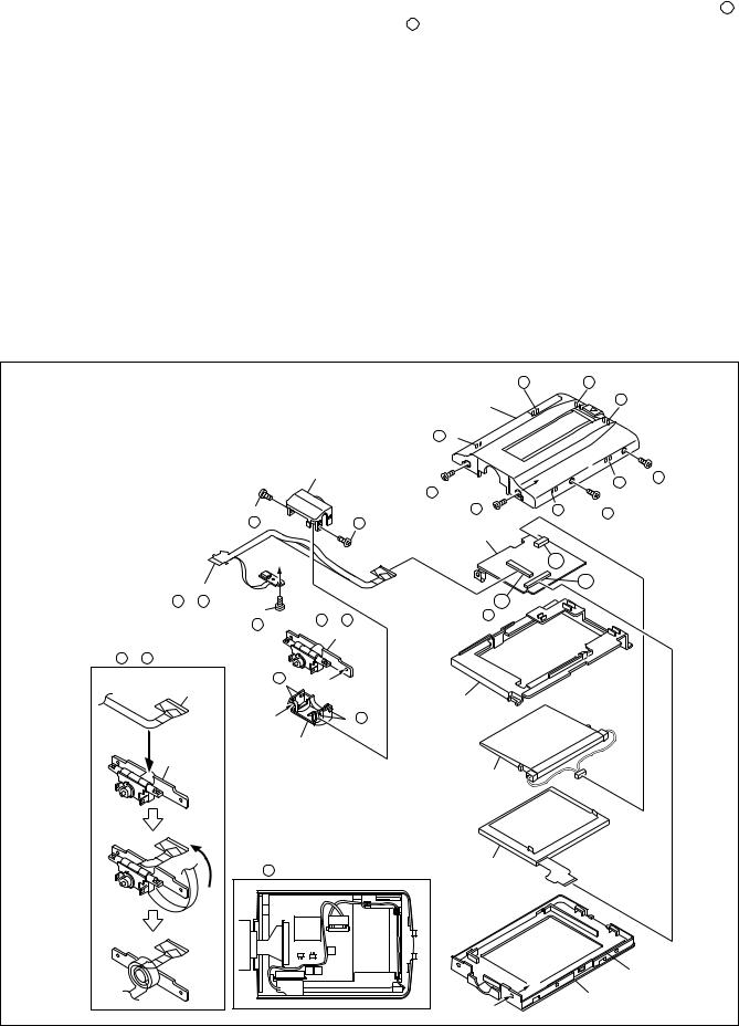
1.4 # MONITOR ASSEMBLY
Note: The shape of the monitor assembly varies by the size of the LCD screen.
For the 2.5”-type LCD, refer to Fig. 1-4-1.
1.4.1Disassembly/assembly of monitor assembly (for 2.5”-type LCD)
Note: Be careful not to soil or scratch the monitor screen through the disassembly/assembly work.
1.Remove the four screws 1 to 4 in numerical order. While disengaging the six hooks (L#a to L#f) in alphabetical order, remove the monitor cover assembly.
2.Unlock the connector a and then disconnect the FPC while lifting the hinge assembly upwards to remove it together with the FPC.
Note#a: For disconnecting the FPC, unlock the connector first and then lift the hinge assembly upwards. Accordingly, the FPC is disconnected together with the hinge assembly.
Note#b: Treat the wires carefully.
3.Unplug the wires and FPCs from the two connectors b , c , and then remove the MONITOR BL board assembly, holder (PWB) and backlight in that order.
4.Remove the LCD module.
1.4.2Disassembly/assembly of hinge assembly (for 2.5”-type LCD)
1.Remove the three screws (5 to 7), and then remove the hinge covers (1) and (2) by disengaging a total of four hooks (L#g, L#h) at the two sides.
2.Separate the SW board assembly and the FPC from the hinge assembly.
Note#c: When connecting the FPC, arrange the FPC wire by winding it around the shaft (hinge pin) of the hinge assembly by two and a half turns while paying heed to the orientation of the hinge assembly and FPC.
Note#d: When disassembling/assembling the hinge assembly, pay careful attention to every part not to damage anything.
* |
: 0.069N·m (0.7kgf·cm) |
|
|
|
(L 13 c) |
(L13 f) |
|
||
|
|
Monitor cover |
|
|
(L 13 e) |
|
|||
** : 0.098N·m (1.0kgf·cm) |
|
|
|
|
|
||||
|
|
|
assy |
|
|
|
|||
|
|
|
|
|
|
|
|||
|
|
|
|
(L 13 b) |
|
|
|
|
|
|
Hinge |
cover(1) |
|
|
a |
|
|
2* |
|
|
3** |
|
|
(L 13 d) |
(S 13 a) |
||||
|
|
|
|
|
|
||||
|
|
|
|
(S 13 b) |
4** |
|
|
1* |
|
|
|
|
|
|
|
|
|
||
|
6* |
|
7* |
|
(S 13 b) |
(L 13 a) |
|
|
|
|
|
|
(S 13 a) |
|
|||||
|
(S 13 d) |
|
(S 13 d) |
LCD BL PWB |
|
|
|
|
|
|
|
|
|
|
|
|
|
||
|
c |
|
|
|
|
b |
|
|
|
|
MONI. FPC ASSY |
|
|
|
|
|
c |
|
|
|
|
|
|
a |
|
|
|
|
|
|
Note 13 c / 13 d |
|
|
|
|
|
|
|
|
|
5* |
Note 13 c / 13 d |
|
Note 13 a |
|
|
|
|
|
|
(S 13 c) |
|
|
|
|
|
|
||
|
|
Hinge assy |
|
|
|
|
|
|
|
|
|
|
|
|
|
|
|
|
|
|
Note 13 c / 13 d |
|
|
|
|
|
|
|
|
|
(L 13 g) |
b |
|
|
|
|
|
|
|
|
FPC |
|
|
Holder |
|
|
|
|
|
|
|
|
|
|
|
|
|
||
|
c |
|
(L 13 h) |
(PWB) |
|
|
|
|
|
|
|
|
|
|
|
|
|
||
|
Hinge |
cover(2) |
|
|
|
|
|
|
|
|
Hinge |
|
|
|
|
|
|
|
|
|
|
|
|
|
Back light |
|
|
|
|
|
Note 13 b |
|
|
|
LCD module |
|
|
|
|
|
|
|
|
|
|
|
|
|
|
|
|
|
|
|
b |
|
|
Bracket(Earth) |
|
|
|
|
|
|
|
|
|
|
|
|
|
|
|
|
a |
Monitor |
case assy |
||
|
|
|
|
|
|
|
|
|
|
|
|
|
Fig. 1-4-1 |
|
|
|
|
|
|
1-8
Loading...