


GP1S73P
Compact Photointerrupter
GP1S73P/GP1S74P
with Connector
GP1S73P/GP1S74P
■■
1. Compact type
2. Snap-in mounting type
3. 3 kinds of mounting plate thickness
(Applicable plate thickness : 1.0, 1.2 and 1.6 mm)
■
Applications
1. Copiers
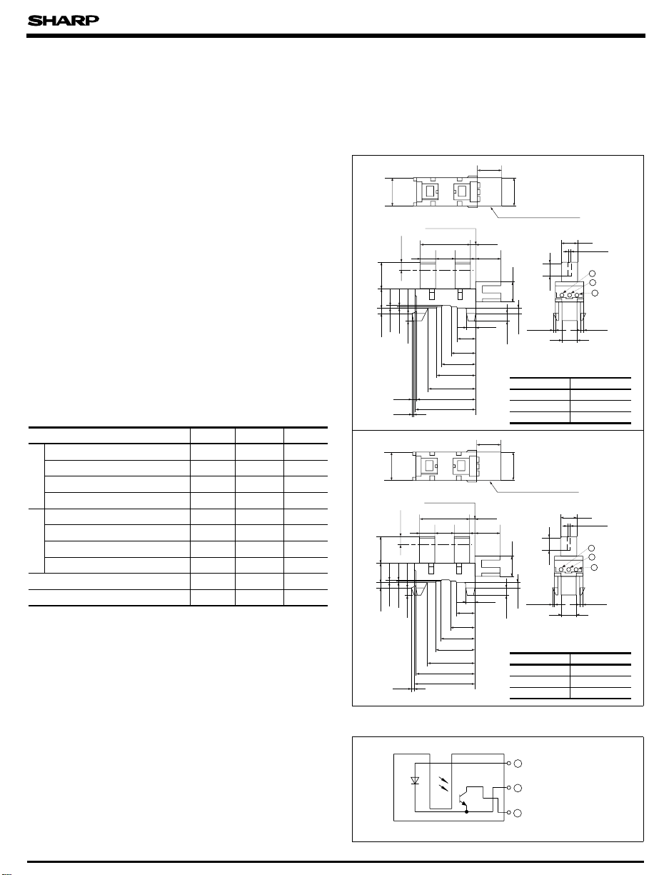
Outline DimensionsFeatures
GP1S73P
8.0
7.25.61.1
)
2.3
(
(Sensor center)
JAPAN
(Case surface)
13.6
5.0
4.3 4.3
(Unit : mm)
( 6.8 )
73
SHARP
6.8±1
( 7.8 )
JAPAN AMP made
connector 175487-3
1.6
)
5.8
(
4.7
2-0.5 ± 0.1
(Slit)
3.2
1 Collector
2 GND
3 Anode
2. Laser beam printers
3. Facsimiles
■
Absolute Maximum Ratings
Forward current
*1
Peak forward current
InputOutput
Reverse voltage
Power dissipation
Collector-emitter voltage
Emitter-collector voltage
Collector current
Collector power dissipation
Operating temperature
Storage temperature
*1 Pulse width 100µ s, Duty ratio=0.01
*2 The connector should be plugged in/out at normal temperature.
I
F
I
FM
V
R
P75mW
V
CEO
V
ECO
I
C
P
C
T
opr
T
stg
(Ta=25˚C)
Rating UnitParameter Symbol
50 mA
1A
6V
35 V
6V
20 mA
75 mW
- 25 to + 85
- 40 to + 85
˚C
˚C
0.6
0.75
GP1S74P
8.0
7.25.61.1
0.6
0.7
0.2
2.3
( 2.3 )
(Sensor center)
0.2
2.3
14.0
16.81.2
17.0
JAPAN
(Case surface)
13.6
5.0
4.3 4.3
14.0
16.8
17.0
2.4
5.4
6.9
9.9
11.4
74
5.4
6.9
9.9
11.4
1.1
2.3
* Unspecified tolerances shall be
as follows.
*
( ) : Connector dimensions for reference
Tolerance Dimension(d)
± 0.15
± 0.2
± 0.3
( 6.8 )
( 7.8 )
SHARP
6.8± 1
JAPAN AMP made
connector 175487-3
1.6
( 5.8 )
2.4
1.1
2.3
* Unspecified tolerances shall be
as follows.
*
( ) : Connector dimensions for reference
Tolerance Dimension(d)
± 0.15
± 0.2
± 0.3
3.2
4.0
5.0<= d < 15.0
15.0 <= d
4.7
2-0.5 ± 0.1
(Slit)
1 Collector
4.0
5.0<= d < 15.0
15.0 <= d
2-0.92-0.5
d < 5.0
2 GND
3 Anode
2-0.92-0.5
d < 5.0
■
Internal Connection Diagram (Both GP1S73P/GP1S74P)
3 Anode
2 GND
1 Collector
Electro-optical Characteristics
■
Parameter Symbol MIN. TYP. MAX. UnitConditions
Forward voltage
Input
Peak forward voltage
Reverse current
Output
Dark current
Collector current
Transfer
characteristics
Collector-emitter saturation voltage
Response time
Rise time
Fall time
V
F
V
FM
I
R
I
CEO
I
C
V
CE(sat
t
r
t
f
= 20mA
I
F
I
FM
V
R
V
CE
V
CE
)
= 40mA, IC= 0.5mA
I
F
V
CE
R
L
=0.5A
=3V
= 20V
= 5V, IF= 20mA
= 2V, IC= 2mA
= 100 Ω
GP1S73P/GP1S74P
(Ta=25˚C)
- 1.2 1.4 V
-V
3.0 4.0
--10µA
- 1 100 nA
0.5 - 15 mA
-- V
-315µs
-420µs
0.4
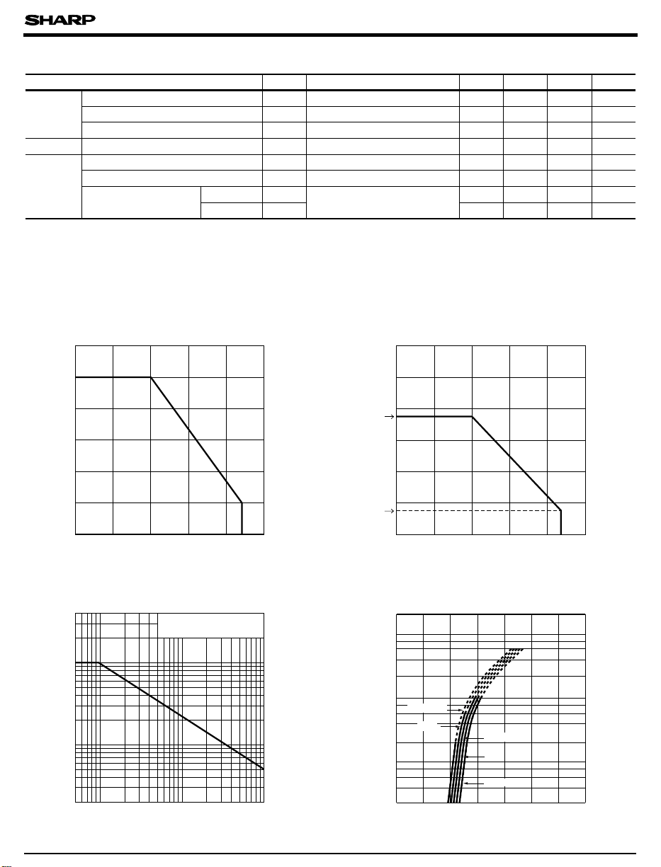
Fig. 1 Forward Current vs. Ambient
Temperature
60
50
)
mA
40
(
F
30
20
Forward current I
10
0
- 25 0 25 50 100
75 85
Fig. 2 Collector Power Dissipation vs.
Ambient Temperature
)
100
mW
(
C
80
75
60
40
20
15
Collector power dissipation P
0
- 25 0 25 50 75 100
85
Ambient temperature Ta (˚C) Ambient temperature Ta (˚C)
Fig. 3 Peak Forward Current vs. Duty Ratio Fig. 4 Forward Current vs. Forward Voltage
Pulse width<= 100µs
= 25˚C
T
2000
1000
(mA)
FM
500
200
100
50
Peak forward current I
20
-2
55252
10
a
-1
10
Duty ratio
1
1000
500
200
)
mA
100
(
F
50
Ta= 85˚C
20
50˚C
10
Forward current I
5
2
1
0 0.5 1.0 1.5 2.0 2.5 3.0 3.5
25˚C
0˚C
- 25˚C
Forward voltage VF (V
)
 Loading...