


GP1S50/GP1S51V/GP1S52V/GP1S54
GP1S50/GP1S51V
GP1S52V/GP1S54
■ Features
1.High sensing accuracy ( Slilt width : 0.5mm )
2.Both-sides mounting type : GP1S50 (Case height : 10mm ) Either-side mounting type : GP1S51V (Case height : 10mm ) PWB direct mounting type : GP1S52V (Case height : 10mm ) PWB direct mounting type : GP1S54 (Case height : 8mm )
■ Outline Dimensions
GP1S50 |
19.0 |
± |
0.2 |
|
|
|
|
|
|
|
|
|
|
|
|
|
|
|
|
|
|
|
|
|
5.0 |
6.0 |
|
|
|
|
2 - φ 3.2 ± 0.2 |
2 - C2.0 |
|
|
|
||||
|
25.0 ± 0.3 |
|
|
Slit width |
(Both sides of |
||||
|
12.2 ± 0.3 |
|
|
||||||
|
+ 0.2 |
|
|
|
0.5 |
detector and |
|||
|
3.0 - 0.1 |
|
|
|
|
emitter ) |
|||
3.5 |
|
|
1.5 |
7.5 |
10.0 |
|
7.0 |
|
|
|
|
|
|
|
|
MIN. |
|
|
|
4 - 0.4 -+ |
0.10.3 |
|
|
|
|
10.0 |
4 - 0.45 -+ 0.10.3 |
||
|
|
|
|
|
|||||
|
(9.2) |
|
|
|
(2.54) |
|
|||
|
2 |
|
3 |
|
|
|
|
|
|
|
|
|
|
|
|
* Unspecified tolerances shall be as follows; |
|||
|
|
|
|
|
|
Dimensions(d) Tolerance |
|||
|
1 |
|
4 |
|
|
|
d<= 6.0 |
± 0.1 |
|
Marking : GP1S50 |
|
|
|
|
6.0< d<= 18.0 |
± 0.2 |
|||
|
|
|
|
18.0< d<= 25.0 |
± 0.25 |
||||
|
|
|
|
|
|
* ( ) : |
Reference dimensions |
||
GP1S52V |
12.2 + 0.3 |
|
|
|
|
|
|
|
|
|
- 0.3 |
|
|
|
|
|
|
|
|
|
3 +- 0.10.2 |
|
|
|
|
|
|
|
|
S52 |
|
|
5 |
(Both sides of |
5.0 |
|
|||
|
|
|
detector and |
|
|||||
|
|
|
|
|
|
||||
|
12.2± |
0.3 |
|
emitter ) |
0.5 |
|
C1.0 |
||
1.5 |
3.0+ 0.2 |
3.5 |
|
Slit width |
|
|
|||
- |
0.1 |
|
|
|
|
|
|||
|
|
|
|
|
|
|
|||
2.5 7.5 |
|
|
|
|
MIN. 10.0 |
|
|
4 |
+ 0.3 |
4 - 0.4 -+ |
0.10.3 |
|
|
|
10.0 |
|
|
- 0.45 - 0.1 |
|
|
|
|
|
|
|
|
|||
|
|
|
|
|
|
|
|
||
|
(9.2) |
|
|
|
|
(2.54) |
|||
|
|
|
|
|
|
|
|||
4 |
|
|
|
1 |
|
* Unspecified tolerances shall be as follows; |
|||
|
|
|
|
|
|
Dimensions(d) Tolerance |
|||
|
|
|
|
|
|
|
d<=6.0 |
± 0.1 |
|
3 |
|
|
|
2 |
|
6.0< d<=18.0 |
± 0.2 |
||
|
|
|
|
|
|
|
|
||
* ( ) : Reference dimensions
General Purpose
Photointerrupter
■ Applications
1.OA equipment, such as FDDs, printers, facsimiles
2.VCRs
|
|
|
|
|
|
|
(Unit : mm ) |
||
GP1S51V |
2.0 |
|
|
|
|
|
|
|
|
5 |
S51 |
|
|
|
|
|
|
|
|
|
|
3 -+ |
0.10.2 |
|
|
|
|
|
|
|
12.2 -+ 0.30.3 |
|
|
|
|
(Both sides of |
|||
|
12.2 ± 0.3 |
|
|
|
|
|
detector and |
||
|
+ 0.2 |
|
|
|
|
5.0 |
emitter ) |
|
|
1.5 |
3.0 - 0.1 |
|
3.5 |
|
|
0.5 |
|
2 - |
φ 3.2 ± 0.2 |
|
|
|
|
Slit width |
|||||
|
|
|
|
7.5 |
7.0 |
|
6.0 |
10.0 |
|
4 - 0.4 -+ |
0.10.3 |
|
MIN. |
2.5 |
|
|
4 - 0.45-+ |
0.10.3 |
|
|
10.0 |
|
|
|
|||||
|
|
|
|
|
|
|
|
|
|
|
|
|
|
|
|
(2.54) |
|
|
|
|
(9.2) |
|
|
|
|
12.0 |
|
|
|
4 |
|
1 |
|
|
|
18.0 |
|
|
|
|
|
|
* Unspecified tolerances shall be as follows ; |
||||||
|
|
|
|
|
|||||
|
|
|
|
|
Dimensions(d) Tolerance |
|
|||
3 |
|
2 |
|
|
|
d<= 6.0 |
± 0.1 |
|
|
|
|
|
6.0< d<= 18.0 |
± 0.2 |
|
||||
|
|
|
|
|
|
||||
|
|
|
|
|
* ( ) : |
Reference dimensions |
|||
GP1S54 |
|
|
|
|
|
|
|
|
|
|
center |
12.2 ± 0.3 |
( |
Detector |
3.0+- 00.4 |
) |
|
|
2.5 |
|
|
0.7 6.0 |
|
GP1S54 |
- |
|
|
2
4 - 0.4+- 0.30.1
(9.2)
7.5± 0.1
(Both sides of detector and emitter ) 0.5
Slit width
12.0MIN. 8.0
5.0
C1.0
2 - R0.3MAX.
4 - 0.45 +- 0.30.1
(2.54)
4.2 |
|
|
1 |
* Unspecified tolerances shall be as follows; |
|||
|
|
Dimensions(d) Tolerance |
|||||
|
|
2 |
|||||
|
|
|
|
d<=6.0 |
± 0.1 |
||
|
|
2 |
- φ 0.7 |
|
|||
4 |
3 |
6.0< d<=18.0 |
± 0.2 |
||||
1.75 |
|||||||
* ( ) : |
Reference dimensions |
||||||
|
|
||||||
|
|
|
|
||||
“ In the absence of confirmation by device specification sheets, SHARP takes no responsibility for any defects that occur in equipment using any of SHARP's devices, shown in catalogs, data books, etc. Contact SHARP in order to obtain the latest version of the device specification sheets before using any SHARP's device”.
GP1S50/GP1S51V/GP1S52V/GP1S54
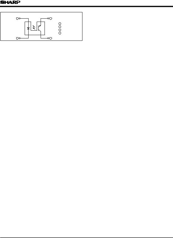
Internal connection diagram (Common to 4 models )
1 |
4 |
1 |
Anode |
2 |
Cathode |
3Collector
4Emitter
2 |
3 |
■ Absolute Maximum Ratings |
|
|
(Ta = 25˚C ) |
||
|
|
|
|
|
|
|
Parameter |
Symbol |
Rating |
|
Unit |
|
Forward current |
IF |
50 |
|
mA |
Input |
*1 Peak forward current |
I FM |
1 |
|
A |
Reverse voltage |
V R |
6 |
|
V |
|
|
|
||||
|
Power dissipation |
P |
75 |
|
mW |
|
Collector-emitter voltage |
VCEO |
35 |
|
V |
Output |
Emitter-collector voltage |
VECO |
6 |
|
V |
Collector current |
IC |
20 |
|
mA |
|
|
|
||||
|
Collector power dissipation |
P C |
75 |
|
mW |
|
Operating temperature |
T opr |
- 25 to + 85 |
|
˚C |
|
Storage temperature |
Tstg |
- 40 to + 100 |
|
˚C |
|
*2 Soldering temperature |
Tsol |
260 |
|
˚C |
*1 Pulse width<=100μ s, Duty ratio= 0.01 |
|
|
|
|
|
*2 For 5 seconds |
|
|
|
|
|
■ Electro-optical Characteristics |
|
|
|
|
(Ta = 25˚C ) |
|||||
|
|
|
|
|
|
|
|
|
|
|
|
Parameter |
|
Symbol |
Conditions |
MIN. |
TYP. |
MAX. |
Unit |
||
|
Forward |
|
GP1S50/ GP1S51V/ GP1S52V |
VF |
IF = 20mA |
- |
1.25 |
1.4 |
V |
|
Input |
voltage |
|
GP1S54 |
- |
1.2 |
1.4 |
||||
|
|
|
|
|||||||
Peak forward voltage |
VFM |
IFM = 0.5A |
- |
3 |
4 |
V |
||||
|
||||||||||
|
Reverse current |
I R |
VR = 3V |
- |
- |
10 |
μ A |
|||
Output |
Collector dark current |
ICEO |
VCE = 20V |
- |
1 |
100 |
nA |
|||
Transfer |
Collector Current |
Ic |
IF = 20mA, VCE = 5V |
0.5 |
- |
5 |
mA |
|||
charac- |
Collector-emitter saturation voltage |
VCE ( sat ) |
IF = 40mA, I C = 0.5mA |
- |
- |
0.4 |
V |
|||
teristics |
Response time |
|
Rise time |
t R |
VCE = 2V, I CE = 2mA |
- |
3 |
15 |
μ s |
|
|
|
Fall time |
t F |
RL = 100 Ω |
- |
4 |
20 |
μ s |
||
|
|
|
||||||||
 Loading...