


GP1A53HR
GP1A50HR/GP1A51HR/GP1A52HR/GP1A53HR
GP1A50HR/GP1A51HR
GP1A52HR/GP1A53HR
OPIC
Photointerrupter
■ Features
1. High sensing accuracy
(
Slit width : 0.5mm
)
2. LSTTL and TTL compatible output
■ Applications
1. OA equipment, such as printers, facsimiles,
2. VCRs
etc.
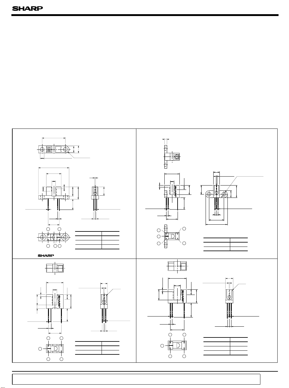
■ Outline Dimensions
(
Unit : mm
)
0.5
(
9.2
)
(
1.27
)
2 - C2.0
6.0
5.0
1.5
7.5
10.0
7.0
3.5
GP1A50HR
GP1A52HR GP1A53HR
A53
S
A52
S
GP1A51HR
1.5
3.5
(
9.2
)
(
1.27
)
0.5
Slit width
10.0
5.0
C1.0
7.52.5
C1.0
0.5
5.2
(
1.27
)
10.0
7.5
1.5
(
10.3
)
1A51HR
1A50HR
3.5
1.5
7.5
(
9.2
)
Slit width
0.5
2 -
(
1.27
)
5.0
7.0
12.0
18.0
6.0
10.0
2.0
(
1.27
)
(
1.5
)
(
1.5
)
(
1.27
)
(
1.5
)
3.5
(
1.5
)
(
1.27
)
145
32
Marking :
Slit width
(
Both sides of
emitter and
detector
)
*Unspecified tolerances shall be as follows:
Dimensions
(
d
)
Tolerance
d<=6.0 ± 0.1
6.0< d<=18.0 ± 0.2
18.0< d<=25.0 ±0.025
*
(
)
: Reference dimensions
5
4
3
1
2
(
Both sides of
emitter and
detector
)
Dimensions
(
d
)
Tolerance
d<=6.0 ± 0.1
6.0< d<=18.0 ± 0.2
*Unspecified tolerances shall be as follows :
*
(
)
: Reference dimensions
1A52HR
23
15
4
(
Both sides
of emitter
and detector
)
*Unspecified tolerances shall be as follows:
*
(
)
: Reference dimensions
Dimensions
(
d
)
Tolerance
d<=6.0 ± 0.1
6.0< d<=18.0 ± 0.2
Slit width
(
Both sides
of emitter
and detector
)
1A53HR
15
4
32
*Unspecified tolerances shall be as follows:
Dimensions
(
d
)
Tolerance
d<=6.0 ± 0.1
6.0< d<=18.0 ± 0.2
18.0< d<=25.0 ± 0.25
*
(
)
: Reference dimensions
Both-sides mounting type : GP1A50HR
(
Gap: 3mm
)
Either-side mounting type : GP1A51HR
(
Gap: 3mm
)
PWB mounting type : GP1A52HR
(
Gap: 3mm
)
3.
An OPIC consists of a light-detecting element and signal-
processing circuit integrated onto a single chip.
*“OPIC”
(
Optical IC
)
is a trademark of the SHARP Corporation.
data books, etc. Contact SHARP in order to obtain the latest version of the device specification sheets before using any SHARP's device.”
“ In the absence of confirmation by device specification sheets, SHARP takes no responsibility for any defects that occur in equipment using any of SHARP's devices, shown in catalogs,
19.0
±
0.2
2
-
φ 3.2
± 0.2
25.0
±
0.3
12.2
±
0.3
3.0
+ 0.2
-
0.1
9.0
MIN.
5
-
0.4
+
0.3
-
0.1
5 - 0.45
+0.3
- 0.1
5
-
0.4
+
0.3
-
0.1
5 - 0.45
+ 0.3
- 0.1
3.0
+
0.2
-
0.1
2-
φ
3.2
±
0.2
12.2
±
0.3
9.0
MIN.
13.7
±
0.3
10.0
MIN.
5
-
0.4
+ 0.3
-
0.1
5 - 0.45
+ 0.3
- 0.1
5.0
+ 0.2
-
0.1
5
-
0.45
+ 0.3
-
0.1
5 - 0.4
+
0.3
-
0.1
3.0
+ 0.2
-
0.1
12.2
±
0.3
9.0
MIN.
GP1A53HR
(
Gap: 5mm
)
GP1A50HR/GP1A51HR/GP1A52HR/GP1A53HR
■ Absolute Maximum Ratings
(
Ta= 25˚C
)
*1 Pulse width<=100µs, Duty ratio= 0.01
*2 For 5 seconds
■ Electro-optical Characteristics
(
Ta = 25˚C
)
*5 GP1A53HR Condition of V
OH
, I
CCH
, Response time; I
F
= 8mA
Parameter Symbol Rating Unit
Input
Forward current I
F
50 mA
*1
Peak forward current I
FM
1A
Reverse voltage V
R
6V
Power dissipation P 75 mW
Output
Operating temperature
Supply voltage V
CC
- 0.5 to + 17 V
Output current I
O
50 mA
Power dissipation P
O
250 mW
T
opr
- 25 to + 85 ˚C
Storage temperature T
stg
- 40 to + 100 ˚C
*2
Soldering temperature T
sol
260 ˚C
*3 I
FLH
represents forward current when output changes from low to high.
*4 I
FHL
represents forward current when output changes from high to low. Hysteresis stands for I
FHL
/I
FLH.
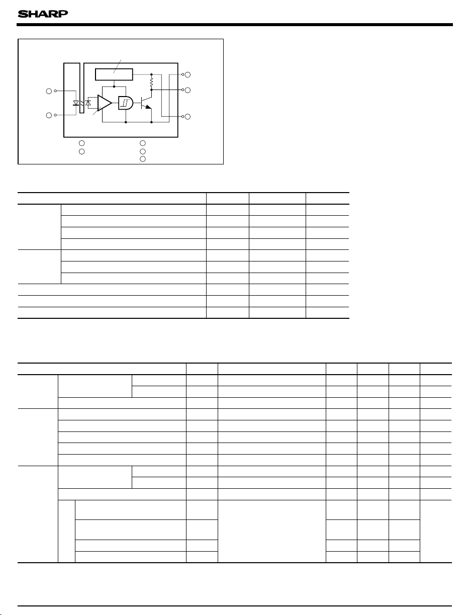
Internal connection diagram
Voltage regulator
Amp
1
2
3
4
5
1 Anode
2 Cathode
3 V
CC
4 V
O
5 GND
Parameter Symbol Conditions MIN. TYP. MAX. Unit
Input
Output
Transfer
charac-
teristics
Forward voltage
GP1A52HR
V
F
I
F
= 5mA - 1.1 1.4 V
GP1A53HR
V
F
I
F
= 8mA - 1.14 1.4 V
Reverse current I
R
V
R
= 3V - - 10.0 µ A
V
CC
4.5 - 17.0 V
Low level output voltage V
OL
V
CC
= 5V, I
F
= 0, I
OL
= 16mA - 0.15 0.4 V
High level output voltage V
OH
4.9 - - V
Low level supply current I
CCL
V
CC
= 5V, I
F
= 0 - 1.7 3.8 mA
High level supply current I
CCH
- 0.7 2.2 mA
*3
“Low→High”
threshold input current
GP1A52HR
I
FLH
V
CC
= 5V - 1.0 5.0 mA
GP1A53HR
I
FLH
V
CC
= 5V - 1.5 8.0 mA
*4
Hysteresis
I
FHL
/I
FLH
V
CC
= 5V 0.55 0.75 0.95
“Low→High”
propagation delay time
t
PLH
R
L
= 280Ω
3.0 9.0
µ s
-
-
5.0 15.0
“High→Low”
propagation delay time
t
PHL
- 0.1 0.5
time
Response
Rise time t
r
- 0.05 0.5Fall time t
r
GP1A50HR/GP1A51HR
Operating supply voltage
GP1A50HR/GP1A51HR
V
CC
= 5V,
*5
I
F
= 5mA
V
CC
= 5V,
*5
I
F
= 5mA
V
CC
= 5V,
*5
I
F
= 5mA
(
15kΩ
)
 Loading...