


CTC 175176

CTC175/176/177/186/187
Supplemental Training Manual
VERTICAL
TO
E8
RED BIAS
<21-B>
TO
E7
GRN BIAS
E5003
E5007
TP50
RED OUTP UT
194V
THO MSO N TECHNIC AL TRAINING
This training manual is a supplement to the CTC175/176/177 technical training manual (T-CTC175/
6/7-1). It contains additional information regarding system control circuit changes in later production
CTC175/76/77 chassis, new CTC186/87 circuits and an in-depth description of the tuner-onboard circuitry with troubleshooting strategies. This publication also contains "Tech Tips" from the
field on commonly encountered problems and their solutions. Using this manual in conjunction with
the CTC175/176/177 technical training manual and service data will enable the field technician to
repair these chassis more effectively and efficiently.
FOREWORD
Note: This publication is intended to be used only as a training aid. It is not intended to replace service
data. Thomson Consumer Electronics Service Data for these instruments contains specific
information about parts, safety and alignment procedures and must be consulted before performing
any service. The information in this publication is as accurate as possible at the time of publication.
Circuit designs and drawings are subject to change without notice.
SAFETY INFORMATION CAUTION
Safety information is contained in the appropriate Thomson Consumer Electronics Service Data. All
product safety requirements must be compiled with prior to returning the instrument to the consumer.
Servicers who defeat safety features or fail to perform safety checks may be liable for any resulting
damages and may expose themselves and others to possible injury.
All integrated circuits, all surface mounted devices, and many other semiconductors are electrostatically sensitive and therefore require special handling
techniques.
Prepared by
Thomson Consumer Electronics, Inc.
Technical Training Department
10330 North Meridian Street, Indianapolis, Indiana 46290-1024
U.S.A.

Table of Contents
CTC186/87 .................................................................................... 1
System Control .............................................................................. 4
MicroProcessoer Pinout .......................................................................................5
Comb Filter.................................................................................... 6
Troubleshooting .................................................................................................................................6
Stereo Decoder ..............................................................................7
dbx Alignments ..................................................................................................................................8
Inductor /Capacitor (LC) Basics .................................................... 14
Varactor Diode ................................................................................................................................15
Basic Tuner....................................................................................16
Oscillator / Mixer / IF Bandpass........................................................................................................ 17
PLL / Frequency Synthesizer............................................................................................................. 17
CTC176/77/86/87 Tuner ................................................................ 18
Single Tuned Filter ........................................................................................................................... 21
RF Amplifier.................................................................................................................................... 23
Double Tuned Filter.......................................................................................................................... 23
OSC., Mixer, PLL ...........................................................................................................................26
IF Amp ........................................................................................................................................... 29
Tuner Alignment ............................................................................................................................... 30
Troubleshooting ...............................................................................................................................31
Tuner Voltage Charts........................................................................................................................ 33
Tech Tips ..................................................................................... 41
Page 3
The CTC186/87 chassis is virtually the same as the CTC176/77 with the addition of a
dbx Stereo Decoder / Comb filter board. For complete descriptions of the common
circuitry, refer to the CTC175/176/177 Technical Training Manual (publication number
T-CTC175/6/7/-1).
CTC186/87
Later production CTC175/176/177 chassis have a different microprocessor (U3101).
These chassis can be identified with a “2” after the alpha suffix on the bar code label.
For example, a CTC177AA chassis that had the new version microprocessor would be
labeled CTC177AA2. This is extremely important because the pinouts are not the same.
In other words, they are NOT interchangeable. The CTC186/87 also supports this
newer version microprocessor.
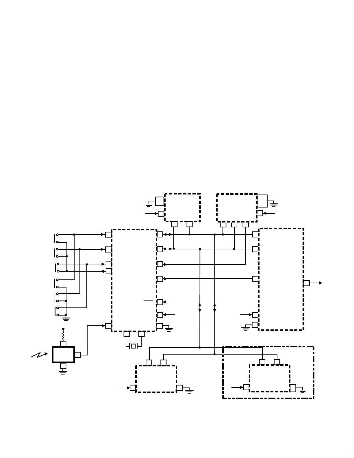
The use of the bus controlled stereo decoder (U1600) and the new Thomson ST-9
microprocessor (U3101), changes the system control block diagram slightly to accommodate the different parts. The differences are pin-out changes on the microprocessor
and the addition of U1600, figure 1. With the exception of these changes, the system
control circuit is functionally the same as the CTC177 (see the System Control section
of the CTC177 training manual).
POWER
VOL. UP
VOL. DN.
CH. UP
1,2, 3
GND
U3201
4,7
5V
KS1
6
KS2
7
KS3
8
KD1
5
T-CHIP DATA
TUNER CLOCK
T-CHIP CLOCK
TUNER DATA
U3101
µ
P
PIP
ENABLE
T-CHIP
ENABLE
8
19
20
12
14
EEPROM
VDD
DATA
5
CLO CK
6
DATA
20 21
U2901
D-PIP
CLOC K
GND
VDD
ENABLE
22
39
54
53
52
System Control
3,5
15, 16
40, 41
5V
DATA
CLOCK
U1001
T-CHIP
ENABLE
HORZ.
OUT
24
CH. DN.
MENU
5V
2
IR3401
3
5V
2
RESET
VDD
21
OSC
OSC
GND 56
1
OUT
36 37
1
Y3101
22
IN
4
DATA
CLOCK
5V
5
U7401
5V
TUNER PLL
VCC
10
GND
13
7.6 V
STBY
9V
CTC186/87 ONLY
22
STEREO DEC OD ER
VCC
15
BUS
GND
1
DATA
U1600
2
CLOC K
GND
3,4,
17
Figure 1, System Control Block Diagram
Page 4
U3101 - Thomson ST-9 SYSTEM CONTROL MICROPROCESSOR
PIN NO. NAME VOLTAGE
1 IR IN 4.5
2 RESET 5
3 NC 4 DEGAUSS 0
5 KD1 0
6 KS1 4.7
7 KS2 4.7
8 KS3 4.7
9 DATA OUT 0.3
10 ATE ENABLE 0
11 CC VIDEO 2
12 PIP ENABLE 4.7 >20M
13 NC -
14 T-CHIP ENBL 4.6 >20M
15 BLUE OSD 0
16 GRN OSD 0
17 RED OSD 0
18 FSW 0
19
20
T-CHIP DATA
TUNER/ST CLK
T-CHIP CLK
TUNER/ST DATA
4.5
4.7 >200K Serial communication - data/clock
21 VDD 4.7
22 VSS 0
23 PLL FILTER 2.6
24 PLL BIAS 2.2
25 PLL VCC 4.7
26 H 0.7
27 V 0.2
28
EXP S T SW
ST / MONO
11 / 0 36K Expanded stereo, NWS-gain and mono /stereo control line.
29 SPK MUTE 0
30 TONE 0 / 5
31
SCLOCK/FM
ON/OFF
0 >20M
32 ST SENSE 0 / 5
33 RF SEC * VARIES >20M
34 RF PRI * VARIES >20M
35 SINGLE TUN * VARIES
36 OSC OUT 2.3
37 OSC IN 2.3
38 TUN SYNC 2.3 >20M
39 FM TUN * VARIES
40 IF DEFEAT 0
41 STBY SW 42 DATA IN 4.8
IN CKT. RES.
>300K
>200K
>20M
>20M
>200K
>200K
>200K
>20M
10K
>50K
-
1K
1K
1K
2K
>20M
>20M
0
>20M
6K
>20M
8K
1.8K
>100K
>100K
>20M
>20M
>20M
>20M
>20M
>20M
>20M
>200K
Serial communication line used to control data between
the micro. and PIP.
Serial comm. line used to control communication between
the micro and T-Chip.
Fast switch - controls OSD and video switching in T-chip.
Serial clock for DBX stereo decoder. FM on control for
commercial TV.
PWM output - Controls the secondary of the double tuned
filter in the tuner.
PWM output - Controls the primary of the double tuned
filter in the tuner.
PWM output - Controls the single tuned filter in the tuner.
Sync input to detect the presence of an active channel
when tuning.
Input to detect an active FM station on commercial TV.
Page 5
DESCRIPTION
IR input signal from remote control.
Micro reset - active LO.
-
Activates degaussing relay.
Keyboard drive line.
Keyboard scan input.
Keyboard scan input.
Keyboard scan input.
Data out for commercial television.
Used for factory testing.
Closed caption video input.
-
Blue OSD output.
Green OSD output.
Red OSD output.
Serial communication - data/clock.
Power supply input for microprocessor.
Ground for microprocessor.
PLL filter network.
PLL bias resistor Connection.
Power supply for PLL.
Horizontal timing input for OSD.
Vertical timing input for OSD.
Goes HI to mute speakers.
Goes HI for low tone and LO for high tone.
Stereo Detect line for non-DBX stereo sets.
8MHz crystal connection.
8MHz crystal connection.
Output to defeat IF circuit via AGC.
-
Data input for commercial television.
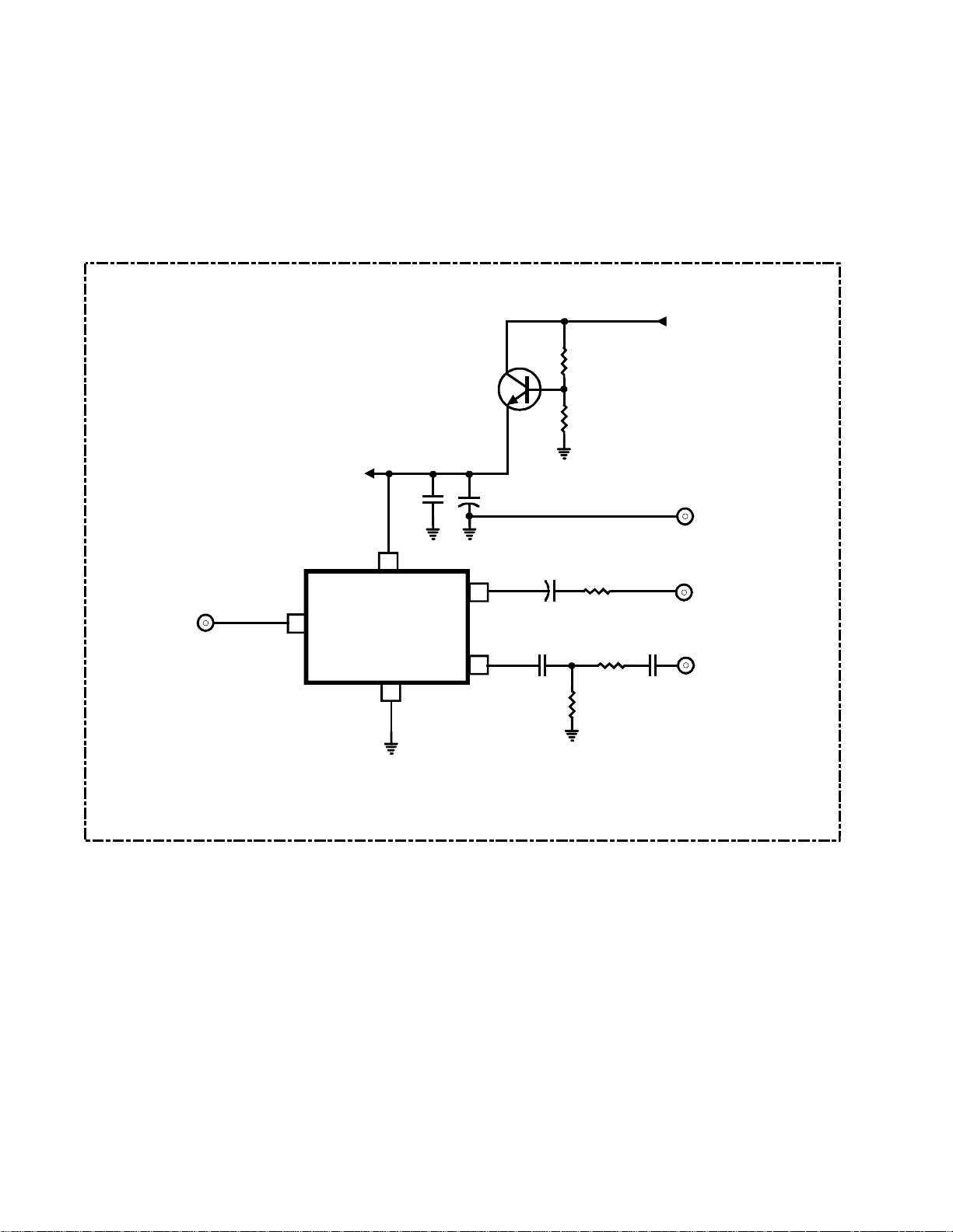
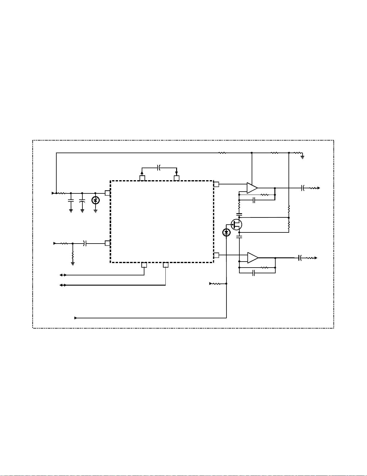
This board contains an analog comb filter that is used to separate luminance and chrominance. Composite video is routed from the main board from E2601 and applied to the
input at pin 2 of the comb filter IC (FL2651). Luma is output at pin 5 and chroma is
output at pin 3. These signals are sent back to the main board at E2602 and E2603
where they are input to the T-Chip (U1001), figure 2. Refer to the luminance and
chrominance processing section of the CTC177 training manual for signal processing on
the main board.
+12V
Q2651
+9V
+
Comb Filter
E2505
GND
1
5
E2601
VIDEO IN
2
FL2651
3
4
STEREO DECODER / COMB FILTER PCB
Figure 2, Comb Filter
1. Check for composite video at E2601. If there is no video present, the problem is on
the main board and not the comb filter. If video is present, go to the next step.
2. Check for luma and chroma out at E2602 and E2603. If luma and chroma are
present, the comb filter is working correctly. If they are not present, go to the next
step.
E260 2
LUM A OUT
E260 3
CHROMA OU T
Troubleshooting
3. Check for 9 volts at pin 1 of the comb filter (FL2651). If the voltage is present,
suspect a defective FL2651. If the voltage is missing, check Q2651 and its associated components.
Page 6
Stereo Decoder
The stereo decoder (U1600) receives wideband audio from the main board and decodes left and right audio information. Wideband audio enters the board at JS107
(figure 3) and is capacitively coupled to U1600 pin 11. Decoded left and right signals
are output at pins 29 and 28 respectively. U1601 buffers the left and right output and
provides the expanded stereo feature in conjunction with Q1601. When the expanded
stereo line (JS112) goes LO, Q1601 turns on and cross-mixes the left and right channel
information to produce a perceived increase in stereo separation. Pins 1 and 7 of U1601
output the left and right signals respectively that are capacitively coupled back to the
main board via JS105 and JS106.
+12V
JS103
WBA
JS107
SCLK
JS111
SDATA
JS110
EXP. STEREO
JS112
+
CR1600
9.1V
+
15
11
VCC
WBA IN
8 7
MAIN
OUT
MAIN
IN
U1600
STEREO DECODER
2 1
STEREO DECODER / COMB FILTER PCB
L OUT
R OUT
+12V
29
CR1601
28
U1601
3
2
Q1601
U1601
5
6
8
+
1
-
+
7
-
+
+
LEFT
JS105
RIGHT
JS106
Figure 3, DBX Stereo Decoder
Page 7
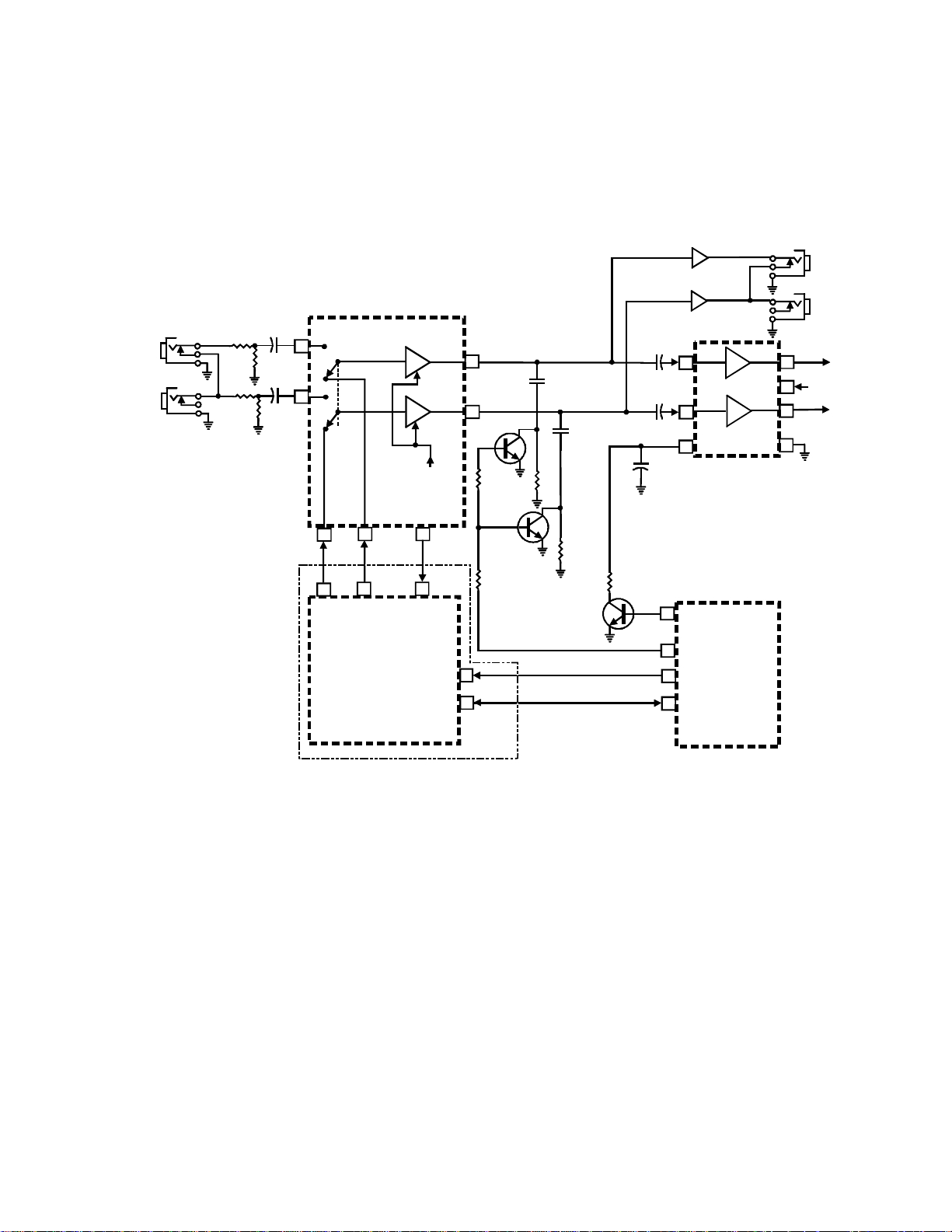
U1600 is digitally controlled over the I2C bus. Analog lines that were used in the
CTC177 for stereo sense and stereo select (see the Audio Processing section of the
CTC177 training manual) are no longer used. Instead, communications between U1600
and the television’s microprocessor are carried out over the serial bus, figure 4.
U1001
T-CHIP
AMP
AMP
BUS
CTL
VOL ./M UTE
BUS CTL
WB AUDIO
OUT
L INR IN
4
5
3
60
C1912
59
Q1901
C1913
R1912
Q1902
+
5
+
1
+
3
AUX LEFT
AUDIO INPUT
AUX RIGHT
AUDIO INPUT
+
7
+
8
AMP
AMP
U1901
8
9
10
6
LEFT HI-FI
OUT
R / MO NO
HI-FI
OUT
LEFT
26V
RIGHT
Q1903
MUTE
R1913
29
30
20
19
29
28
R OUT
TV
AUDIO
L OUT
11
WB AUDIO
IN
U1600
ST EREO
DECODE R
STEREO DECODER / COMBFILTER PCB
SCLK
SDATA
1
2
Figure 4, Audio Circuit Block Diagram
The CXA 1734S Stereo/SAP Mpx IC registers are accessed via the IIC Bus. All
necessary bus controls are contained in the SERVICE MENU.
Signal Description Summary
ALIGNMENT INPUT SIGNAL DESCRIPTIONMEASUREMENT
WBA Input;JS107
#25 ATT 100 Hz, 424 mv rms JS106 (RIGHT OUT)
#26 STVCO Open WBA or short AC to gnd. JS106 (RIGHT OUT)
#27 SAPVCO 78,670 Hz (5 x fH), 255 mv rms Observe OSD * (star)
#28 STLPF 9.4 KHz, 1.04 v rms Observe OSD STEREO”
#29 SAPBPF 88 KHz, 206 mv rms Observe OSD * (star)
#30 WBSEP Stereo, LEFT only, 300 Hz w/ pilotJS106 (RIGHT OUT)
#31 SPECSEP Stereo, LEFT only, 3KHz, w/ pilot JS106 (RIGHT OUT)
SPEAKR
MUTE
TONE
SCLK
SDATA
U310 1
SYSCON
dbx Alignments
Page 8

NOTES:
• All replacement stereo IC’s must be aligned according to this procedure.
• All Stereo/SAP alignments must be performed in the sequence shown. Several
alignments are coarse alignments for ones that follow.
• When the set starts up, the dbx Stereo IC will be aligned with IIC alignment data
which is stored in EEPROM memory from the previous IC that was installed in the
set. In most cases, stereo and SAP will be detected, but the stereo and SAP vco
free-running frequencies will not be properly aligned. Neither will stereo separation
nor the various internal filters be optimized. The full alignment procedure must be
performed to make sure the IC performs within specification.
• A modulator or other signal source with video must be connected to the tuner, and
the set tuned to the appropriate channel in order to detect stereo. Stereo and SAP
alignments cannot be performed with VIDEO IN selected (channel 00).
Alignment Preparation
Make sure that the EXPANDED STEREO function is turned off, otherwise the output
amplitudes will be in error. Also, STEREO SEPARATION alignments will be impossible.
Access the SERVICE MENU for the dbx IC as follows:
1. Press and hold the MENU button, then while holding MENU press the ON button,
followed by the VOLUME + button. This accesses the GENERAL SERVICE
MENU display.
2. Release all buttons.
3. Increment VALUE (V) number to 76 by pressing and holding the VOLUME UP
button.
4. Increment PARAMETER (P) number to 13 by pressing and holding the CHANNEL
UP button.
5. Increment V number to 77 with VOLUME UP button.
6. Increment P number to 25 with CHANNEL UP button. This is the first alignment
parameter.
Page 9

Perform the alignments in the following sequence.
Attenuator (ATT = Parameter # 25)
DAC range = 0 to 15.
All following alignments depend on the correct setting of this alignment.
1. Unsolder and lift the bottom end of R1609 from the circuit board. This is the
Wideband Audio input (WBA) to the CXA1734 stereo IC.
2. Connect an audio generator to the unsoldered end of R609 (WBA). Adjust the
generator output for 100 Hz, 424 mv rms, +/- 10 mv at module pin #7, WBA. This
corresponds to a full 25KHz carrier deviation mono audio signal from the sound IF.
3. Connect an AC voltmeter to module JS106, RIGHT CHANNEL OUTPUT. This is
also the bottom end of R612. (Do not use the top end, or oscillations may result.)
Adjust the ATT DAC using the volume control button. Set the DAC for an output
level as close to 489 mv rms as possible. Each DAC step will change the output
level by about 25 mv.
4. Observe on an oscilloscope that the audio output at module pins #5 (LEFT) and #6
(RIGHT) are clean and undistorted.
5. Observe that the rms amplitude of both pins #5 and #6 are within 20 mvrms of each
other.
6. If the final DAC alignment value is not within the range of 7 - 11, check to make
sure that the signal amplitude is proper. (Do not use 1KHz, because the internal deemphasis filter will cause an amplitude error.)
STEREO VCO free running frequency. (STVCO = Parameter # 26)
DAC range = 0 to 63.
This alignment is also a course adjustment for the next alignment.
1. Remove the audio generator connection from the bottom end of R1609. False
STVCO frequency will be generated if WBA is not open, as VCO tries to lock to
noise or other frequency.
2. Connect a frequency counter to module JS106, RIGHT OUT. (4 x fH vco is
automatically routed to JS106 when in P#26.)
3. Adjust DAC while monitoring frequency. Set DAC for frequency = 62,936 Hz +/200Hz. (4 x fH). The frequency increment for each DAC step is approximately 300
Hz.
Page 10

SAPVCO free running frequency. (SAPVCO = Parameter # 27)
DAC range = 0 to 15.
This is not a direct frequency measurement. It uses the internal status registers of
the stereo IC to indicate PLL lock. The previous alignment (STVCO) is a coarse
adjust for this alignment.
1. Adjust audio generator for 78.67 KHz, 254 mv rms (559 Vp-p), +/- 10 mv. (5 x
fH SAP subcarrier, equivalent to 15 KHz carrier deviation) at WBA input.
2. Set SAPVCO DAC to step # 0. Observe TV screen. No star (*) should be
present.
3. Increment DAC once per second or slower until * becomes present. Record this
DAC setting. (A flashing * is OK. Usually, one more DAC increment will stop the
flashing.)
4. Set DAC to step # 15. Observe that no * is present. Decrement DAC until * once
again becomes present. Record this DAC setting.
5. Average the DAC settings from steps (c) and (d). Set DAC to this averaged value.
This is the proper alignment value for SAPVCO. Setting will usually be 1 - 14. If
not, verify that previous step was done properly.
STEREO LOWPASS FILTER (STLPF = Parameter # 28)
DAC range = 0 to 63.
This alignment is also a course adjustment for the next alignment.
1. Adjust audio generator for 9.4 KHz, 1.04 vrms (1.47 Vp-p) at WBA input.
2. Set STLPF DAC to step # 0. Observe TV screen. No “STEREO” indicator
should be present.
3. Increment DAC once per second or slower until “STEREO” indicator becomes
present. Record this DAC setting. (It is OK for the “STEREO” indicator to flash.
Usually, one more DAC increment will stop the flashing.)
4. Set DAC to step # 63. Observe that no “STEREO” indicator is present. Decrement DAC until “STEREO” indicator once again becomes present. Record this
DAC setting.
5. Average the DAC settings from steps (c) and (d). Set DAC to this averaged value.
This is the proper alignment value for STLPF.
Page 11

SAP BANDPASS FILTER (SAPBPF = Parameter # 29)
DAC range = 0 to 15.
1. Adjust audio generator for 88 KHz, 220 mv rms, +/- 10 mv.
2. Set SAPBPF DAC to step # 0. Observe TV screen. No * should be present.
3. Increment DAC once per second or slower until * becomes present. Record this
DAC setting.
4. Set DAC to step # 15. Observe that no * is present. Decrement DAC until * once
again becomes present. Record this DAC setting.
5. Average the DAC settings from steps (c) and (d). Set DAC to this averaged value.
This is the proper alignment value for SAPBPF.
WIDEBAND SEPARATION (WBSEP = Parameter # 30)
DAC range = 0 to 63.
This alignment is for the dbx WIDEBAND detector
1. Set stereo generator for STEREO LEFT CHANNEL ONLY SIGNAL, 300 Hz.
2. Connect AC rms voltmeter to module JS106, RIGHT CHANNEL OUT.
3. Set WBSEP DAC to step # 31 (DAC midpoint).
4. Start incrementing WBSEP DAC (or decrementing, as necessary) while observing
voltmeter reading. Find DAC setting which produces a minimum voltmeter reading
(null setting). Record this DAC setting. The exact null setting will typically be
difficult to determine, because the null range is rather broad.
5. Measure module JS105, LEFT CHANNEL OUT, and check for at least 20 dB
separation between LEFT and RIGHT.
6. This alignment will be repeated after doing the next alignment, because of some
interaction between the WBSEP and SPECSEP DAC’s.
Page 12

SPECTRAL SEPARATION (SPECSEP = Parameter # 31)
DAC range = 0 to 63.
This alignment is for the dbx SPECTRAL detector
1. Set stereo generator for STEREO LEFT CHANNEL ONLY SIGNAL, 3KHz.
Note:If the MTS generator being used is not capable of generating a 3KHz signal,
the alignment cannot be performed. If this is the case, set the DAC to the nominal
default of 35.
2. Connect AC rms voltmeter to module JS106, RIGHT CHANNEL OUT.
3. Set SPECSEP DAC to step # 31 (DAC midpoint).
4. Start incrementing SPECSEP DAC (or decrementing, as necessary) while observing
voltmeter reading. Find DAC setting which produces a minimum voltmeter reading
(null setting). Record this DAC setting. The exact null setting will typically be
difficult to determine, because the null range is rather broad. Do the best you can.
5. Measure module JS105, LEFT CHANNEL OUT, and check for at least 20 dB
separation between LEFT and RIGHT.
Page 13
A television tuner receives (or selectively tunes) a 6MHz bandwidth RF (Radio Fre-
N
quency) carrier that contains audio and video information and converts it to a common IF
signal (Intermediate Frequency). The IF signal is demodulated by the television into its
audio and video components. All tuners work on the principle of a tuned circuit whose
resonant frequency determines what channel is tuned. By changing the tuned circuits’
resonant frequency, different RF carriers (channels) are selected. Before discussing the
different sections that comprise the tuner’s circuitry, it is appropriate to review certain
fundamental concepts of inductors, capacitors and varactors. These components play a
major role in all tuned circuits.
Inductors
Remember, an inductor is simply a coil of wire. The ability of a coil to oppose a change
in current is a measure of the inductance L of the coil. Inductance is measured in henries
(H). For inductors in series, the total inductance is found in the same manner as resistors
in series, figure 5. Likewise, the total inductance of inductors in parallel is found in the
same manner as resistors in parallel, figure 5. The main idea to remember here is inductors added in parallel reduce the total inductance and inductors added in series in-
crease the total inductance.
Inductor /
Capacitor
(LC) Basics
1
T
L
L
T
L
2
L
3
L
LT = L1+L2+L3+- -- -L
1
L
2
L
N
3 L
L
N
L
N
Figure 5, Inductors in Series and Parallel
Capacitors
Capacitors are components that are made up of two parallel conducting plates separated
by an insulating material. A capacitor stores a charge on its plates. The storage capacity
C is measured in Farads (F). The farad is generally too large a unit for most tuner
applications so the pico farad (pF) 10
-12
F is used. Total capacitance is calculated in
the opposite manner as inductance, figure 6. Capacitors in parallel increase total
capacitance and capacitors in series decrease total capacitance.
C T
C
1
C
C
2
3
C
N
1 1 1 1 1
= + + + − − −
1 2 3
T
C C C C C
T
C
C
1
CT = C1+ C2+ C3+ --- - C
C
2
N
C
3
N
C
Figure 6, Capacitors in Series and Parallel
Page 14
 Loading...