


Q529.1E-LA
Table of contents
 Loading...
Colour Television Chassis
VE8
ME8+
Q529.1E
LA
ME8+
VE8
Contents Page Contents Page
1. Technical Specifications, Connections, and Chassis
Overview 2
2. Safety Instructions, Warnings, and Notes 6
3. Directions for Use 7
4. Mechanical Instructions 8
5. Service Modes, Error Codes, and Fault Finding 14
6. Block Diagrams, Test Point Overview, and
Waveforms
Wiring Diagram 32" (ME8) 45
Wiring Diagram 32" (VE8) 46
Wiring Diagram 37" (ME8) 47
Wiring Diagram 42" + 47" (ME8) 48
Wiring Diagram 42" (VE8) 49
Wiring Diagram 47" (VE8) 50
Wiring Diagram 52" (VE8) 51
Block Diagram Video 52
Block Diagram Audio 53
Block Diagram Control & Clock Signals 54
Block Diagram Main Display Supply (42") 55
SSB: Test Points (Top Side) 56
SSB: Test Points (Bottom Side) 57
I2C IC Overview 58
Supply Lines Overview 59
7. Circuit Diagrams and PWB Layouts Drawing PWB
Main Power Supply IPB 42": Stby, MF (A1) 60 63-64
Main Power Supply IPB 42": HV Inverter (A2) 61 63-64
Main Power Supply IPB 42": DC / DC (A3)62 63-64
4 LED Back UPEC Panel: LED Drive (AL1)65 68
4 LED Back UPEC Panel: DC / DC (AL2) 66 68
4 LED Back UPEC Panel: uC Block (AL3) 67 68
6 LED Back UPEC Panel: LED Drive (AL1)69 72
6 LED Back UPEC Panel: DC / DC (AL2) 70 72
6 LED Back UPEC Panel: uC Block (AL3) 71 72
8 LED Back UPEC Panel: LED Drive (AL1)73 77
©
Copyright 2008 Koninklijke Philips Electronics N.V.
All rights reserved. No part of this publication may be reproduced, stored in a
retrieval system or transmitted, in any form or by any means, electronic,
mechanical, photocopying, or otherwise without the prior permission of Philips.
8 LED Back UPEC Panel: DC / DC (AL2) 74 77
8 LED Back UPEC Panel: uC Block (AL3) 75 77
8 LED Back UPEC Panel: LED Drive (AL4)76 77
4 LED Lite-On Panel: LED Drive (AL1) 78 81
4 LED Lite-On Panel: DC / DC (AL2) 79 81
4 LED Lite-On Panel: uC Block (AL3) 80 81
4 LED MD OPAMP Lite-on (32") (AL1) 82 84
4 LED MD OPAMP Lite-on (32") (AL2) 83 84
6 LED MD OPAMP Lite-on (42") (AL1) 85 87
6 LED MD OPAMP Lite-on (42") (AL2) 86 87
6 LED Lite-On Panel: LED Drive (AL1) 88 91
6 LED Lite-On Panel: DC / DC (AL2) 89 91
6 LED Lite-On Panel: uC Block (AL3) 90 91
8 LED Lite-On Panel: LED Drive (AL1) 92 96
8 LED Lite-On Panel: DC / DC (AL2) 93 96
8 LED Lite-On Panel: uC Block (AL3) 94 96
8 LED Lite-On Panel: LED Drive (AL4) 95 96
Small Signal Board (6214.4 version) (B01-B10) 97-150 154-163
SSB: SRP List Explanation 151
SSB: SRP List Part 1 152
SSB: SRP List Part 2 153
Small Signal Board (6214.6 version) (B01-B10)164-216 221-230
SSB: SRP List Explanation 217
SSB: SRP List Part 1 218
SSB: SRP List Part 2 219
SSB: SRP List Part 3 220
AmbiLight Interface Panel (FA) 231 231
IR & LED Panel (VE) (J) 232 233
Light Guide Panel (L) 236 237
8. Alignments 243
9. IC Data Sheets 261
10. Spare Parts List & CTN Overview 274
11. Revision List 274
I_17661_000.eps
140408
Published by EL 0870 BU TV Consumer Care Printed in the Netherlands Subject to modification EN 3122 785 17666

EN 2 Q529.1E LA1.
Technical Specifications, Connections, and Chassis Overview
1. Technical Specifications, Connections, and Chassis Overview
Index of this chapter:
1.1 Technical Specifications
1.2 Connections
1.3 Chassis Overview
Notes:
• Figures can deviate due to the different set executions.
• Specifications are indicative (subject to change).
1.1 Technical Specifications
1.1.1 Vision
Display type : LCD
Screen size : 32" (82 cm), 16:9
: 37" (94 cm), 16:9
: 42" (107 cm), 16:9
: 47" (120 cm), 16:9
Resolution (H × V pixels) : 1920 × 1080
Min. light output (cd/m
Min. contrast ratio : 55000:1
Max. response time (ms) : 2, 3, 5, 6 (depending
Viewing angle (H × V degrees) : 176 × 176
Tuning system : PLL
TV Colour systems : PAL B/G, D/K, I
Video playback : NTSC
Tuner bands : UHF, VHF, S, Hyper
Supported video formats
- 60 Hz : 480i
- 60 Hz : 480p
- 50 Hz : 576i
- 50 Hz : 576p
- 50/60 Hz : 720p
- 50/60 Hz : 1080i
- 24/25/30/50/60 Hz : 1080p
Supported computer formats:
- 60 Hz : 640 × 480
- 60 Hz : 800 × 600
- 60 Hz : 1024 × 768
- 60 Hz : 1280 × 768
- 60 Hz : 1360 × 768
- 60 Hz : 1920 × 1080i
- 60 Hz : 1920 × 1080p
Presets/channels : 100/125 presets
Tuner bands : VHF
2
) : 500
: 52" (132 cm), 16:9
: 1366 × 768
: 450 (52")
(32PFL9603D/10 and
52")
: 33000:1
(32PFL7623D/10)
: 30000:1 (37", 42" and
47")
on display)
: SECAM B/G, D/K, L/L’
: DVB-T COFDM 2K/
8K, MPEG4 (optional)
: PAL
: SECAM
: UHF
: S-band
: Hyper-band
: BBE
Maximum power (W
1.1.3 Multimedia
Supported formats : Slideshow.alb files
USB input : USB1.1 (12 Mbps)
Network : DLNA PC Network
1.1.4 Miscellaneous
Power supply:
- Mains voltage (V
- Mains frequency (Hz) : 50 / 60
Ambient conditions:
- Temperature range (°C) : +5 to +35
Power consumption (values are indicative)
- Normal operation (W)
- 32" : ≈139/140
- 37" : ≈186
- 42" : ≈110/248
- 47" : ≈155/305
- 52" : ≈243
- Standby (W) : < 0.15
Dimensions (W × H × D in mm)
- 32" : 828 × 543 × 109
- 37" : 953 × 604 × 101
- 42" : 1054 × 658 × 100
- 47" : 1170 × 736 × 125
- 52" : 1300 × 803 × 128
Weight (kg)
- 32" : 16.3
- 37" : 19.2
- 42" : 22.7
- 47" : 35.0
- 52" : 40.6
):2 × 15
RMS
: MPEG1
: MPEG2
:MP3
: JPEG
: USB2.0 (480 Mbps)
link
) : 220 - 240 ±10%
AC
: 90% R.H.
1.1.2 Sound
Sound systems : FM-stereo B/G
: NICAM B/G, D/K, I, L
: AV Stereo
: Virtual Dolby Digital
Technical Specifications, Connections, and Chassis Overview
EN 3Q529.1E LA 1.
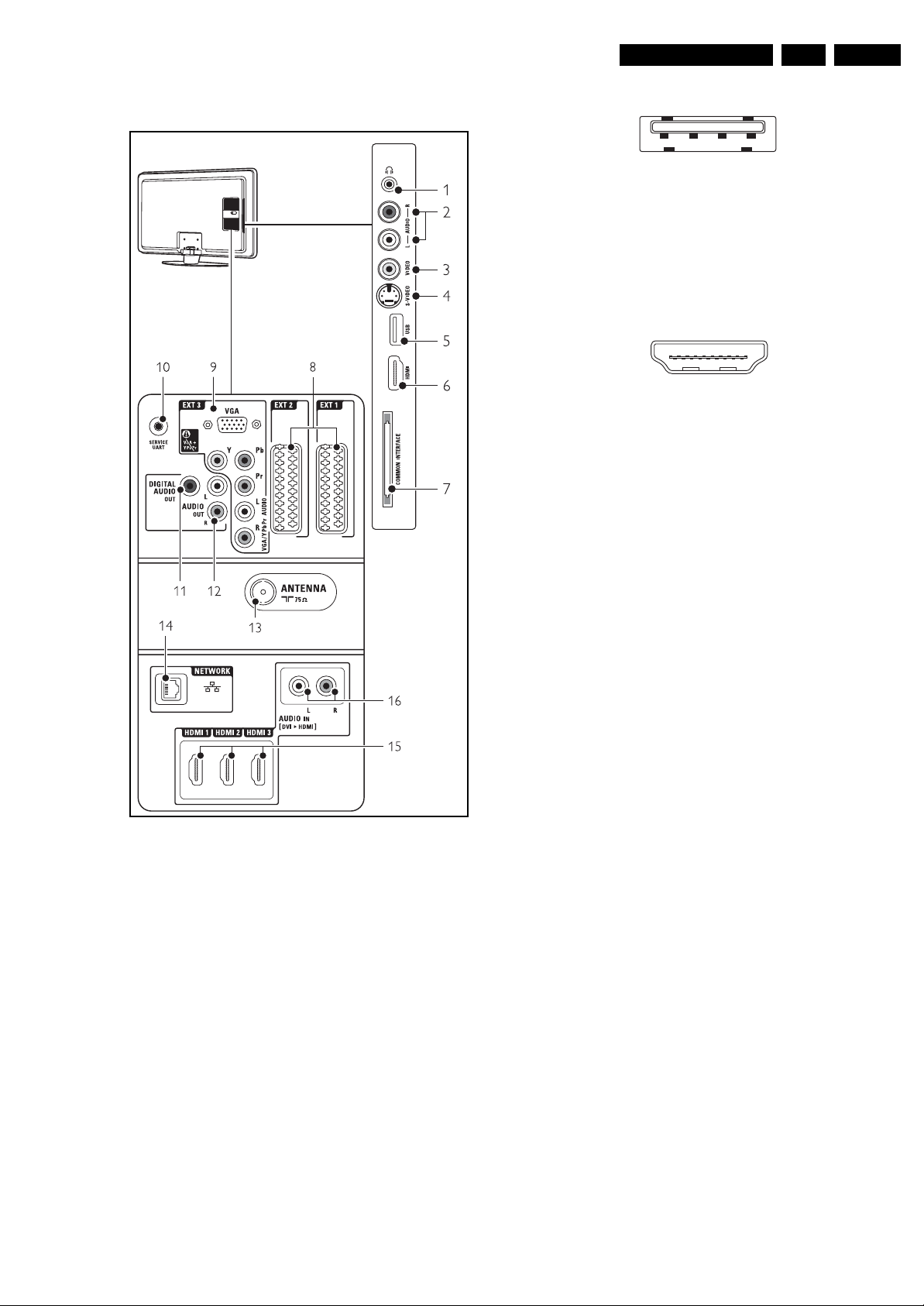
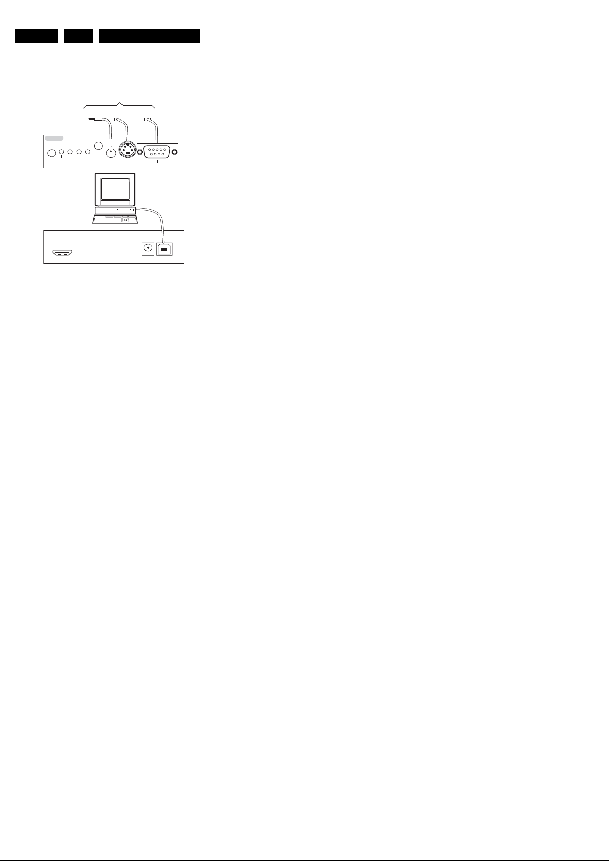
1.2 Connections
5 - USB2.0
1 2 3 4
E_06532_022.eps
300904
Figure 1-2 USB (type A)
1-+5V k
2 -Data (-) jk
3 -Data (+) jk
4 -Ground Gnd H
6 - HDMI: Digital Video, Digital Audio - In
19
18 2
1
E_06532_017.eps
250505
Figure 1-3 HDMI (type A) connector
1 -D2+ Data channel j
2-Shield Gnd H
3 -D2- Data channel j
4 -D1+ Data channel j
5-Shield Gnd H
6 -D1- Data channel j
7 -D0+ Data channel j
8-Shield Gnd H
9 -D0- Data channel j
10 - CLK+ Data channel j
11 - Shield Gnd H
12 - CLK- Data channel j
13 - n.c.
14 - n.c.
15 - DDC_SCL DDC clock j
16 - DDC_SDA DDC data jk
17 - Ground Gnd H
18 - +5V j
19 - HPD Hot Plug Detect j
20 - Ground Gnd H
Figure 1-1 Connection overview
Note: The following connector colour abbreviations are used
(acc. to DIN/IEC 757): Bk= Black, Bu= Blue, Gn= Green,
Gy= Grey, Rd= Red, Wh= White, Ye= Yellow.
1.2.1 Side Connections
1 - Headphone (Output)
Bk - Headphone 32 - 600 Ω / 10 mW ot
2 - Cinch: Audio - In
Rd - Audio R 0.5 V
Wh - Audio L 0.5 V
/ 10 kΩ jq
RMS
/ 10 kΩ jq
RMS
3 - Cinch: Video CVBS - In
Ye - Video CVBS 1 V
/ 75 Ω jq
PP
4 - S-Video (Hosiden): Video Y/C - In
1 -Ground Y Gnd H
2 -Ground C Gnd H
3 -Video Y 1 V
4 -Video C 0.3 V
/ 75 Ω j
PP
/ 75 Ω j
PP
I_17663_001.eps
200708
7 - Common Interface
68p- See diagram B07A jk
EN 4 Q529.1E LA1.
Technical Specifications, Connections, and Chassis Overview
1.2.2 Rear Connections
8 - EXT1: Video RGB/CVBS - In, Audio - In
21
20
E_06532_001.eps
2
1
050404
Figure 1-4 SCART connector
1-n.c.
2 -Audio R 0.5 V
/ 10 kΩ j
RMS
3-n.c.
4 -Ground Audio Gnd H
5 -Ground Blue Gnd H
6 -Audio L 0.5 V
7 -Video Blue 0.7 V
8 -Function Select 0 - 2 V: INT
/ 10 kΩ j
RMS
/ 75 Ω j
PP
4.5 - 7 V: EXT 16:9
9.5 - 12 V: EXT 4:3 j
9 -Ground Green Gnd H
10 - n.c.
11 - Video Green 0.7 V
12 - n.c.
/ 75 Ω j
PP
13 - Ground Red Gnd H
14 - Ground Data Gnd H
15 - Video Red 0.7 V
/ 75 Ω j
PP
16 - Status/FBL 0 - 0.4 V: INT
1 - 3 V: EXT / 75 Ω j
17 - Ground Video Gnd H
18 - Ground FBL Gnd H
19 - n.c.
20 - Video CVBS 1 V
/ 75 Ω j
PP
21 - Shield Gnd H
8 - EXT2: Video RGB - In, CVBS - In/Out, Audio - In/Out
21 - Shield Gnd H
9 - EXT 3 VGA: Video RGB - In
1
5
6
11
10
15
E_06532_002.eps
050404
Figure 1-6 VGA Connector
1 -Video Red 0.7 V
2 -Video Green 0.7 V
3 -Video Blue 0.7 V
/ 75 Ω j
PP
/ 75 Ω j
PP
/ 75 Ω j
PP
4-n.c.
5 -Ground Gnd H
6 -Ground Red Gnd H
7 -Ground Green Gnd H
8 -Ground Blue Gnd H
9-+5V
10 - Ground Sync Gnd H
DC
+5 V j
11 - n.c.
12 - DDC_SDA DDC data j
13 - H-sync 0 - 5 V j
14 - V-sync 0 - 5 V j
15 - DDC_SCL DDC clock j
9 - EXT3: Cinch: Video YPbPr - In
Gn - Video Y 1 V
Bu - Video Pb 0.7 V
Rd - Video Pr 0.7 V
/ 75 Ω jq
PP
/ 75 Ω jq
PP
/ 75 Ω jq
PP
9 - EXT3: Cinch: Audio - In
Rd - Audio - R 0.5 V
Wh - Audio - L 0.5 V
/ 10 kΩ jq
RMS
/ 10 kΩ jq
RMS
10 - Service Connector (UART)
1 -Ground Gnd H
2 -UART_TX Transmit k
3 -UART_RX Receive j
21
20
E_06532_001.eps
2
1
050404
Figure 1-5 SCART connector
1 -Audio R 0.5 V
2 -Audio R 0.5 V
3 -Audio L 0.5 V
/ 1 kohm k
RMS
/ 10 kohm j
RMS
/ 1 kohm k
RMS
4 -Ground Audio Gnd H
5 -Ground Blue Gnd H
6 -Audio L 0.5 V
7 -Video Blue 0.7 V
8 -Function Select 0 - 2 V: INT
/ 10 kohm j
RMS
/ 75 ohm j
PP
4.5 - 7 V: EXT 16:9
9.5 - 12 V: EXT 4:3 j
9 -Ground Green Gnd H
10 - n.c
11 - Video Green 0.7 V
12 - n.c.
/ 75 ohm j
PP
13 - Ground Red Gnd H
14 - Ground P50 Gnd H
15 - Video Red 0.7 V
16 - Status/FBL 0 - 0.4 V: INT
/ 75 ohm j
PP
1 - 3 V: EXT / 75 ohm j
17 - Ground Video Gnd H
18 - Ground FBL Gnd H
19 - Video CVBS 1 V
20 - Video CVBS 1 V
/ 75 ohm k
PP
/ 75 ohm j
PP
11 - EXT3: Cinch: S/PDIF - Out
Bk - Coaxial 0.4 - 0.6V
/ 75 Ω kq
PP
12 - EXT3: Cinch: Audio - Out
Rd - Audio - R 0.5 V
Wh - Audio - L 0.5 V
/ 10 kΩ kq
RMS
/ 10 kΩ kq
RMS
13 - Aerial - In
- - IEC-type (EU) Coax, 75 Ω D
14 - RJ45: Ethernet (if present)
112345678
E_06532_025.eps
210905
Figure 1-7 Ethernet connector
1 -TD+ Transmit signal k
2 -TD- Transmit signal k
3 -RD+ Receive signal j
4-n.c.
5-n.c.
6 -RD- Receive signal j
7-n.c.
8-n.c.
Technical Specifications, Connections, and Chassis Overview
EN 5Q529.1E LA 1.
15 - HDMI 1, 2 & 3 Digital Video, Digital Audio - In
19
18 2
Figure 1-8 HDMI (type A) connector
1 -D2+ Data channel j
2-Shield Gnd H
3 -D2- Data channel j
4 -D1+ Data channel j
5-Shield Gnd H
6 -D1- Data channel j
7 -D0+ Data channel j
8-Shield Gnd H
1
E_06532_017.eps
250505
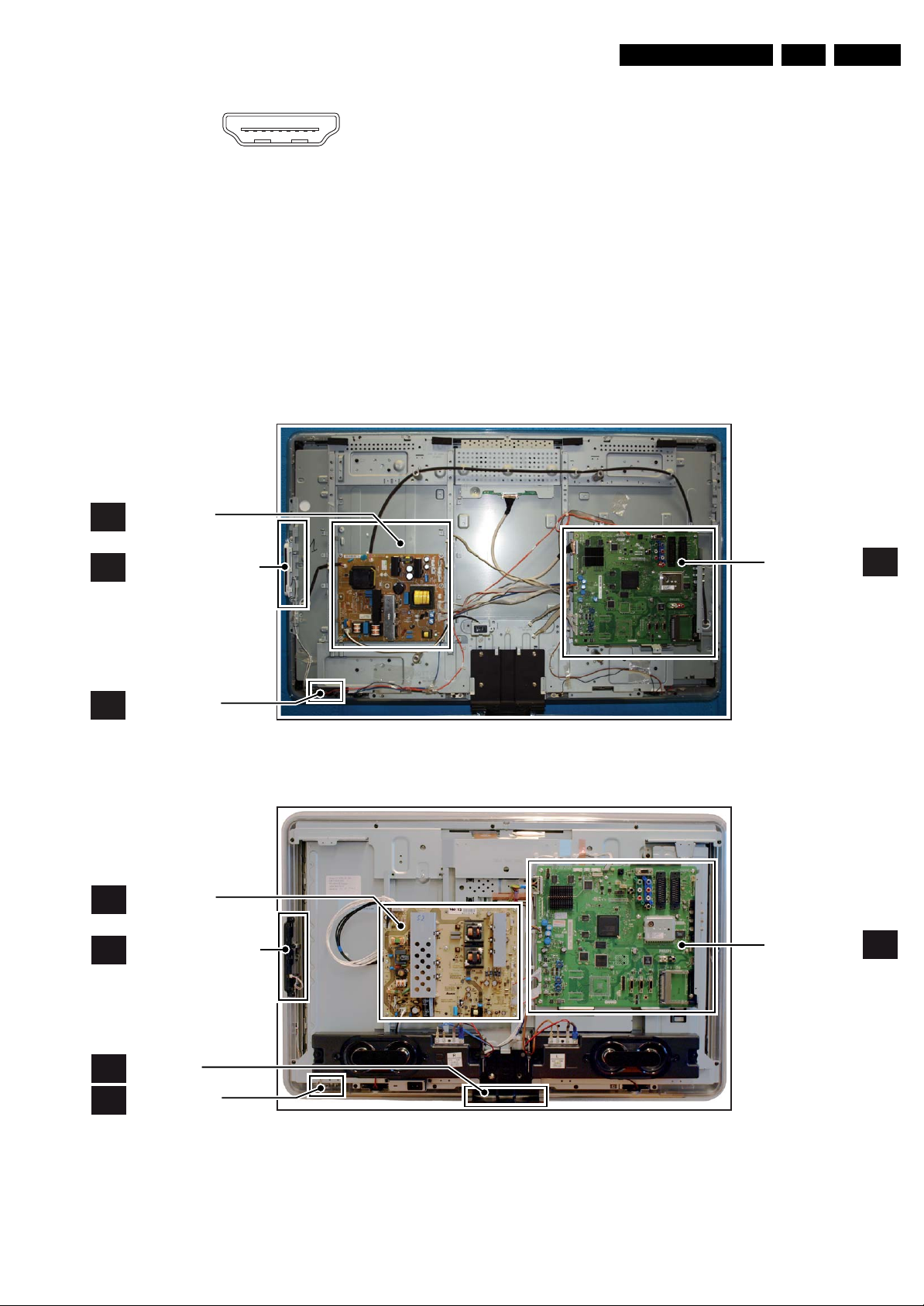
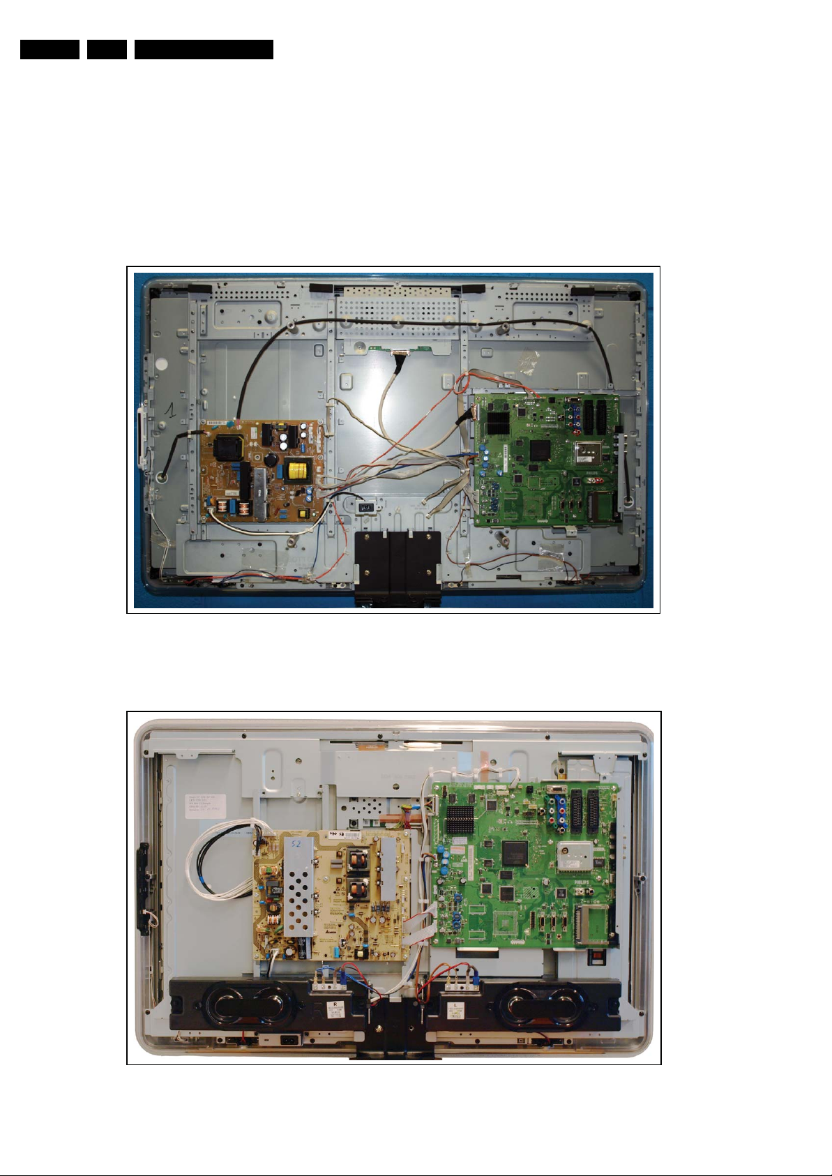
1.3 Chassis Overview
MAIN
A
SUPPLY PANEL
9 -D0- Data channel j
10 - CLK+ Data channel j
11 - Shield Gnd H
12 - CLK- Data channel j
13 - Easylink Control channel jk
14 - n.c.
15 - DDC_SCL DDC clock j
16 - DDC_SDA DDC data jk
17 - Ground Gnd H
18 - +5V j
19 - HPD Hot Plug Detect j
20 - Ground Gnd H
16 - Cinch: Audio - In
Rd - Audio - R 0.5 V
Wh - Audio - L 0.5 V
/ 10 kΩ jq
RMS
/ 10 kΩ jq
RMS
KEYBOARD CONTROL
E
PA NE L
IR & LED PANEL
J
MAIN
A
SUPPLY PANEL
KEYBOARD CONTROL
E
PA NE L
Figure 1-9 PWB/CBA locations 7-series
SMALL SIGNAL
BOARD
I_17661_021.eps
SMALL SIGNAL
BOARD
B
180408
B
LIGHTGUIDE
L
IR & LED PANEL
J
Figure 1-10 PWB/CBA locations 9-series
I_17660_104.eps
130308

EN 6 Q529.1E LA2.
Safety Instructions, Warnings, and Notes
2. Safety Instructions, Warnings, and Notes
Index of this chapter:
2.1 Safety Instructions
2.2 Warnings
2.3 Notes
2.1 Safety Instructions
Safety regulations require the following during a repair:
• Connect the set to the Mains/AC Power via an isolation
transformer (> 800 VA).
• Replace safety components, indicated by the symbol h,
only by components identical to the original ones. Any
other component substitution (other than original type) may
increase risk of fire or electrical shock hazard.
Safety regulations require that after a repair, the set must be
returned in its original condition. Pay in particular attention to
the following points:
• Route the wire trees correctly and fix them with the
mounted cable clamps.
• Check the insulation of the Mains/AC Power lead for
external damage.
• Check the strain relief of the Mains/AC Power cord for
proper function.
• Check the electrical DC resistance between the Mains/AC
Power plug and the secondary side (only for sets that have
a Mains/AC Power isolated power supply):
1. Unplug the Mains/AC Power cord and connect a wire
between the two pins of the Mains/AC Power plug.
2. Set the Mains/AC Power switch to the “on” position
(keep the Mains/AC Power cord unplugged!).
3. Measure the resistance value between the pins of the
Mains/AC Power plug and the metal shielding of the
tuner or the aerial connection on the set. The reading
should be between 4.5 MΩ and 12 MΩ.
4. Switch “off” the set, and remove the wire between the
two pins of the Mains/AC Power plug.
• Check the cabinet for defects, to prevent touching of any
inner parts by the customer.
2.2 Warnings
• All ICs and many other semiconductors are susceptible to
electrostatic discharges (ESD w). Careless handling
during repair can reduce life drastically. Make sure that,
during repair, you are connected with the same potential as
the mass of the set by a wristband with resistance. Keep
components and tools also at this same potential.
• Be careful during measurements in the high voltage
section.
• Never replace modules or other components while the unit
is switched “on”.
• When you align the set, use plastic rather than metal tools.
This will prevent any short circuits and the danger of a
circuit becoming unstable.
2.3 Notes
2.3.1 General
• Measure the voltages and waveforms with regard to the
chassis (= tuner) ground (H), or hot ground (I), depending
on the tested area of circuitry. The voltages and waveforms
shown in the diagrams are indicative. Measure them in the
Service Default Mode (see chapter 5) with a colour bar
signal and stereo sound (L: 3 kHz, R: 1 kHz unless stated
otherwise) and picture carrier at 475.25 MHz for PAL, or
61.25 MHz for NTSC (channel 3).
• Where necessary, measure the waveforms and voltages
with (D) and without (E) aerial signal. Measure the
voltages in the power supply section both in normal
operation (G) and in stand-by (F). These values are
indicated by means of the appropriate symbols.
• Manufactured under license from Dolby Laboratories.
“Dolby”, “Pro Logic” and the “double-D symbol”, are
trademarks of Dolby Laboratories.
2.3.2 Schematic Notes
• All resistor values are in ohms, and the value multiplier is
often used to indicate the decimal point location (e.g. 2K2
indicates 2.2 kΩ).
• Resistor values with no multiplier may be indicated with
either an “E” or an “R” (e.g. 220E or 220R indicates 220 Ω).
• All capacitor values are given in micro-farads (μ=× 10
nano-farads (n =× 10
• Capacitor values may also use the value multiplier as the
decimal point indication (e.g. 2p2 indicates 2.2 pF).
• An “asterisk” (*) indicates component usage varies. Refer
to the diversity tables for the correct values.
• The correct component values are listed in the Spare Parts
List. Therefore, always check this list when there is any
doubt.
2.3.3 BGA (Ball Grid Array) ICs
Introduction
For more information on how to handle BGA devices, visit this
URL: www.atyourservice.ce.philips.com (needs subscription,
not available for all regions). After login, select “Magazine”,
then go to “Repair downloads”. Here you will find Information
on how to deal with BGA-ICs.
BGA Temperature Profiles
For BGA-ICs, you must use the correct temperature-profile,
which is coupled to the 12NC. For an overview of these profiles,
visit the website www.atyourservice.ce.philips.com (needs
subscription, but is not available for all regions)
You will find this and more technical information within the
“Magazine”, chapter “Repair downloads”.
For additional questions please contact your local repair help
desk.
2.3.4 Lead-free Soldering
Due to lead-free technology some rules have to be respected
by the workshop during a repair:
• Use only lead-free soldering tin Philips SAC305 with order
code 0622 149 00106. If lead-free solder paste is required,
please contact the manufacturer of your soldering
equipment. In general, use of solder paste within
workshops should be avoided because paste is not easy to
store and to handle.
• Use only adequate solder tools applicable for lead-free
soldering tin. The solder tool must be able:
– To reach a solder-tip temperature of at least 400°C.
– To stabilize the adjusted temperature at the solder-tip.
– To exchange solder-tips for different applications.
• Adjust your solder tool so that a temperature of around
360°C - 380°C is reached and stabilized at the solder joint.
Heating time of the solder-joint should not exceed ~ 4 sec.
Avoid temperatures above 400°C, otherwise wear-out of
tips will increase drastically and flux-fluid will be destroyed.
To avoid wear-out of tips, switch “off” unused equipment or
reduce heat.
• Mix of lead-free soldering tin/parts with leaded soldering
tin/parts is possible but PHILIPS recommends strongly to
-9
), or pico-farads (p =× 10
-12
-6
),
).

Directions for Use
EN 7Q529.1E LA 3.
avoid mixed regimes. If this cannot be avoided, carefully
clear the solder-joint from old tin and re-solder with new tin.
2.3.5 Alternative BOM identification
It should be noted that: on the European Service website,
“Alternative BOM” is referred to as “Design variant”.
The third digit in the serial number (example:
AG2B0335000001) indicates the number of the alternative
B.O.M. (Bill Of Materials) that has been used for producing the
specific TV set. In general, it is possible that the same TV
model on the market is produced with e.g. two different types
of displays, coming from two different suppliers. This will then
result in sets which have the same CTN (Commercial Type
Number; e.g. 28PW9515/12) but which have a different B.O.M.
number.
By looking at the third digit of the serial number, one can
identify which B.O.M. is used for the TV set he is working with.
If the third digit of the serial number contains the number “1”
(example: AG1B033500001), then the TV set has been
manufactured according to B.O.M. number 1. If the third digit is
a “2” (example: AG2B0335000001), then the set has been
produced according to B.O.M. no. 2. This is important for
ordering the correct spare parts!
For the third digit, the numbers 1...9 and the characters A...Z
can be used, so in total: 9 plus 26= 35 different B.O.M.s can be
indicated by the third digit of the serial number.
Identification: The bottom line of a type plate gives a 14-digit
serial number. Digits 1 and 2 refer to the production center (e.g.
AG is Bruges), digit 3 refers to the B.O.M. code, digit 4 refers
to the Service version change code, digits 5 and 6 refer to the
production year, and digits 7 and 8 refer to production week (in
example below it is 2006 week 17). The 6 last digits contain the
serial number.
MODEL :
PROD.NO:
2.3.6 Board Level Repair (BLR) or Component Level Repair
(CLR)
If a board is defective, consult your repair procedure to decide
if the board has to be exchanged or if it should be repaired on
component level.
If your repair procedure says the board should be exchanged
completely, do not solder on the defective board. Otherwise, it
cannot be returned to the O.E.M. supplier for back charging!
2.3.7 Practical Service Precautions
• It makes sense to avoid exposure to electrical shock.
• Always respect voltages. While some may not be
32PF9968/10
AG 1A0617 000001
Figure 2-1 Serial number (example)
While some sources are expected to have a possible
dangerous impact, others of quite high potential are of
limited current and are sometimes held in less regard.
dangerous in themselves, they can cause unexpected
reactions that are best avoided. Before reaching into a
powered TV set, it is best to test the high voltage insulation.
It is easy to do, and is a good service precaution.
MADE IN BELGIUM
220-240V 50/60Hz
~
VHF+S+H+UHF
BJ3.0E LA
S
E_06532_024.eps
128W
260308
3. Directions for Use
You can download this information from the following websites:
http://www.philips.com/support
http://www.p4c.philips.com
EN 8 Q529.1E LA4.
Mechanical Instructions
4. Mechanical Instructions
Index of this chapter:
4.1 Cable Dressing
4.2 Service Positions
4.3 Assy/Panel Removal VE8 Styling
4.4 Assy/Panel Removal ME8+ Styling
4.5 Set Re-assembly.
4.1 Cable Dressing
Notes:
• Figures below can deviate slightly from the actual situation,
due to the different set executions.
Figure 4-1 Cable dressing 7-series
I_17661_022.eps
180408
Figure 4-2 Cable dressing 9-series
I_17660_105.eps
130308
4.2 Service Positions
For easy servicing of this set, there are a few possibilities
created:
• The buffers from the packaging (see figure “Rear cover”).
• Foam bars (created for Service).
4.2.1 Foam Bars
1
Required for sets
1
42"
E_06532_018.eps
171106
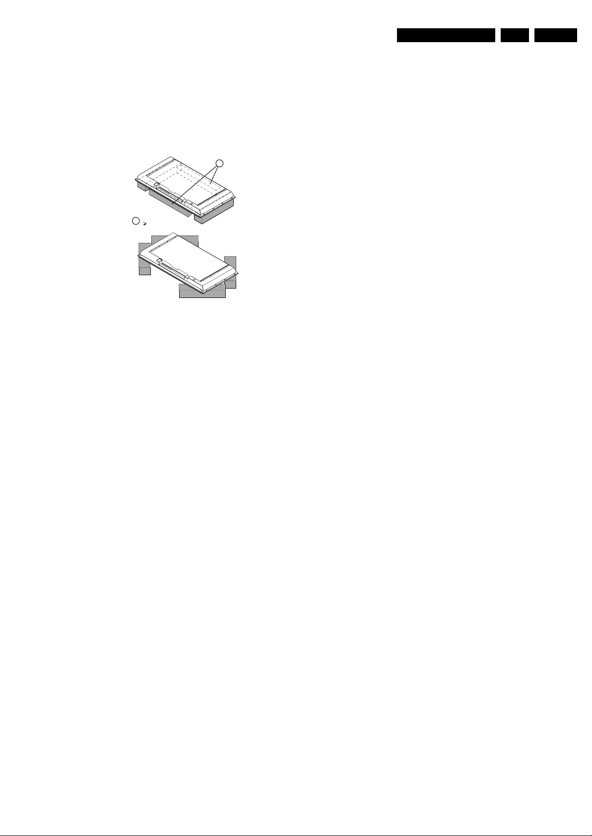
Figure 4-3 Foam bars
Mechanical Instructions
EN 9Q529.1E LA 4.
The foam bars (order code 3122 785 90580 for two pieces) can
be used for all types and sizes of Flat TVs. See figure “Foam
bars” for details. Sets with a display of 42" and larger, require
four foam bars [1]. Ensure that the foam bars are always
supporting the cabinet and never only the display.
Caution: Failure to follow these guidelines can seriously
damage the display!
By laying the TV face down on the (ESD protective) foam bars,
a stable situation is created to perform measurements and
alignments. By placing a mirror under the TV, the screen can
be monitored.
EN 10 Q529.1E LA4.
Mechanical Instructions
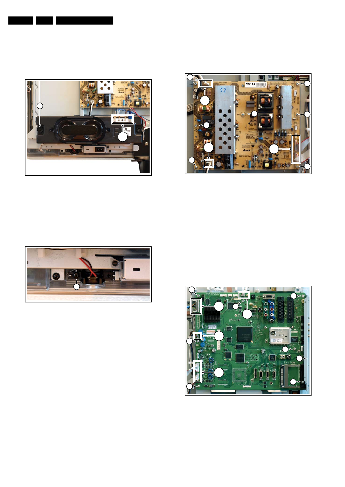
4.3 Assy/Panel Removal VE8 Styling
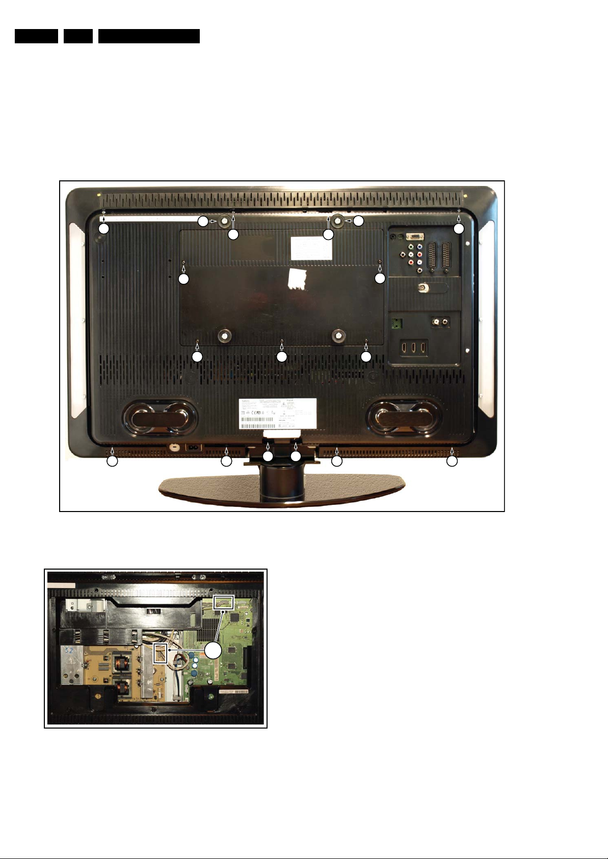
4.3.1 Rear Cover
Warning: Disconnect the mains power cord before removing
the rear cover.
Note: It is necessity to release the fixation screws from the
stand before removing the rear cover.
Refer to next figures for details.
5
2
1
5 5
1. Remove the mushrooms [1].
2. Remove the fixation screws [2] from the hatch and lift the
hatch from the rear cover.
3. Unplug the connectors [3].
4. Remove the fixation screws from the stand. Please note
that the set is now mechanically not secured and may be
unstable.
5. Remove the fixation screws [5] that secure the rear cover.
6. Lift the rear cover from the TV. Make sure that wires and
flat foils are not damaged while lifting the rear cover from
the set.
1
5
2
222
5
4 4
555
I_17660_106.eps
130308
Figure 4-4 Rear Cover
3
Figure 4-5 Hatch
I_17660_107.eps
130308
Mechanical Instructions
EN 11Q529.1E LA 4.
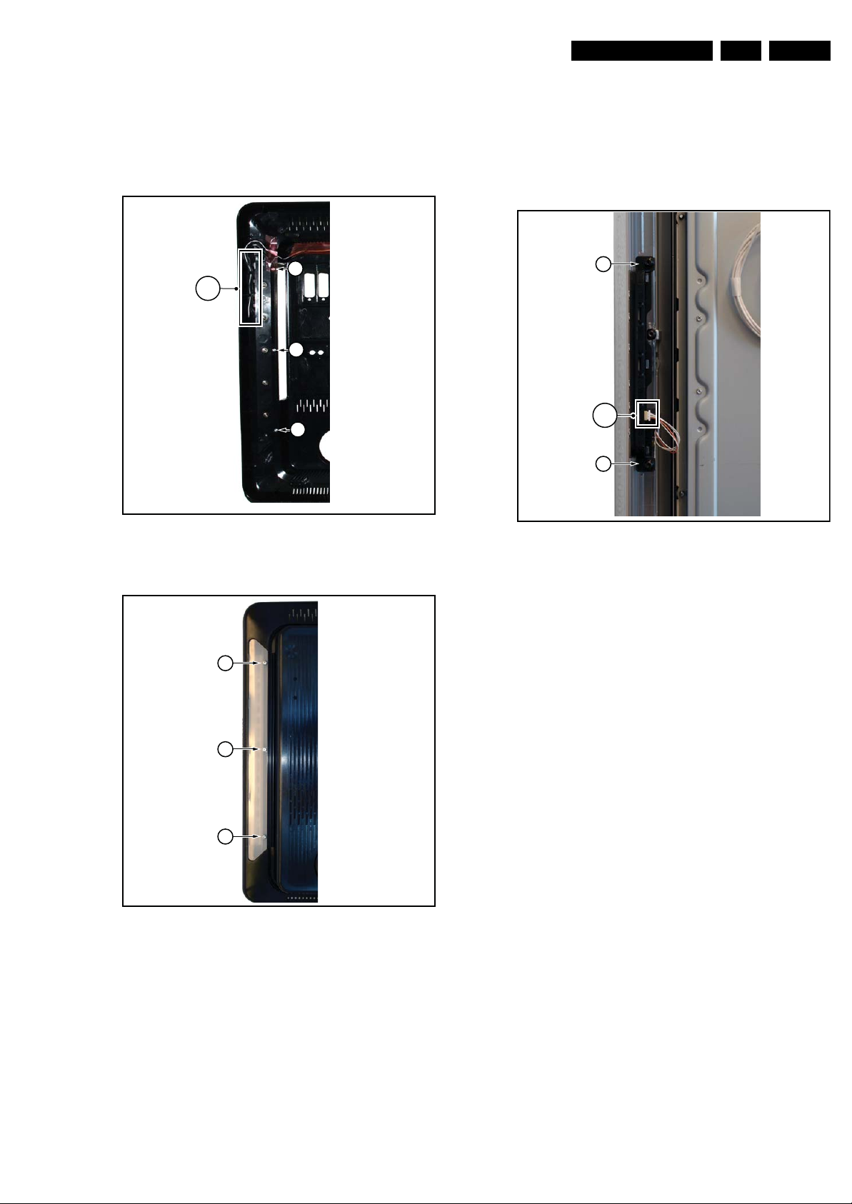
4.3.2 Ambilight
Refer to next figure for details.
1. Release the wire from the wire guides [1].
2. Remove the fixation screws [2].
3. Remove the cover screws [3] and take out the whole unit.
When defective, replace the whole unit.
2
1
2
2
4.3.3 Key Board
Refer to next figure for details.
1. Unplug the key board connector [1] from the IR & LED
board.
2. Remove the screws [2].
3. Lift the unit and take it out of the set.
When defective, replace the whole unit.
2
1
2
Figure 4-6 Ambilight inside cover
3
3
3
I_17660_108.eps
130308
I_17660_109.eps
130308
Figure 4-8 Key Board
I_17660_110.eps
130308
Figure 4-7 Ambilight outside cover
EN 12 Q529.1E LA4.
Mechanical Instructions
4.3.4 Bass-midrange Speakers
Refer to next figure for details.
1. Release the speaker connectors [1] from unit.
2. Remove the screw [1] and lift the whole unit from the set.
Take the speakers out together with their casing. When
defective, replace the whole unit.
2
Figure 4-9 Bass-midrange Speaker
1
I_17660_111.eps
130308
4.3.6 Display Supply Panel
Refer to next figure for details.
1. Unplug the connectors [1].
2. Remove the fixation screws [2].
3. Take the board out.
2
1
2
1
2
Figure 4-11 Display Supply Panel
2
2
2
(
2x
)
2
2
I_17660_113.eps
130308
4.3.5 Tweeters
Refer to next figure for details.
1. Remove the bass-midrange speaker as described earlier.
2. Remove the screw [1] and lift the whole unit from the set.
When defective, replace the whole unit.
1
Figure 4-10 Tweeters
I_17660_112.eps
130308
4.3.7 Small Signal Board (SSB)
Refer to next figure for details.
Caution: it is mandatory to remount all different screws at their
original position during re-assembly. Failure to do so may result
in damaging the SSB.
Refer to next figures or details.
1. Unplug the LVDS connector [1].
Caution: be careful, as this is a very fragile connector!
2. Unplug the connectors [2].
3. Remove the screw [3] from the side I/O cover.
4. Remove the fixation screws [4].
5. The SSB can now be taken out of the set.
4
1
4
2
2
4
2
(2x)
4
4
4
3
4
Figure 4-12 Small Signal Board
I_17660_114.eps
130308
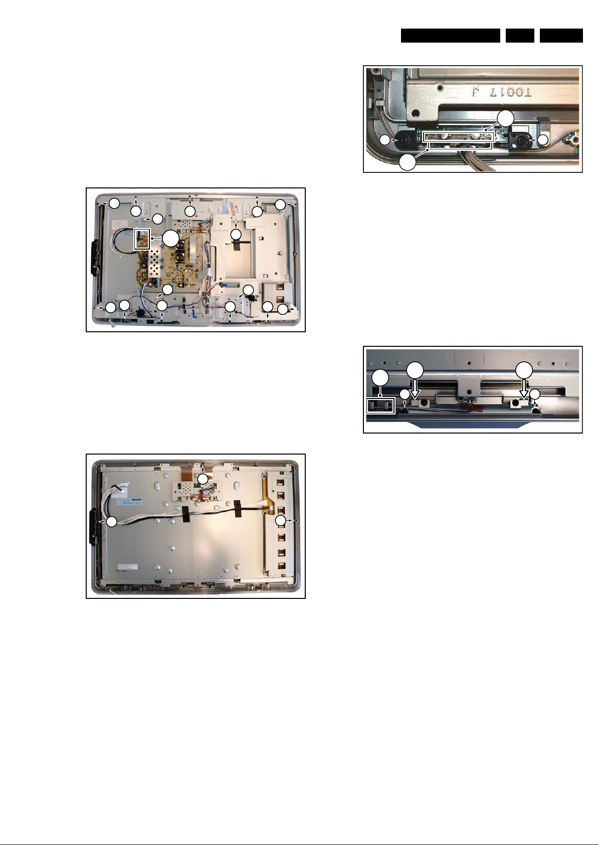
4.3.8 LCD Panel
Refer to next figure for details.
1. Remove the SSB as described earlier.
2. Remove the Bass-midrange speakers as described earlier.
3. Remove the Tweeters as described earlier.
4. Unplug the connectors [1].
5. Remove the fixation screws [2].
6. Remove the fixation screws [3].
7. Lift out the sub frame.
8. The LCD panel can now be lifted from the front cabinet.
When defective, replace the whole unit.
Mechanical Instructions
1
EN 13Q529.1E LA 4.
2
3x)
(
1
2
I_17660_117.eps
290408
2
2
3
2
1
(
2x
)
3
3
2
2
2
Figure 4-13 LCD Panel
4.3.9 Rim
Refer to next figure for details.
1. Do all steps as described in the removal of the LCD panel
except the last step.
2. Remove the screws [1].
1
2
3
22
I_17660_115.eps
2
2
130308
Figure 4-15 IR & LED Board
4.3.11 Lightguide
Refer to next figure for details.
1. Do all steps as described in the removal of the Rim.
2. Release the cables from the cable clamps [1].
3. Remove screws [2] and lift the lightguide from the front
cover.
4. Release the board by pushing up the clamps in the
direction of the arrows.
5. Remove the unit from the front cover.
When defective, replace the whole unit.
1
3 3
2 2
Figure 4-16 IR & LED Board
4.4 Assy/Panel Removal ME8+ Styling
I_17660_118.eps
140308
1
Figure 4-14 Rim
4.3.10 IR & LED Board
Refer to next figure for details.
1. Do all steps as described in the removal of the Rim.
2. Remove screws [1] and lift the IR & LED Board from the
front cover.
3. Lift the board and take it out of the set.
4. Release the cables from the cable clamps.
5. Unplug the connectors [3].
When defective, replace the whole unit.
1
I_17660_116.eps
130308
Refer to the Q528.2E LA Service Manual.
4.5 Set Re-assembly
To re-assemble the whole set, execute all processes in reverse
order.
Notes:
• While re-assembling, make sure that all cables are placed
and connected in their original position. See figure “Cable
dressing”.
• Pay special attention not to damage the EMC foams on the
SSB shields. Ensure that EMC foams are mounted
correctly.
EN 14 Q529.1E LA5.
Service Modes, Error Codes, and Fault Finding
5. Service Modes, Error Codes, and Fault Finding
Index of this chapter:
5.1 Test Points
5.2 Service Modes
5.3 Stepwise Start-up
5.4 Service Tools
5.5 Error Codes
5.6 The Blinking LED Procedure
5.7 Protections
5.8 Fault Finding and Repair Tips
5.9 Software Upgrading
5.1 Test Points
As most signals are digital, it will be difficult to measure
waveforms with a standard oscilloscope. However, several key
ICs are capable of generating test patterns, which can be
controlled via ComPair. In this way it is possible to determine
which part is defective.
Perform measurements under the following conditions:
• Service Default Mode.
• Video: Colour bar signal.
• Audio: 3 kHz left, 1 kHz right.
5.2 Service Modes
Service Default mode (SDM) and Service Alignment Mode
(SAM) offers several features for the service technician, while
the Customer Service Mode (CSM) is used for communication
between the call centre and the customer.
This chassis also offers the option of using ComPair, a
hardware interface between a computer and the TV chassis. It
offers the abilities of structured troubleshooting, error code
reading, and software version read-out for all chassis.
(see also section “5.4.1 ComPair”).
5.2.1 Service Default Mode (SDM)
– Skip/blank of non-favourite pre-sets.
How to Activate SDM
For this chassis there are two kinds of SDM: an analog SDM
and a digital SDM. Tuning will happen according table “SDM
Default Settings”.
• Analog SDM: use the standard RC-transmitter and key in
the code “062596”, directly followed by the “MENU” button.
Note: It is possible that, together with the SDM, the main
menu will appear. To switch it “off”, push the “MENU”
button again.
• Digital SDM: use the standard RC-transmitter and key in
the code “062593”, directly followed by the “MENU” button.
Note: It is possible that, together with the SDM, the main
menu will appear. To switch it “off”, push the “MENU”
button again.
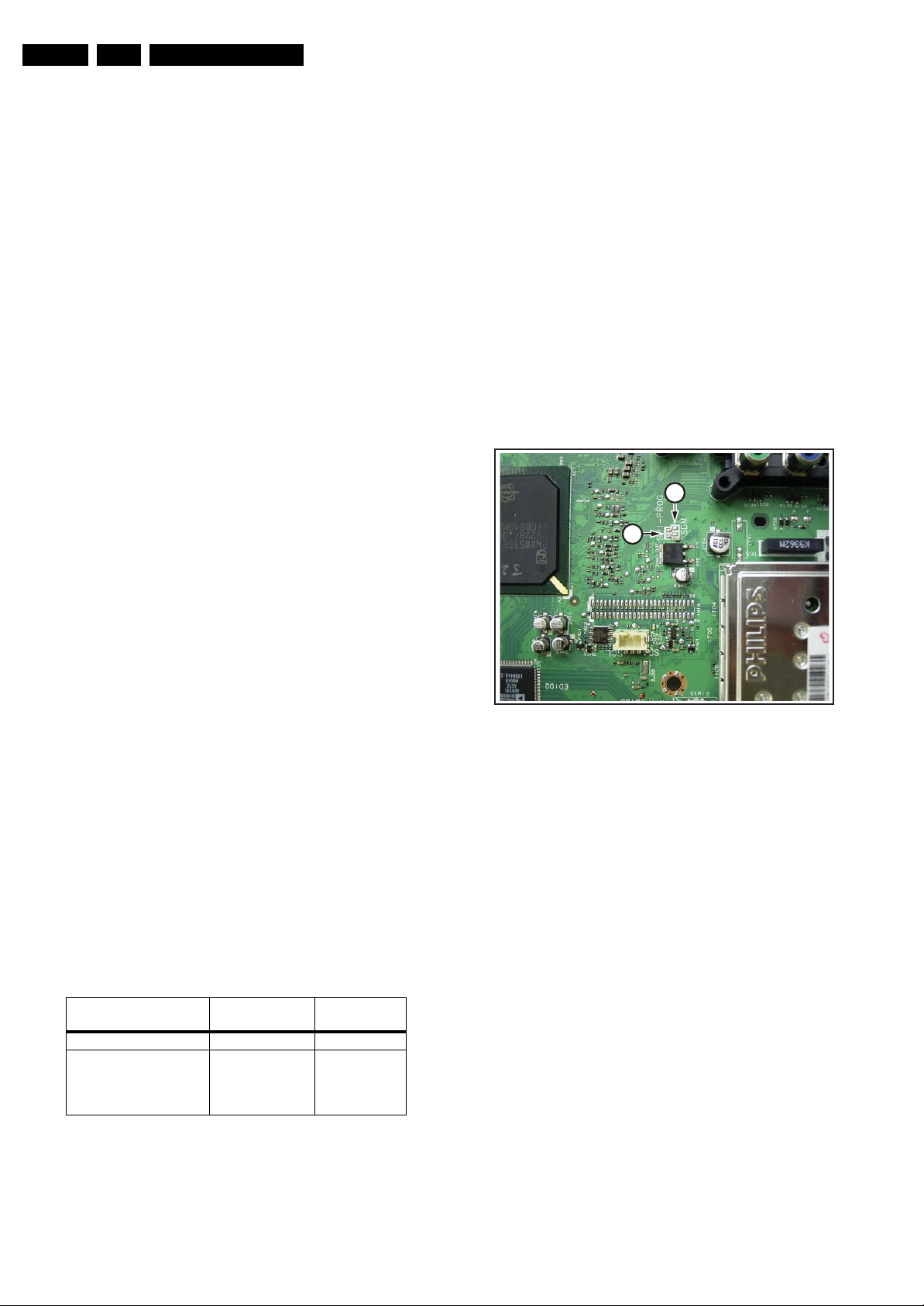
• Analog SDM can also be activated by shorting for a
moment the two solder pads (see figure “Service mode
pads”) on the SSB, with the indication “SDM”.
1
2
H_16770_100.eps
130707
Figure 5-1 Service mode pads
Purpose
• To create a pre-defined setting, to get the same
measurement results as given in this manual.
• To override SW protections detected by stand-by
processor and make the TV start up to the step just before
protection (a sort of automatic stepwise start up). See
section “5.3 Stepwise Start-up”.
• To start the blinking LED procedure where only layer 2
errors are displayed. (see also section “5.5 Error Codes”)
Specifications
Table 5-1 SDM default settings
Default
Region Freq. (MHz)
Europe, AP(PAL/Multi) 475.25 PAL B/G
Europe, AP DVB-T 546.00 PID
Video: 0B 06 PID
PCR: 0B 06 PID
Audio: 0B 07
• All picture settings at 50% (brightness, colour, contrast).
• All sound settings at 50%, except volume at 25%.
• All service-unfriendly modes (if present) are disabled, like:
– (Sleep) timer.
– Child/parental lock.
– Picture mute (blue mute or black mute).
– Automatic volume levelling (AVL).
system
DVB-T
After activating this mode, “SDM” will appear in the upper right
corner of the screen (when a picture is available).
How to Navigate
When the “MENU” button is pressed on the RC transmitter, the
set will toggle between the SDM and the normal user menu
(with the SDM mode still active in the background).
How to Exit SDM
Use one of the following methods:
• Switch the set to STAND-BY via the RC-transmitter.
• Via a standard customer RC-transmitter: key in “00”sequence.
5.2.2 Service Alignment Mode (SAM)
Purpose
• To perform (software) alignments.
• To change option settings.
• To easily identify the used software version.
• To view operation hours.
• To display (or clear) the error code buffer.
How to Activate SAM
Via a standard RC transmitter: key in the code “062596”
directly followed by the “INFO” button. After activating SAM
with this method a service warning will appear on the screen,
continue by pressing the red button on the RC.

Service Modes, Error Codes, and Fault Finding
Contents of SAM:
• Hardware Info.
– A. SW Version. Displays the software version of the
main software (example: Q591E-1.2.3.4 =
AAAAB_X.Y.W.Z).
• AAAA= the chassis name.
• B= the region: A= AP, E= EU, L= LatAm, U = US.
For AP sets it is possible that the Europe software
version is used.
• X.Y.W.Z= the software version, where X is the
main version number (different numbers are not
compatible with one another) and Y.W.Z is the sub
version number (a higher number is always
compatible with a lower number).
– B. SBY PROC Version. Displays the software version
of the stand-by processor.
– C. Production Code. Displays the production code of
the TV, this is the serial number as printed on the back
of the TV set. Note that if an NVM is replaced or is
initialized after corruption, this production code has to
be re-written to NVM. ComPair will foresee in a
possibility to do this.
• Operation Hours. Displays the accumulated total of
operation hours (not the stand-by hours). Every time the
TV is switched “on/off”, 0.5 hours is added to this number.
• Errors (followed by maximum 10 errors). The most recent
error is displayed at the upper left (for an error explanation
see section “5.5 Error Codes”).
• Reset Error Buffer. When “cursor right” (or the “OK
button) is pressed and then the “OK” button is pressed, the
error buffer is reset.
• Alignments. This will activate the “ALIGNMENTS” submenu.
• Dealer Options. Extra features for the dealers.
• Options. Extra features for Service. For more info
regarding option codes, see chapter 8 “Alignments”.
Note that if the option code numbers are changed, these
have to be confirmed with pressing the “OK” button before
the options are stored. Otherwise changes will be lost.
• Initialize NVM. The moment the processor recognizes a
corrupted NVM, the “initialize NVM” line will be highlighted.
Now, two things can be done (dependent of the service
instructions at that moment):
– Save the content of the NVM via ComPair for
development analysis, before initializing. This will give
the Service department an extra possibility for
diagnosis (e.g. when Development asks for this).
– Initialize the NVM.
Note: When the NVM is corrupted, or replaced, there is a high
possibility that no picture appears because the display code is
not correct. So, before initializing the NVM via the SAM, a
picture is necessary and therefore the correct display option
has to be entered. Refer to chapter 8 “Alignments” for details.
To adapt this option, it’s advised to use ComPair (the correct
HEX values for the options can be found in chapter 8
“Alignments”) or a method via a standard RC (described
below).
Changing the display option via a standard RC: Key in the
code “062598” directly followed by the “MENU” button and
“XXX” (where XXX is the 3 digit decimal display code as
mentioned in table “Option code overview” in chapter 8
“Alignments”). Make sure to key in all three digits, also the
leading zero’s. If the above action is successful, the front LED
will go out as an indication that the RC sequence was correct.
After the display option is changed in the NVM, the TV will go
to the Stand-by mode. If the NVM was corrupted or empty
before this action, it will be initialized first (loaded with default
values). This initializing can take up to 20 seconds.
EN 15Q529.1E LA 5.
Display Option
Code
39mm
040
PHILIPS
MODEL:
32PF9968/10
27mm
PROD.SERIAL NO:
AG 1A0620 000001
(CTN Sticker)
E_06532_038.eps
240108
Figure 5-2 Location of Display Option Code sticker
• Store - go right. All options and alignments are stored
when pressing “cursor right” (or the “OK” button) and then
the “OK”-button.
• SW Maintenance.
– SW Events. Not useful for Service purposes. In case
of specific software problems, the development
department can ask for this info.
– HW Events. Not useful for Service purposes. In case
of specific software problems, the development
department can ask for this info.
• Test settings. For development purposes only.
• Upload to USB. To upload several settings from the TV to
an USB stick, which is connected to the SSB. The items are
“Channel list”, “Personal settings”, “Option codes”,
“Display-related alignments” and “History list”. First a
directory “repair\” has to be created in the root of the USB
stick. To upload the settings select each item separately,
press “cursor right” (or the “OK button), confirm with “OK”
and wait until “Done” appears. In case the download to the
USB stick was not successful “Failure” will appear. In this
case, check if the USB stick is connected properly and if
the directory “repair” is present in the root of the USB stick.
Now the settings are stored onto the USB stick and can be
used to download onto another TV or other SSB.
Uploading is of course only possible if the software is
running and if a picture is available. This method is created
to be able to save the customer’s TV settings and to store
them into another SSB.
• Download to USB. To download several settings from the
USB stick to the TV. Same way of working as with
uploading. To make sure that the download of the channel
list from USB to the TV is executed properly, it is necessary
to restart the TV and tune to a valid preset if necessary.
Note: The “History list item” can not be downloaded from
USB to the TV. This is a “read-only” item. In case of
specific problems, the development department can ask
for this info.
• Development file versions. Not useful for Service
purposes, this information is only used by the development
department.
How to Navigate
• In SAM, the menu items can be selected with the
“CURSOR UP/DOWN” key (or the scroll wheel) on the RCtransmitter. The selected item will be highlighted. When not
all menu items fit on the screen, move the “CURSOR UP/
DOWN” key to display the next/previous menu items.
• With the “CURSOR LEFT/RIGHT” keys (or the scroll
wheel), it is possible to:
– (De) activate the selected menu item.
– (De) activate the selected sub menu.
• With the “OK” key, it is possible to activate the selected
action.
How to Exit SAM
Use one of the following methods:
• Press the “MENU” button on the RC-transmitter.

EN 16 Q529.1E LA5.
Service Modes, Error Codes, and Fault Finding
• Switch the set to STAND-BY via the RC-transmitter.
5.2.3 Customer Service Mode (CSM)
Purpose
When a customer is having problems with his TV-set, he can
call his dealer or the Customer Helpdesk. The service
technician can then ask the customer to activate the CSM, in
order to identify the status of the set. Now, the service
technician can judge the severity of the complaint. In many
cases, he can advise the customer how to solve the problem,
or he can decide if it is necessary to visit the customer.
The CSM is a read only mode; therefore, modifications in this
mode are not possible.
When in this chassis CSM is activated, a testpattern will be
displayed during 5 seconds (1 second Blue, 1 second Green
and 1 second Red, then again 1 second Blue and 1 second
Green). This test pattern is generated by the PNX5100. So if
this test pattern is shown, it could be determined that the back
end video chain (PNX5100, LVDS, and display) of the SSB is
working.
To determine if the MPEG4-circuit is working (in case of an
MPEG4-set), push the “MUTE” button during CSM to display
another test pattern. This is a forced input selection to make
sure the test pattern is visible. If this test pattern is not shown,
it is possible that the settings are not correct (for instance in
SAM the MPEG4-option is “NOT PRESENT”). The display of
this test pattern is a toggle function, pressing the “MUTE” key
again removes this test pattern.
When CSM is activated and there is a USB stick connected to
the TV, the software will dump the complete CSM content to the
USB stick. The file (Csm.txt) will be saved in the root of the USB
stick. This info can be handy if no information is displayed.
Also when CSM is activated, the layer 1 error is displayed via
blinking LED. Only the latest error is displayed. (see also
section “5.5 Error Codes”).
How to Activate CSM
Key in the code “123654” via the standard RC transmitter.
Note: Activation of the CSM is only possible if there is no (user)
menu on the screen!
How to Navigate
By means of the “CURSOR-DOWN/UP” knob (or the scroll
wheel) on the RC-transmitter, can be navigated through the
menus.
Contents of CSM
The contents are reduced to 3 pages: General, Software
versions and Quality items. The group names itself are not
shown anywhere in the CSM menu.
General
• Set Type. This information is very helpful for a helpdesk/
workshop as reference for further diagnosis. In this way, it
is not necessary for the customer to look at the rear of the
TV-set. Note that if an NVM is replaced or is initialized after
corruption, this set type has to be re-written to NVM.
ComPair will foresee in a possibility to do this.
• Production Code. Displays the production code (the serial
number) of the TV. Note that if an NVM is replaced or is
initialized after corruption, this production code has to be
re-written to NVM. ComPair will foresee a in possibility to
do this.
• Installed date. Indicates the date of the first installation of
the TV. This date is acquired via time extraction.
• Options 1. Gives the option codes of option group 1 as set
in SAM (Service Alignment Mode).
• Options 2. Gives the option codes of option group 2 as set
in SAM (Service Alignment Mode).
• 12NC SSB. Gives an identification of the SSB as stored in
NVM. Note that if an NVM is replaced or is initialized after
corruption, this identification number has to be re-written to
NVM. ComPair will foresee in a possibility to do this. This
identification number is the 12nc number of the SSB.
Remark: the content here can also be a part of the 12NC
of the SSB in combination with the serial number.
• 12NC display. Shows the 12NC of the display
• 12NC supply. Shows the 12NC of the supply.
• 12NC “bolt-on”. Shows the 12NC of the “BOLT-ON”module.
Software versions
• Current main SW. Displays the built-in main software
version. In case of field problems related to software,
software can be upgraded. As this software is consumer
upgradeable, it will also be published on the Internet.
Example: Q591E_1.2.3.4
• Standby SW. Displays the built-in stand-by processor
software version. Upgrading this software will be possible
via ComPair or via USB (see chapter Software upgrade).
Example: STDBY_3.0.1.2.
• MOP ambient light SW. Displays the MOP ambient light
EPLD SW.
• MPEG4 software. Displays the MPEG4 software (optional
for sets with MPEG4).
• PNX5100 boot NVM. Displays the SW-version that is used
in the PNX5100 boot NVM.
Quality items
• Signal quality. Poor / average /good
• Child lock. Not active / active. This is a combined item for
locks. If any lock (Preset lock, child lock, lock after or
parental lock) is active, the item shall show “active”.
• Table channel changed. This item is for development
purpose, it will be defined later.
• Key missing. This is a combined item for keys. The keys
have a separate bit and the sum is displayed in decimal
value.
– HDMI key valid = 001
– MAC key valid = 010
Important remark here : due to a software bug, the
MAC key is missing and not valid when “2” is displayed
in CSM.So, if for instance the HDMI and MAC keys are
both valid, the decimal value in CSM “1” is displayed
and not “3”.
– BDS key valid = 100
If 3 keys are valid the value: “5” is displayed(should be
“7” but due to the software bug).
– For value:
“0” in CSM: MAC address stored, HDCP invalid.
“1” in CSM: MAC address stored, HDCP valid.
“2” in CSM: no MAC address stored, HDCP invalid.
“3” in CSM: no MAC address stored, HDCP valid.
• CI slot present. If the common interface module is
detected the result will be “YES”, else “NO”.
• HDMI input format. The detected input format of the
HDMI.
• HDMI audio input stream. The HDMI audio input stream
is displayed: present / not present.
• HDMI video input stream. The HDMI video input stream
is displayed: present / not present.
How to Exit CSM
Press “MENU” on the RC-transmitter.
Service Modes, Error Codes, and Fault Finding
EN 17Q529.1E LA 5.
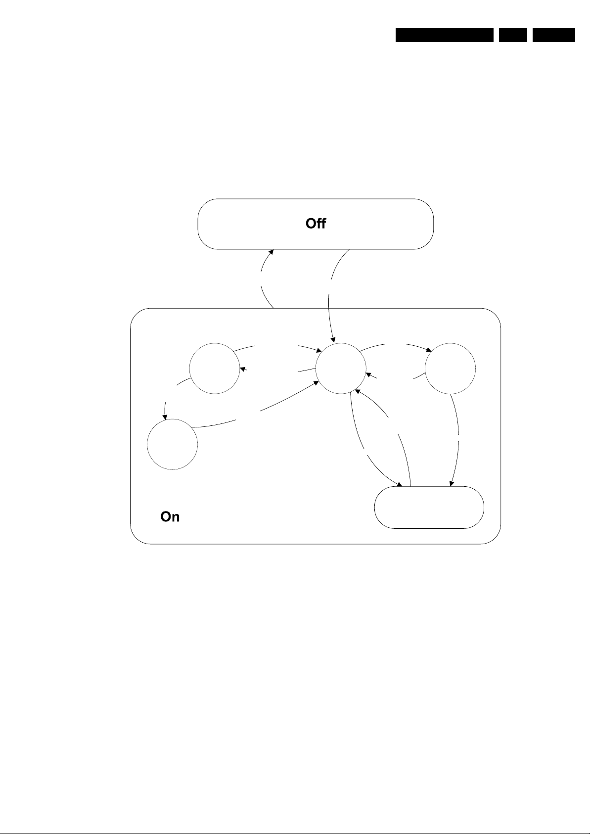
5.3 Stepwise Start-up
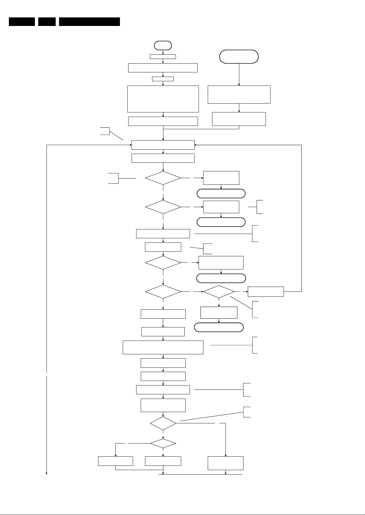
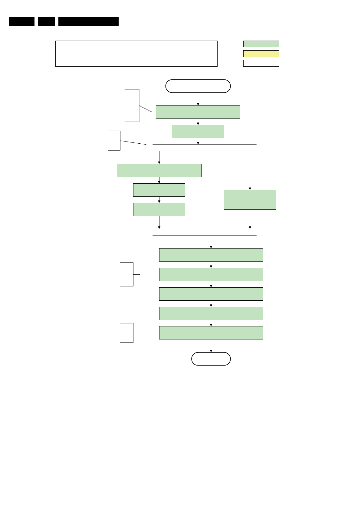
When the TV is in a protection state due to an error detected by
stand-by software (error blinking is displayed) and SDM is
activated via shortcutting the pins on the SSB, the TV starts up
until it reaches the situation just before protection. So, this is a
kind of automatic stepwise start-up. In combination with the
start-up diagrams below, you can see which supplies are
present at a certain moment. Important to know is, that if e.g.
the 3V3 detection fails and thus error layer 2 = 18 is blinking
while the TV is restarted via SDM, the Stand-by Processor will
enable the 3V3, but the TV set will not go to protection now.
The TV will stay in this situation until it is reset (Mains/AC
Power supply interrupted). Caution: in case the start up in this
St by
-Tact switch Pushed
-last status is hibernate
after mains ON
Tact switch
Hibernate
Mains
off
-WakeUp requested
-Acquisition needed
-No data Acquisition
required
-tact SW pushed
-last status is hibernate
after mains ON
pushed
Mains
on
Semi
St by
mode with a faulty FET 7U08 is done, you can destroy all IC’s
supplied by the +3V3, due to overvoltage (12V on 3V3-line). It
is recommended to measure first the FET 7U08 or others
FET’s on shortcircuit before activating SDM via the service
pads.
The abbreviations “SP” and “MP” in the figures stand for:
• SP: protection or error detected by the Stand-by
Processor.
• MP: protection or error detected by the MIPS Main
Processor.
WakeUp
requested
Active
- St by requested
-tact SW pushed
WakeUp
requested
(SDM)
GoToProtection
GoToProtection
Figure 5-3 Transition diagram
Protection
I_17660_124.eps
140308
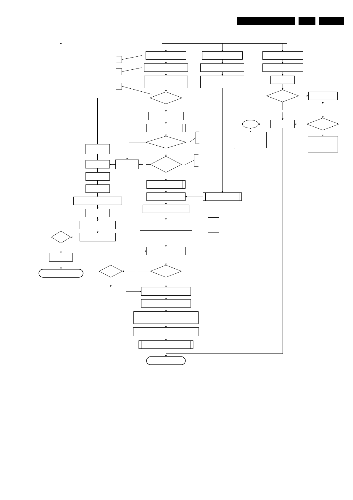
EN 18 Q529.1E LA5.
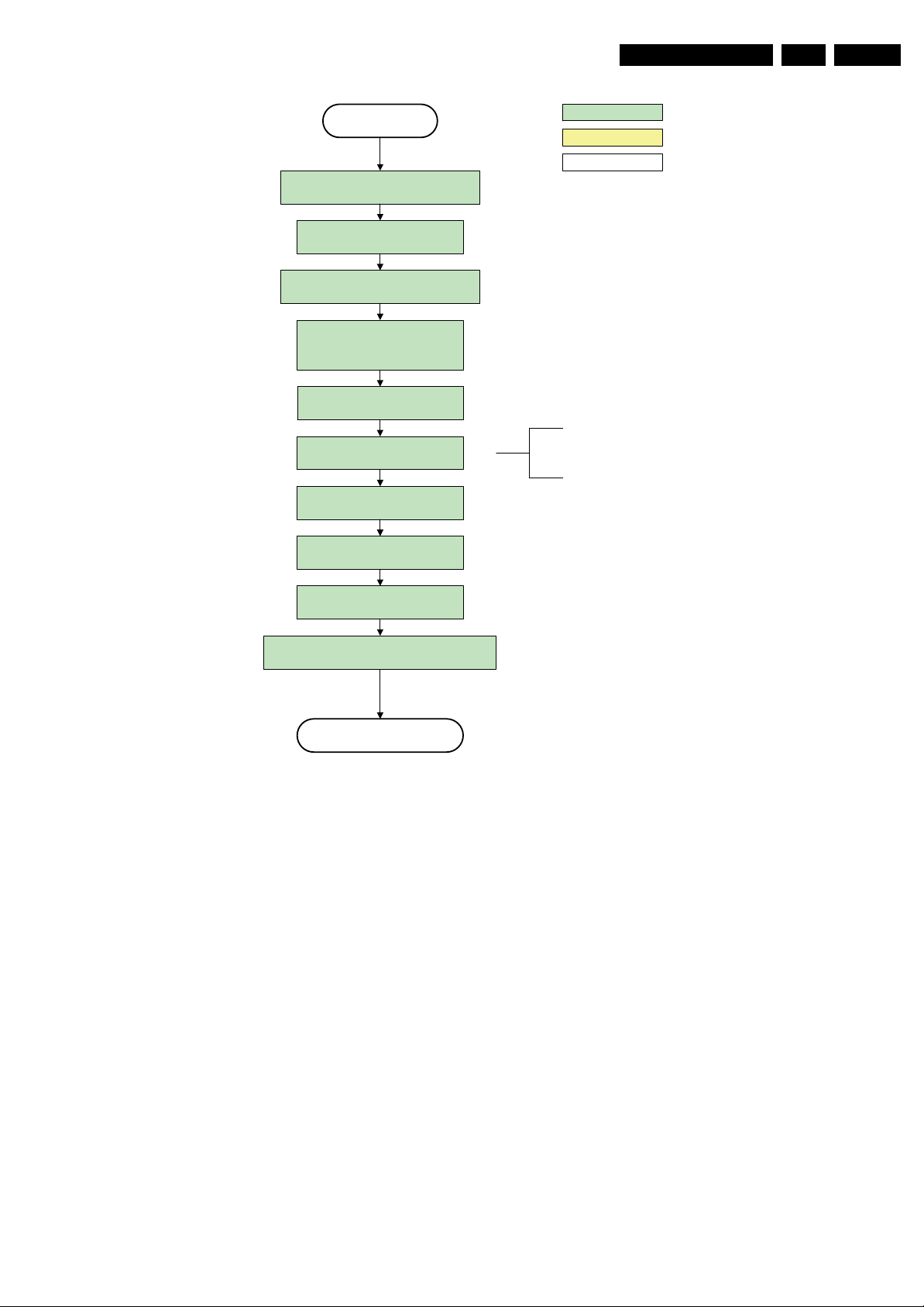
Important remark; the appearance of the +12V
will start the +1V2 DCDC converter automatically
Service Modes, Error Codes, and Fault Finding
Off
Mains is app lied
Standby Supply starts running.
All standby supply voltages become available .
st-by µ P resets
Initialise I/O pins of the st-by µP:
- Switch reset-AVCLOW (reset state)
- Switch WP-NandFlash LOW (protected)
- Switch reset-system LOW (reset state)
- Switch reset-5100 LOW (reset state)
- Switch reset-Ethernet LOW (reset state)
- Switch reset-ST7100 LOW (reset state)
- keep reset-NVM high, Audio-reset and Audio-Mute-Up HIGH
start keyboard scanning, RC detection. Wake up reasons are
Switch ON Platform and display supply by switching
+12V, +/-12Vs, AL and Bolt-on power
is switched on, followed by the +1V2 DCDC converter
off.
LOW the Standby line.
Stand by or
Protection
If the protection state was left by short circuiting the
SDM pins, detection of a protection condition during
startup will stall the startup. Protection conditions in a
playing set will be ignored. The protection mode will
not be entered.
- Switch Audio-Reset high.
It is low in the standby mode if the standby
mode lasted longer than 10s.
Detect2 should be polled on the standard 40ms
interval and startup should be continued when
detect2 becomes high.
Switch LOW the RESET-NVM line to allow access to NVM. (Add a
2ms delay before trying to address the NVM to allow correct NVM
initialization, this is not issue in this setup, the delay is automatically
No
No
Release AVC system r eset
Feed warm boot script
To I_17660_125b.eps To I_17660_125b.eps
Detect2 high received
within 1 second?
Yes
Supply-fault I/O
High?
Yes
Enable the DCDC converter for +3V3 and
+5V. (EN ABLE-3V3)
Wait 50ms
Supply-fault I/O
High?
yes
Detect-1 I/O line
High?
Yes
Enable the supply fault detection
algorithm
Set I²C slave address
of Standby µP to (A0h)
covered by the architectural setup)
Switch HIGH the WP-NandFlash to
allow access to NAND Flash
Release Reset-PNX5100.
PNX5100 will start b ooting.
Wait 10ms (minimum) to allow the bootscript
of the PNX5100 to configure the PCI arbiter
Detect EJTAG debug probe
(pulling pin of the probe interface to
ground by inserting EJTAG probe)
EJTAG probe
connected ?
No
Cold boot?
Yes
Relea se AVC system r eset
Feed cold boot script
No
No
No
No
Power-OK er ror:
Layer1: 3
Layer2: 16
Enter protection
1V2 DCDC or class D error:
Layer1: 2
Layer2: 19
Enter protection
Delay of 50ms needed because of the latency of the detect-1 circuit.
This delay is also needed for the PNX5100. The reset of the
PNX5100 should only be released 10ms after powering the IC.
3V3 / 5V DCDC or class D error:
Layer1: 2
Layer2: 11
Enter protection
Detect -2 I/ O line
High?
Yes
Voltage output error:
Layer1: 2
Layer2: 18
Enter protection
Yes
Release AVC system r eset
Feed initializing boot script
disable alive mechanism
The supply-fault line is a
combination of the DCDC
converters and the audio
protection line.
This enables the +3V3 and
+5V converter. As a result,
also +5V-tuner, +2V5, +1V8PNX8541 and +1V8-PNX5100
become available.
Disable 3V3, switch standby
No
line high and wait 4 seconds
Added to make the system more robust to
power dips during startup. At this point the
regular supply fault detection algorithm which
normally detects power dips is not up and
running yet.
This will a llow access to NVM a nd
NAND FLASH and can not be done
earlier because the FLASH needs to
be in Write Protect as long as the
supplies are not available.
Before PNX8541 boots, the PNX5100 should have
set its PCI arbiter (bootscript command). To allow
this, approx. 1ms is needed. This 1ms is extended
to 10ms to also give some relaxation to the supplies.
An EJTAG probe (e.g. WindPower ICE probe) can
be connected for Linux Kernel debugging
purposes.
I_17660_125a.eps
140308
Figure 5-4 “Off” to “Semi Stand-by” flowchart (part 1)
Service Modes, Error Codes, and Fault Finding
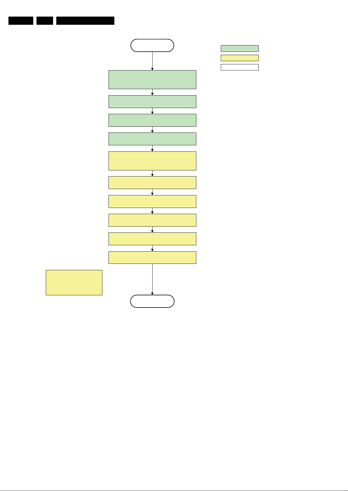
From I_17660_125a.eps From I_17660_125a.eps
EN 19Q529.1E LA 5.
No
3-th try?
Yes
Blink Code as
error code
Reset- system is connected to USB
4to1HDMI Mux and channel decoder.
This cannot be done through the bootscript,
the I/O is on the standby µP
Timing need to be updated if
more mature info is available.
Code =
Layer1: 2
Layer2: 15
Switch AVC PNX85 41
in reset (active low )
Wait 10ms
Switch the NVM reset
line HIGH.
Disable all supply related protections and
switch off the +3V3 +5V DC/DC converter.
Wait 5ms
switch off the remaining DC/DC
converters
Switch Standby
I/O line high.
-reset,
No
Code =
Layer1: 2
Layer2: 53
No
Reset-system is switched HIGH by the
AVC at the end of the bootscript
AVC releases Reset-Ethernet when the
end of the AVC boot-script is detected
Reset-Audio and Audio-Mute-Up are
switched by MIPS code later on in the
Set I²C slave address
of Standby µP to (60h)
RPC start (comm. protocol)
No
image transfer succeeded
No
Enable Alive check mechanism
MIPS reads the wake up reason
Switch on the display in case of a LED backlight
display by sending the TurnOnDisplay(1) (I²C)
command to the PNX5100
Download firmware into the channel
startup process
Bootscript ready
in 1250 ms?
Yes
Flash to Ram
within 30s?
Yes
SW initializatio n
succeeded
within 20s?
Yes
from standby µP.
Initialize audio
decoder
Reset-syst em is switched HIGH by the
AVC at the end of the bootscript
AVC releases Reset-Ethernet when the
end of the AVC boot-script is detected
Reset-Audio and Audio-Mute-Up are
switched by MIPS code later on in the
startup process
Timing needs to
be updated if more
mature info is
available.
Timing needs to be
updated if more
matur e info is
available.
Wait until AVC starts to
communicate
In case of a LED backlight display, a LED DIM panel is
present which is fed by the Vdisplay. To power the LED DIM
Panel, the Vdisplay switch driven by the PNX5100 must be
closed. The display startup sequence is taken care of by the
LED DIM panel.
STi7100AliveFailedError
and generate fast cold reboot
eventually followed by a cold
Alive
polling
NOK
Log SW event
reboot.
Release reset MPEG4 module:
BOLT-ON-IO: High
MPEG4 module will start booting
autonomously.
Wait 3000 ms
POR polling positive?
yes
Start alive IIC polling
mechanism
No
POR polling positive?yes
bootSTi7100PorFailure:
and generate cold boot
Log SW event:
STi7100PorFailure
Wait 200 ms
No
Log HW error
Layer1: 2
Layer2: 38
Enter protection
Third try? No
Yes
Log channel decoder error:
Layer1: 2
Layer2: 37
Downloaded
successfully ?
Yes
initialize tuner, Master IF and channel
decoder
Initiali ze source sele ction
Initialize video processing IC's
initialize AutoTV by triggering CHS AutoTV Init interface
Initialize Ambilight with Lights off.
Semi-Standby
Figure 5-5 “Off” to “Semi Stand-by” flowchart (part 2)
I_17660_125b.eps
140308
EN 20 Q529.1E LA5.
Service Modes, Error Codes, and Fault Finding
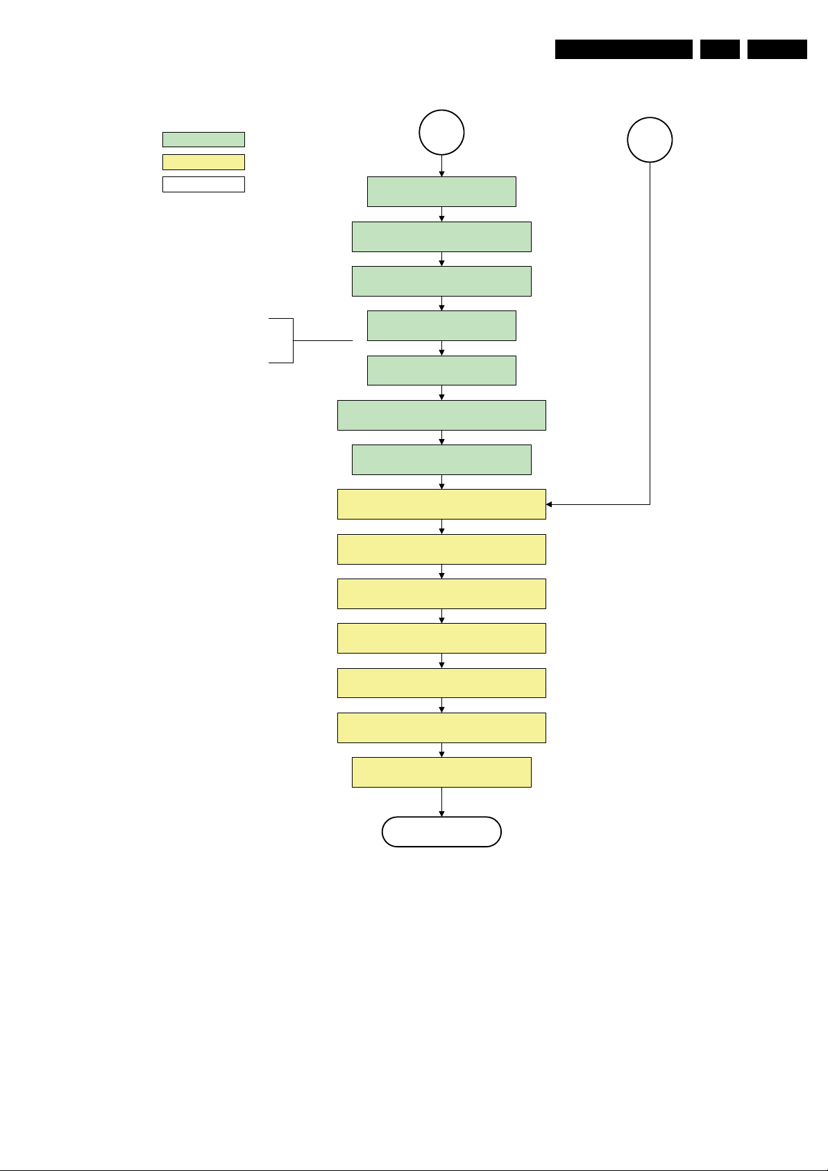
Constraints taken into account:
- Display may only be started when valid LVDS output clock can be delivered by the AVC .
- Between 5 and 50 ms after power is supplied, display should receive valid lvds clock .
- minimum wait time to switch on the lamp after power up is 200ms.
action holder: AVC
action holder: St-by
autonomous action
The assumption here is that a fast toggle (<2s)
can only happen during ON-> SEMI -> ON. In
these states, the AVC is still active and can
provide the 2s delay. If the transition ON-> SEMI-
>STBY -> SEMI -> ON can be made in less th an 2s,
the semi -> stby transition has to be delayed
CPipe already generates a valid output
clock in t he semi -standb y state : display
startup can start immediately when leaving
The timings to be used in
combination with the PanelON
comman d for this specific disp lay
The higher level requirement is that audio and
video should be demuted without transient
effects and that the audio should be demuted
maximum 1s before or at the same time as the
until the requirement is met.
the semi-standby state.
TurnOnDisplay(1) (I²C) command to the PNX5100
unblanking of the video.
Semi Standby
Wait until previous on-state is left more than 2
seconds ago. (to prevent LCD display problems)
Assert RGB video blanking
Switch on the display by sending the
wait 250ms (min. = 200ms)
Switch on LCD backlight
(Lamp-ON)
Wait until valid and stable audio and video , corresponding to
the requested output is delivered by the AVC.
Switch Audio -Reset low and wait 5ms
Release audio mute and wait 100ms before any other audio
handling is done (e.g. volume change)
and audio mute
Initialize audio and video
processing IC's and functions
according needed use case.
The higher level requirement is that the
ambilig ht funct ionality ma y not be sw itched on
before the backlight is turned on in case the
set contains a CE IPB inverter supply.
Figure 5-6 “Semi Stand-by” to “Active” flowchart
unblank the video.
Switch on the Ambilight functionality according the last status
settings.
Active
I_17660_126.eps
140308
Service Modes, Error Codes, and Fault Finding
Constraints taken into account:
- Display may only be started when valid LVDS output clock can be delivered by the AVC .
- Between 5 and 50 ms after power is supplied, display should receive valid lvds clock .
- minimum wait time to switch on the lamp after power up is 200ms.
- To have a reliable operation of the backlight, the backlight should be driven with a PWM duty cycle of 100%
during the first second. Only after this first one or two seconds, the PWM may be set to the required output level
(Note that the PWM output should be present before the backlight is switched on). To minimize the artefacts, the
picture should only be unblanked after these first seconds.
EN 21Q529.1E LA 5.
action holder: AVC
action holder: St-by
autonomous action
The assumption here is that a fast toggle (<2s)
can only happen during ON->SEMI ->ON. In
these states, the AVC is still active and can
provide t he 2s delay. If the t ransition ON -> SEMI-
->STBY-> SEMI -> ON can be made in less than 2s,
the semi -> stby transition has to be delayed
CPipe already generates a valid output
clock in t he semi -standb y state: display
startup can start immediately when leaving
until the requirement is met.
the semi-standby state.
Switch on the display by sending the
TurnOnDisplay(1) (I²C) command to the PNX5100
Switch off the dimming backlight feature, set
the BOOST control to nominal and make sure
Semi Standby
Wait until previous on-state is left more than 2
seconds ago. (to prevent LCD display problems)
Assert RGB video blanking
wait 250ms (min. = 200ms)
PWM output is set to 100%
Switch on LCD backligh t
(Lamp-ON)
and audio mute
Initialize audio and video
processing IC's and functions
according needed use case.
The higher level requirement is that audio and
video should be demuted without transient
effects and that the audio should be demuted
maximum 1s before or at the same time as the
unblanking of the video.
The higher level requirement is that the
ambilig ht funct ionality ma y not be switched on
before the backlight is turned on in case the
set contains a CE IPB inverter supply.
Figure 5-7 “Semi Stand-by” to “Active” flowchart LCD with preheat
Wait until valid and stable audio and video, corresponding to the requested
[the backlight PWM has been on for 1s (internal inverter LPL displays
OR the backlight PWM has been on for 2s (external inverter LPL displays)] .
Release audio mute and wait 100ms before any other audio
handling is done (e.g. volume change)
Restore dimming backlight feature, PWM and BOOST output
Switch on the Ambilight functionality according the last status
output is delivered by the AVC
Switch Audio-Reset low and wait 5ms
AND
and unblank the video.
settings.
Active
I_17660_127.eps
140308
EN 22 Q529.1E LA5.
Service Modes, Error Codes, and Fault Finding
Constraints taken into account:
- Display may only be started when valid LVDS output clock can be delivered by the AVC.
- Between 5 and 50 ms after power is supplied, display should receive valid lvds clock .
- minimum wait time to switch on the lamp after power up is 200ms.
Semi Standby
The assumption here is that a fast toggle (<2s)
can only happen during ON-> SEMI -> ON. In
these states, the AVC is still act ive and can
provide the 2s delay. If the transition ON -> SEMI-
>STBY->SEMI->ON can be made in less than 2s,
the semi -> stby transition has to be delayed
CPipe already generates a valid output
clock in t he semi -standb y state : display
startup can start immediately when leaving
until the requirement is met.
the semi-standby state.
Switch on the display by sending the OUTPUTENABLE (I²C) command to the LED DIM panel
wait 250ms (min. = 200ms)
Switch on LCD backligh t
Wait until previous on-state is left more than 2
seconds ago. (to prevent LCD display problems)
Assert RGB video blanking
TBC in def. spec
(Lamp-ON)
and audio mute
action holder: AVC
action holder: St-by
autonomous action
Initialize audio and video
processing IC's and functions
according needed use case.
The higher level requirement is that audio and
video should be demuted without transient
effects and that the audio should be demuted
maximum 1s before or at the same time as the
ambilig ht funct ionality ma y not be switched on
unblanking of the video.
The higher level requirement is that the
before the backlight is turned on in case the
set contains a CE IPB inverter supply.
Figure 5-8 “Semi Stand-by” to “Active” flowchart (LED backlight)
Wait until valid and stable audio and video , corresponding to
the requested output is delivered by the AVC.
Switch Audio -Reset low and wait 5ms
Release audio mute and wait 100ms before any other audio
handling is done (e.g. volume change)
unblank the video.
Switch on the Ambilight functionality according the last status
settings.
Active
I_17660_128.eps
140308
Service Modes, Error Codes, and Fault Finding
EN 23Q529.1E LA 5.
Active
Mute all sound outputs via softmute
Wait 100ms
Set main amplifier mute (I/O: audio-mute)
Force ext audio outputs to ground
(I/O: audio reset)
And wait 5ms
switch o ff Ambiligh t
Wait until Ambilight has faded out
(fixed wait time of x s)
switch off LCD backlight
Mute all video outputs
action holder: AVC
action holder: St-by
autonomous action
The higher level requirement is that the
backlight may not be switched off before the
ambilight functionality is turned off in case the
set contains a CE IPB inverter supply.
Wait 25 0ms (min. = 200ms)
Switch off the display by sending the
TurnOnDisplay(0) (I²C) command to the PNX5100
Semi Standby
Figure 5-9 “Active” to “Semi Stand-by” flowchart (LCD non DFI)
I_17660_129.eps
140308
EN 24 Q529.1E LA5.
Service Modes, Error Codes, and Fault Finding
Semi Stand by
If ambientlight functionality was used in semi -standby
(lampadaire mode), switch off ambient light
Delay transition until ramping down of ambient light is
transfer Wake up reasons to the Stand by µP.
Switch Memories to self-refresh (this creates a more
stable condition when switching off the power).
Switch AVC system in rese t state
finished. *)
Switch reset-PNX5100 LOW
Switch reset-ST7100 LOW
Switch Reset-Ethernet LOW
Wait 10ms
Switch the NVM reset line HIGH
Switch het WP-Nandflash LOW
action holder: MIPS
action holder: St-by
autonomous action
*) If this is not performed and the set is
switched to standby when the switch off of
the ambilights is still ongoing , the lights will
switch off abruptly when the supply is cut.
Important remark:
release reset audio 10 sec after
entering st andby t o save po wer
Disable all supply related protections and switch off
the DC/DC converters (ENABLE-3V3)
Wait 5ms
Switch OFF all sup plies by switch ing HIGH t he
Standby I/O line
Stand by
Figure 5-10 “Semi Stand-by” to “Stand-by” flowchart
I_17660_130.eps
140308
Service Modes, Error Codes, and Fault Finding
EN 25Q529.1E LA 5.
action holder: MIPS
action holder: St-by
autonomous action
If needed to speed up this transition,
this block could be omitted . This is
depending on the outcome of the
safety investigations .
MP
Log the appropriate err or and
set stand-by flag in NVM
Redefine wake up reasons for protection
state and transfer to stand-by µP.
Switch off LCD lamp supply
Wait 250ms (min. = 200ms)
Switch off LVDS signal
Switch off 12V LCD supply within a time frame of
min. 0.5ms to max. 50ms after LVDS switch off.
Ask stand-by µP to enter protection state
Switch AVC in r eset state
SP
Figure 5-11 “To Protection State” flowchart
5.4 Service Tools
5.4.1 ComPair
Introduction
ComPair (Computer Aided Repair) is a Service tool for Philips
Consumer Electronics products. and offers the following:
1. ComPair helps to quickly get an understanding on how to
repair the chassis in a short and effective way.
2. ComPair allows very detailed diagnostics and is therefore
capable of accurately indicating problem areas. No
knowledge on I
because ComPair takes care of this.
2
C or UART commands is necessary,
Wait 10ms
Switch the NVM r eset line HI GH.
Disable all supply related protections and switch off
the +1V8 and the +3V3 DC/DC converter.
Wait 5ms
Switch OFF all supplies by switching HIGH the
Flash the Protection-LED in order to indicate
Standby I/O line.
protection state* (*): This can be the standby LED or the ON LED
Protection
3. ComPair speeds up the repair time since it can
automatically communicate with the chassis (when the uP
is working) and all repair information is directly available.
4. ComPair features TV software up possibilities.
Specifications
ComPair consists of a Windows based fault finding program
and an interface box between PC and the (defective) product.
The ComPair II interface box is connected to the PC via an
USB cable. For the TV chassis, the ComPair interface box and
the TV communicate via a bi-directional cable via the service
connector(s).
The ComPair fault finding program is able to determine the
problem of the defective television, by a combination of
automatic diagnostics and an interactive question/answer
procedure.
depending on the availability in the set
I_17660_131.eps
140308
EN 26 Q529.1E LA5.
Service Modes, Error Codes, and Fault Finding
How to Connect
This is described in the chassis fault finding database in
ComPair.
TO TV
TO
UART SERVICE
I2C SERVICE
CONNECTOR
CONNECTOR
2
C
I
PC
ComPair II Developed by Philips Brugge
Optional power
5V DC
TO
RS232 /UART
E_06532_036.eps
150208
ComPair II
RC in
Optional
Switch
Power ModeLink/
Activity
HDMI
2
I
C only
UART SERVICE
RC out
TO
CONNECTOR
Multi
function
Figure 5-12 ComPair II interface connection
Caution: It is compulsory to connect the TV to the PC as
shown in the picture above (with the ComPair interface in
between), as the ComPair interface acts as a level shifter. If
one connects the TV directly to the PC (via UART), ICs will be
blown!
How to Order
ComPair II order codes:
• ComPair II interface: 3122 785 91020.
• Software is available via internet:
http://www.atyourservice.ce.philips.com
• ComPair UART interface cable for Q52x.x.
(using 3.5 mm Mini Jack connector): 3104 311 12742.
Note: While encounting problems, contact the local support
desk.
5.4.2 Memory and Audio Test
With this tool you can test the memory of the PNX8541, as well if the PNX5100 is enabled and audio-testing.
What is needed?
– An USB-stick.
– “TESTSCRIPT Q529” (3104 337 05021). Downloadable
from the Philips Service website from the section “Software
for Service only”.
– A ComPair/service cable (3104 311 12742)
Procedure
Create a directory “JETTFILES” under the root of the USB-stick
– Place “MemoryTestPNX8635.bin” and “autojett.bin”
(available in “TESTSCRIPT Q529”) under the directory
“JETTFILES”
– Install the computer program “BOARDTESTLOGGER”
(available in “TESTSCRIPT Q529”) on the PC
– Connect a “ComPair/service”-cable from the service-
connector in the set to the COM1-port of the PC
– Start-up the program “BOARDTESTLOGGER” and select
“COM1”
– Put the USB stick into the TV and startup the TV while
pressing the “i+”-button on a Philips DVD RC6 remote
control (it’s also possible to use a TV remote in “DVD”mode)
– On the PC the memory test is shown now. This is also
visible on the TV screen.
– In “BOARDTESTLOGGER” an option “Send extra UART
command” can be found where you can select “AUD1”.
This command generates hear test tones of 200, 400,
1000, 2000, 3000, 5000, 8000 and 12500Hz.
5.4.3 LVDS Tool
Support of this LVDS Tool has been discontinued.
5.5 Error Codes
5.5.1 Introduction
The error code buffer contains all detected errors since the last
time the buffer was erased. The buffer is written from left to
right, new errors are logged at the left side, and all other errors
shift one position to the right.
When an error occurs, it is added to the list of errors, provided
the list is not full. When an error occurs and the error buffer is
full, then the new error is not added, and the error buffer stays
intact (history is maintained).
To prevent that an occasional error stays in the list forever, the
error is removed from the list after more than 50 hrs. of
operation.
When multiple errors occur (errors occurred within a short time
span), there is a high probability that there is some relation
between them.
New in this chassis is the way errors can be displayed:
• There is a simple blinking LED procedure for board level
repair (home repair) so called LAYER 1 errors next to the
existing errors which are LAYER 2 errors.(see table 5-2
error code overview).
– LAYER 1 errors are one digit errors.
– LAYER 2 errors are 2 digit errors.
• In protection mode.
– From consumer mode: LAYER 1.
– From SDM mode: LAYER 2.
• Fatal errors, if I2C bus is blocked and the set reboots,
CSM and SAM are not selectable.
– From consumer mode: LAYER 1.
– From SDM mode: LAYER 2.
Important remark:
For all errors detected by MIPS which are fatal =>
rebooting of the TV set (reboot starts after LAYER error
1 blinking), one should short the solder paths at startup from the power OFF state by mains interruption and
not via the power button to trigger the SDM via the
hardware pins.
• In CSM mode
– When entering CSM: error LAYER 1 will be displayed
by blinking LED. Only the latest error is shown.
• In SDM mode
– When SDM is entered via Remote Control code or the
hardware pins, LAYER 2 is displayed via blinking LED.
• In the ON state
– In “Display error mode”, set with the RC commands
“mute_06250X _OK” LAYER 2 errors are displayed via
blinking LED.
• Error display on screen.
– In CSM no error codes are displayed on screen.
– In SAM the complete error list is shown.
Basically there are three kinds of errors:
• Errors detected by the Stand-by software which lead to
protection. These errors will always lead to protection and
an automatic start of the blinking LED LAYER error 1.
(see section “5.6 The Blinking LED Procedure”).
• Errors detected by the Stand-by software which not
lead to protection. In this case the front LED should blink
the involved error. See also section “5.5 Error Codes, 5.5.4
Error Buffer, Extra Info”. Note that it can take up several
minutes before the TV starts blinking the error (e.g. LAYER
error 1 = 2, LAYER error 2 = 15 or 53).

Service Modes, Error Codes, and Fault Finding
• Errors detected by main software (MIPS). In this case
the error will be logged into the error buffer and can be read
out via ComPair, via blinking LED method LAYER error 12, or in case picture is visible, via SAM.
5.5.2 How to Read the Error Buffer
Use one of the following methods:
• On screen via the SAM (only when a picture is visible).
E.g.:
– 00 00 00 00 00: No errors detected
– 23 00 00 00 00: Error code 23 is the last and only
detected error.
– 37 23 00 00 00: Error code 23 was first detected and
error code 37 is the last detected error.
– Note that no protection errors can be logged in the
error buffer.
• Via the blinking LED procedure. See section 5.5.3 How to
Clear the Error Buffer.
•Via ComPair.
5.5.3 How to Clear the Error Buffer
Use one of the following methods:
• By activation of the “RESET ERROR BUFFER” command
in the SAM menu.
• With a normal RC, key in sequence “MUTE” followed by
“062599” and “OK”.
• If the content of the error buffer has not changed for 50+
hours, it resets automatically.
EN 27Q529.1E LA 5.
5.5.4 Error Buffer
In case of non-intermittent faults, clear the error buffer before
starting to repair (before clearing the buffer, write down the
content, as this history can give significant information). This to
ensure that old error codes are no longer present.
If possible, check the entire contents of the error buffer. In
some situations, an error code is only the result of another error
code and not the actual cause (e.g. a fault in the protection
detection circuitry can also lead to a protection).
There are several mechanisms of error detection:
• Via error bits in the status registers of ICs.
• Via polling on I/O pins going to the stand-by processor.
• Via sensing of analog values on the stand-by processor or
the PNX8541.
• Via a “not acknowledge” of an I
Take notice that some errors need several minutes before they
start blinking or before they will be logged. So in case of
problems wait 2 minutes from start-up onwards, and then
check if the front LED is blinking or if an error is logged.
2
C communication.
EN 28 Q529.1E LA5.
Table 5-2 Error code overview
Service Modes, Error Codes, and Fault Finding
Description Layer 1 Layer 2
2
C3 2 13 MIPS E BL / EB SCL/D-SSB SSB
I
2
C4 5 14 MIPS E BL / EB SCL/D-DISP Display (LED back light only)
I
by
PNX doesn’t boot (HW cause) 2 15 Stby µP E BL PNX8541 I
Monitored
Error/
Error Buffer/
Prot
Blinking LED Device Defective Board
2
C blocked SSB
12V 3 16 Stby µP P BL / Supply
1V2, 3V3, 5V to low 2 18 Stby µP P BL / SSB
1V2 or Class D 2 19 Stby µP P BL / SSB
3V3/5V DCDC to high 2 11 Stby µP P BL / SSB
PNX 5100 2 21 MIPS E EB PNX5100 SSB
HDMI mux 2 23 MIPS E EB AD8197A SSB
2
C switch 2 24 MIPS E EB PCA9540 SSB
I
Master IF 2 26 MIPS E EB TDA9898 SSB
FPGA Ambilight 2 28 MIPS E EB / SSB
Tuner 2 34 MIPS E EB UV1783S/TD1716 SSB
Channel Decoder DVB-T 2 37 MIPS E EB TDA10048 SSB
ST7100 2 38 MIPS E EB ST7100 SSB
MHP 6 39 MIPS E EB / MHP module
Fan I2C expander 7 41 MIPS E EB PCA9533 FAN module
T° sensor 7 42 MIPS E EB LM 75 T° sensor
FAN 1 7 43 MIPS E EB FAN
FAN 2 7 44 MIPS E EB FAN
main NVM 2 / MIPS E X STM24C128 SSB
Channel decoder DVB-C 2 48 MIPS E EB TDA 10023 SSB
PNX doesn’t boot (SW cause) 2 53 Stby µP E BL PNX8541 SSB
Display (only LED back light) 5 64 MIPS E BL / EB Display
Extra Info
• Rebooting. When a TV is constantly rebooting due to
internal problems, most of the time no errors will be logged
or blinked. This rebooting can be recognized via a ComPair
interface and Hyperterminal (for Hyperterminal settings,
see section “5.8 Fault Finding and Repair Tips, 5.8.6
Logging). It’s shown that the loggings which are generated
by the main software keep continuing. In this case
diagnose has to be done via ComPair.
• Error 11 (3V3/5V too high). This protection can occur
during start up (LAYER error 1 = 2). Be careful to overrule
this protection via SDM for the reason supply related
devices can be possibly destroyed here.
• Error 13 (I
2
C bus 3 blocked). At the time of release of this
manual, this error was not working as expected. Current
situation: when this error occurs, the TV will constantly
reboot due to the blocked bus. The best way for further
diagnosis here, is to use ComPair.
• Error 15 (PNX8541 doesn’t boot). Indicates that the main
processor was not able to read his bootscript. This error will
point to a hardware problem around the PNX8541
(supplies not OK, PNX 8541 completely dead, I
between PNX and Stand-by Processor broken, etc...).
When error 15 occurs it is also possible that I
blocked (NVM). I
2
C2 can be indicated in the schematics as
2
C link
2
C2 bus is
follows: SCL-UP-MIPS, SDA-UP-MIPS, SCL-2 or SDA-2.
Other root causes for this error can be due to hardware
problems with : NVM PNX5100, PNX5100 itself, DDR’s.
• Error 16 (12V). This voltage is made in the power supply
and results in protection (LAYER error 1 = 3) in case of
absence. When SDM is activated we see blinking LED
LAYER error 2 = 16.
• Error 18 (1V2-3V3-5V too low). All these supplies are
generated by the DC/DC supply on the SSB. If one of these
supplies is too low, protection occurs and blinking LED
LAYER error 1 = 2 will be displayed automatically. In SDM
this gives LAYER error 2 = 18.
• Error 19 (1V2 or class D). This is an combination of two
detections:
– If one of the 1V2 supplies is too high or too low in the
start up procedure the supply fault becomes low.
– If a DC voltage occurs on the output of the Class D
amplifier the supply fault becomes low. Be careful to
overrule this protection via SDM, check audio part first
before apply. In case one of the speakers is not
connected, the protection can also be triggered.
• Error 21 (PNX 5100). At the time of release of this manual,
this error was not working as expected. Current situation:
when this error occurs, the TV will constantly reboot. This
rebooting can be recognized via a ComPair interface and
Hyperterminal (for Hyperterminal settings, see section “5.8
Fault Finding and Repair Tips, 5.8.6 Logging”). It is shown
that the loggings which are generated by the main software
keep continuing. The best way for further diagnosis here, is
to use ComPair.
• Error 21 (PNX 5100). At the time of release of this manual,
this error was not working as expected. Current situation:
when there is no I
after startup (power off by disconnection of the mains
cord), LAYER error 2 will blink continuously via the blinking
LED procedure in SDM. (startup the TV with the solder
paths short to activate SDM).
• Error 23 (HDMI). When there is no I
towards the HDMI mux after start up, LAYER error 2 = 23
will be logged and displayed via the blinking LED
procedure if SDM is switched on.
• Error 26 (Master IF). When there is no I
towards the Master IF after start up, LAYER error 2 = 26
will be logged and displayed via the blinking LED
procedure when SDM is switched on.
• Error 28 (FPGA ambilight). When there is no I
communication towards the FPGA ambilight after start up,
LAYER error 2 = 28 will be logged and displayed via the
blinking LED procedure if SDM is switched on. Note that it
can take up several minutes before the TV starts blinking
LAYER error 1 = 2 in CSM or in SDM, LAYER error 2 = 28.
• Error 34 (Tuner). When there is no I
towards the tuner after start up, LAYER error 2 = 34 will be
logged and displayed via the blinking LED procedure when SDM is switched on.
2
C communication towards the PNX5100
2
C communication
2
C communication
2
C
2
C communication

Service Modes, Error Codes, and Fault Finding
EN 29Q529.1E LA 5.
• Error 37 (Channel decoder DVBT). When there is no I2C
communication towards the DVBT channel decoder after
start up, LAYER error 2 = 37 will be logged and displayed
via the blinking LED procedure if SDM is switched on.
• Error 38 (STI7100). When there is no I
2
C communication
towards the STI7100 after startup (power off by
disconnection of the mains cord), LAYER error 2 = 38 will
be logged and displayed via the blinking LED procedure in
SDM (startup the TV with the solder paths short to activate
SDM). Remark : if the error occurs during the ON state, the
TV will constantly reboot and no LED blinking will be
displayed. This rebooting can be recognized via a ComPair
interface and Hyperterminal (for Hyperterminal settings,
see section “5.8 Fault Finding and Repair Tips, 5.8.6
Logging”). It is shown that the loggings which are
generated by the main software keep continuing. Check in
the logging for keywords like e.g. “Device error 38”.
• Main NVM. When there is no I
2
C communication towards
the main NVM, LAYER error 1 = 2 will be displayed via the
blinking LED procedure. In SDM, LAYER error 2 can be 19.
Check the logging for keywords like “I
2
C bus blocked”.
• Error 48 (Channel decoder DVBC). When there is no I
communication towards the DVBC channel decoder after
start up, LAYER error 2 = 48 will be logged and displayed
via the blinking LED procedure while SDM is active.
• Error 53. This error will indicate that the PNX8541 has
read his bootscript (when this would have failed, error 15
would blink) but initialization was never completed because
of hardware problems (NAND flash, ...) or software
initialization problems. Possible cause could be that there
is no valid software loaded (try to upgrade to the latest main
software version). Note that it can take up to 2 minutes
before the TV starts blinking LAYER error 1 = 2 or in SDM,
LAYER error 2 = 53.
5.6 The Blinking LED Procedure
5.6.1 Introduction
The blinking LED procedure can be split up into two situations:
• Blinking LED procedure LAYER error 1. In this case the
error is automatically blinked when the TV is put in CSM.
This will be only one digit error, namely the one that is
referring to the defective board (see table “Table 5-2 Error
code overview”) which causes the failure of the TV. This
approach will especially be used for home repair and call
centres. The aim here is to have service diagnosis from a
distance.
• Blinking LED procedure LAYER error 2. Via this procedure,
the contents of the error buffer can be made visible via the
front LED. In this case the error contains 2 digits (see table
“Table 5-2 Error code overview”) and will be displayed
when SDM (hardware pins) is activated. This is especially
useful for fault finding and gives more details regarding the
failure of the defective board.
Important remark:
For all errors detected by MIPS which are fatal =>
rebooting of the TV set (reboot starts after LAYER error 1
blinking), one should short the solder paths at start-up from
the power OFF state by mains interruption and not via the
power button to trigger the SDM via the hardware pins.
Example: Error 12 8 6 0 0.
After activation of the SDM, the front LED will show:
1. One long blink of 750 ms (which is an indication of the
decimal digit) followed by a pause of 1.5 s
2. Two short blinks of 250 ms followed by a pause of 3 s
3. Eight short blinks followed by a pause of 3 s
4. Six short blinks followed by a pause of 3 s
5. One long blink of 3 s to finish the sequence
6. The sequence starts again.
5.6.2 How to Activate
Use one of the following methods:
• Activate the CSM. The blinking front LED will show only
the latest layer error 1, this works in “normal operation”
mode or automatically when the error/protection is
monitored by the standby processor. At the time of this
release, this layer error 1 blinking was not working as
expected.
2
C
In case no picture is shown and there is no LED blinking, n
read the logging to detect whether “error devices” are
mentioned. (see section “5.8 Fault Finding and Repair
Tips, 5.8.6 Logging”).
• Activate the SDM. The blinking front LED will show the
entire contents of the layer error 2 buffer, this works in
“normal operation” mode or when SDM (via hardware pins)
is activated when the tv set is in protection.
Important remark:
For all errors detected by MIPS which are fatal =>
rebooting of the TV set (reboot starts after LAYER error 1
blinking), one should short the solder paths at start-up from
the power OFF state by mains interruption and not via the
power button to trigger the SDM via the hardware pins.
• Transmit the commands “MUTE” - “062500” - “OK”
with a normal RC. The complete error buffer is shown.
Take notice that it takes some seconds before the blinking
LED starts.
• Transmit the commands “MUTE” - “06250x” - “OK”
with a normal RC (where “x” is a number between 1
and 5). When x = 1 the last detected error is shown, x = 2
the second last error, etc.... Take notice that it takes some
seconds before the blinking LED starts.
5.7 Protections
5.7.1 Software Protections
Most of the protections and errors use either the stand-by
microprocessor or the MIPS controller as detection device.
Since in these cases, checking of observers, polling of ADCs,
and filtering of input values are all heavily software based,
these protections are referred to as software protections.
There are several types of software related protections, solving
a variety of fault conditions:
• Protections related to supplies: check of the 12V, +5V,
+3V3 and 1V2.
• Protections related to breakdown of the safety check
mechanism. E.g. since the protection detections are done
by means of software, failing of the software will have to
initiate a protection mode since safety cannot be
guaranteed any more.
When one of the blinking LED procedures is activated, the front
LED will show (blink) the contents of the error-buffer. Error
codes greater then 10 are shown as follows:
1. “n” long blinks (where “n” = 1 to 9) indicating decimal digit
2. A pause of 1.5 s
3. “n” short blinks (where “n”= 1 to 9)
4. A pause of approximately 3 s,
5. When all the error codes are displayed, the sequence
finishes with a LED blink of 3 s
6. The sequence starts again.
Remark on the Supply Errors
The detection of a supply dip or supply loss during the normal
playing of the set does not lead to a protection, but to a cold
reboot of the set. If the supply is still missing after the reboot,
the TV will go to protection.
Protections during Start-up
During TV start-up, some voltages and IC observers are
actively monitored to be able to optimise the start-up speed,
and to assure good operation of all components. If these

EN 30 Q529.1E LA5.
Service Modes, Error Codes, and Fault Finding
monitors do not respond in a defined way, this indicates a
malfunction of the system and leads to a protection. As the
observers are only used during start-up, they are described in
the start-up flow in detail (see section “5.3 Stepwise Start-up”).
5.7.2 Hardware Protections
The only real hardware protection in this chassis appears in
case of an audio problem e.g. DC voltage on the speakers. The
audio protection circuit pulls the “supply-fault” low and the tv set
will blink LAYER error 1 = 2 or in SDM, LAYER error 2 = 19. Be
very careful to overrule this protection via SDM (not to cause
damage to the Class D audio amplifier). Check audio part first
before activating via SDM. In case one of the speakers is not
connected, the protection can also be triggered.
Repair Tips
• It is also possible that the set has an audio DC protection
because of an interruption in one or both speakers (the DC
voltage that is still on the circuit cannot disappear through
the speakers). Caution: (Dis)connecting the speakers
during the ON state of the TV can damage the audio
amplifier.
5.7.3 Important remark regarding the blinking LED indication
As for the blinking LED indication, the blinking led of error
layer 1 displaying can be switched off by pushing the power
button on the keyboard.
This condition is not valid after the set was unpowered (via
mains interruption). The blinking LED starts again and can only
be switched off by unplugging the mains connection.
This can be explained by the fact that the MIPS can not load
the keyboard functionality from software during the start-up and
doesn’t recognizes the keyboard commands at this time.
5.8 Fault Finding and Repair Tips
Read also section “5.5 Error Codes, 5.5.4 Error Buffer, Extra
Info”.
Caution: For the whole platform the speaker connections are
grounded on -12 V level. During service measurements with
earth grounded equipment like e.g. scope, great risk of using
the speaker terminal connections for earth ground is currently
present. One will short circuit the -12 V to earth ground in that
way and will causes damage of the supply/audio part!
5.8.1 Ambilight
Due to degeneration process of the AmbiLights, there can be a
difference in the colour and/or light output of the spare
ambilight module in comparison with the originals ones
contained in the TV set. Via ComPair the light output can be
adjusted.
5.8.2 Audio Amplifier
The Class D-IC 7D10 has a powerpad for cooling. When the IC
is replaced it must be ensured that the powerpad is very well
pushed to the PCB while the solder is still liquid. This is needed
to insure that the cooling is guaranteed, otherwise the Class DIC could break down in short time.
5.8.3 CSM
When CSM is activated and there is a USB stick connected to
the TV, the software will dump the complete CSM content to the
USB stick. The file (Csm.txt) will be saved in the root of the USB
stick. If this mechanism works it can be concluded that a large
part of the operating system is already working (MIPS, USB...)
5.8.4 DC/DC Converter
Introduction
The onboard supply consists of 5 DC/DC converters and 7
linear stabilizers. The DC/DC converters have all +12V input
voltage and deliver:
1. +1V2-PNX8541 supply voltage, stabilized close to
PNX8541 chip.
2. +1V2-PNX5100 supply voltage, stabilized close to
PNX5100 chip.
3. +3V3 (overall 3.3 V for onboard IC’s).
4. +5V for USB and Conditional Access Interface and +5V5TUN tuner stabilizer.
5. +33VTUN for analog only tuners (AP diversity).
The linear stabilizers are providing:
1. +1V supply voltage (out of +1V2-PNX8541), stabilized
close to ST7101 chip (MPEG4 diversity).
2. +1V8-PNX5100.
3. +1V8-PNX8541 (reserved because +1V8-PNX5100 used
also for DDR2 interface of PNX8541 via 5FB0).
4. +2V5 (MPEG4 diversity).
5. +1V2-STANDBY (out of +3V3-STANDBY).
6. +5V-TUN (out of +5V5-TUN).
7. +3V3-STANDBY (out of +12V, reserved).
+3V3-STANDY and +1V2-STANDBY are permanent voltages.
Supply voltages +1V2-PNX8541, +1V2-PNX5100 and +1V are
started immediately when +12V incoming voltage is available
(+12V is enabled by STANDBY signal, active low). Supply
voltages +3V3, 2V5, +1V8-PNX5100, +1V8-PNX8541, +5V
and +5V-TUN are switched-on directly by signal ENABLE-3V3
(active low) when +12V and previous mentioned voltages are
all available.
Debugging
The best way to find a failure in the DC/DC converters is to
check their starting-up sequence at power-on via the mains
cord, presuming that the standby microprocessor and the
external supply are operational. Take STANDBY signal highto-low transition as reference.
When +12V rises above 10V then +1V2-PNX8541, +1V2PNX5100 and +1V are started immediately. Then, after
ENABLE-3V3 goes low, all the other supply voltages should
rise within 10 ms. Boost voltages should be OK when +1V2PNX8541, +1V2-PNX5100 are available (FU07 and FU8A,
around 19V).
SUPPLY-FAULT signal should be high when all supply
voltages are started-up.
Tips
• Usually, when supply voltage is short-circuited to GND, the
corresponding DC/DC converter is making audible noise.
• The drop voltage across resistors 3U70 and 3U3T is
100 mV to 2000 mV.
• Defective (in short-circuit) power MOS-FET’s lead usually
to their controller IC broken; if one or more high-side MOSFET’s (7U05, 7U08, 7U0D-1 or 7U0H-1) is broken then the
platform can be heavily damaged if started in SDM-mode
(SUPPLY-FAULT signal is then ignored, while higher than
normal supplies will be generated).
• The +33VTUN generator circuit (7U0P + 7U0Q +
surrounding components) has low output current
capability. In case of too low or no output voltage check
transistor 7U0P (gate voltage pulses of about 10 V
amplitude and drain voltage pulses of about 35 V
amplitude) and the load (not more than 4.5 mA).
• High output ripple voltage of DC/DC converters can be
caused by defective (cracked or bad soldered) ceramic
capacitors in the feedback (DC or AC) input or output
filtering.
Loading...