


 Loading...
Philips PXAS37KBBE, PXAS37KFA, PXAS37KFBE, PXAS30KBA, PXAS30KFA Datasheet
...INTEGRATED CIRCUITS
XA-S3
XA 16-bit microcontroller
32 K/1 K OTP/ROM/ROMless, 8-channel 8-bit A/D, low voltage (2.7 V±5.5 V), I2C, 2 UARTs,
16 MB address range
Preliminary specification |
2000 Dec 01 |
Supersedes data of 2000 Aug 22 |
|
P s
on o s

Philips Semiconductors |
Preliminary specification |
|
|
|
|
|
|
|
XA 16-bit microcontroller
32 K/1 K OTP/ROM/ROMless, 8-channel 8-bit A/D, low voltage (2.7 V±5.5 V), I2C, 2 UARTs, 16 MB address range
XA-S3
GENERAL DESCRIPTION
The XA-S3 device is a member of Philips Semiconductors' XA (eXtended Architecture) family of high performance 16-bit single-chip microcontrollers.
The XA-S3 device combines many powerful peripherals on one chip. With its high performance A/D converter, timers/counters, watchdog, Programmable Counter Array (PCA), I2C interface, dual
UARTs, and multiple general purpose I/O ports, it is suited for general multipurpose high performance embedded control functions.
Specific features of the XA-S3
•2.7 V to 5.5 V operation.
•32 K bytes of on-chip EPROM/ROM program memory.
•1024 bytes of on-chip data RAM.
•Supports off-chip addressing up to 16 megabytes (24 address lines). A clock output reference is added to simplify external bus interfacing.
•High performance 8-channel 8-bit A/D converter with automatic channel scan and repeated read functions. Completes a conversion in 4.46 microseconds at 30 MHz. Alternate operating mode allows 10-bit conversion results.
•Three standard counter/timers with enhanced features. All timers have a toggle output capability.
•Watchdog timer.
•5-channel 16-bit Programmable Counter Array (PCA).
•I2C-bus serial I/O port with byte-oriented master and slave functions.
•Two enhanced UARTs with independent baud rates.
•Seven software interrupts.
•Active low reset output pin indicates all reset occurrences
(external reset, watchdog reset and the RESET instruction). A reset source register allows program determination of the cause of
the most recent reset.
•50 I/O pins, each with 4 programmable output configurations.
•30 MHz operating frequency at 2.7±5.5 V VDD.
•Power saving operating modes: Idle and Power-down. Wake-up from power-down via an external interrupt is supported.
•68-pin PLCC and 80-pin PQFP packages.
ORDERING INFORMATION
ROMless |
ROM |
EPROM |
|
TEMPERATURE RANGE (°C) |
FREQ. |
DRAWING |
|
|
|
|
AND PACKAGE |
(MHz) |
NUMBER |
|
|
|
|
|
|
|
PXAS30KBA |
PXAS33KBA |
PXAS37KBA |
OTP |
0 to +70, Commercial |
30 |
SOT188-3 |
|
|
|
|
68-pin Plastic Leaded Chip Carrier |
|
|
|
|
|
|
|
|
|
PXAS30KBBE |
PXAS33KBBE |
PXAS37KBBE |
OTP |
0 to +70, Commercial |
30 |
SOT315-1 |
|
|
|
|
80-pin Plastic Low Profile Quad Flat Pack |
|
|
|
|
|
|
|
|
|
PXAS30KFA |
PXAS33KFA |
PXAS37KFA |
OTP |
±40°C to +85°C, Industrial 68-pin Plastic |
30 |
SOT188-3 |
|
|
|
|
Leaded Chip Carrier |
|
|
|
|
|
|
|
|
|
PXAS30KFBE |
PXAS33KFBE |
PXAS37KFBE |
OTP |
±40°C to +85°C, Industrial 80-pin Plastic Low |
30 |
SOT315-1 |
|
|
|
|
Profile Quad Flat Pack |
|
|
|
|
|
|
|
|
|
2000 Dec 01 |
2 |

Philips Semiconductors |
Preliminary specification |
XA 16-bit microcontroller
32 K/1 K OTP/ROM/ROMless, 8-channel 8-bit A/D, low voltage (2.7 V±5.5 V), I2C, 2 UARTs, 16 MB address range
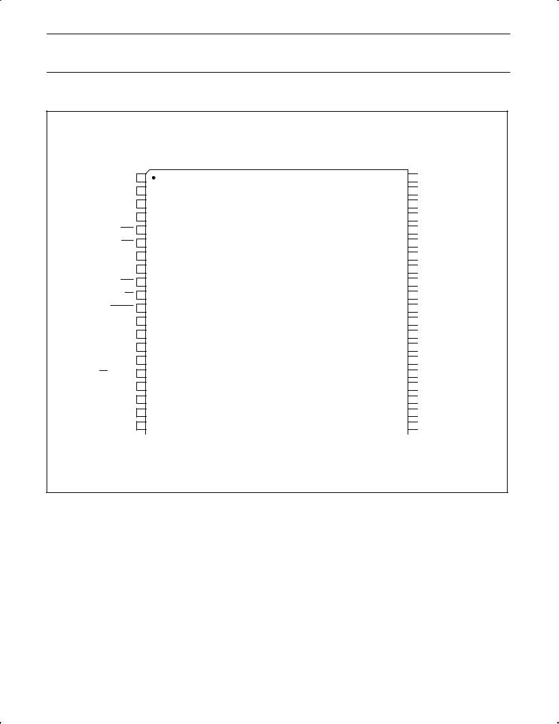
PIN CONFIGURATIONS
68-pin PLCC package
XA-S3
|
|
|
|
|
|
|
|
|
|
|
P4.6/A20 |
P4.5/CEX4 |
|
P4.4/CEX3 |
P4.3/CEX2 |
|
P4.2/CEX1 |
P4.1/CEX0 |
P4.0/ECI |
V |
V |
XTAL1 |
|
XTAL2 |
P2.7/A19D15 |
|
P2.6/A18D14 |
P2.5/A17D13 |
P2.4/A16D12 |
|
P2.3/A15D11 |
P2.2/A14D10 |
|
|
|
|
|
|
|
|||||||||||||
|
|
|
|
|
|
|
|
|
|
|
|
|
|
|
|
|
|
|
|
|
|
|
|
|
DD |
SS |
|
|
|
|
|
|
|
|
|
|
|
|
|
|
|
|
|
|
|
|
|
|
|
|
||
|
|
|
|
|
|
|
|
|
|
|
|
|
|
|
|
|
|
|
|
|
|
|
|
|
|
|
|
|
|
|
|
|
|
|
|
|
|
|
|
|
|
|
|
|
|
|
|
|
|
|
|
|
|
|
|
|
|
|
|
|
|
|
9 |
|
8 |
|
7 |
|
6 |
|
5 |
|
4 |
|
3 |
|
2 |
|
1 |
|
68 |
|
67 |
|
66 |
|
65 |
|
64 |
|
63 |
|
62 |
|
61 |
|
|
|
|
|
|
|
|
|
|
|
|
|
|
|
|
|
|
|
|
|
|
|
|
|
|
|
|
|
|
|
|
|
|
|
|
|
|
|
|
|
|
|
|
|
|
|
|
|
|
|
|
|
|
|
|
|
|
|
|
|
|
|
|
|
|
|
|
|
|
|
|
|
|
|
|
|
|
|
|
|
|
|
|
|
|
|
|
|
|
|
|
|
|
|
|
|
|
|
|
|
|
|
|
|
|
|
|
|
|
|
|
|
|
|
|
|
|
P4.7/A21 |
10 |
|
|
|
|
|
|
|
|
|
|
|
|
|
|
|
|
|
|
|
|
|
|
|
|
|
|
|
|
|
|
|
|
|
|
|
60 |
P2.1/A13D9 |
||||||||||||
|
|
|
|
|
|
|
|
|
|
|
|
|
|
|
|
|
|
|
|
|
|
|
|
|
|
|
|
|
|
|
|
|
|
|
|
|
|
|
|
|
|
|
|
|
|
|
|
|
|
|
|
|
|
|
|
|
|
|
|
|
|
|
|
|
|
|
|
|
|
|
|
|
|
|
|
|
|
|
|
|
|
|
|
|
|
|
|
|
|
|
|
|
|
|
|
|
|
|
|
|
|
|
|
|
|
|
P3.0/RxD0 |
11 |
|
|
|
|
|
|
|
|
|
|
|
|
|
|
|
|
|
|
|
|
|
|
|
|
|
|
|
|
|
|
|
|
|
|
|
59 |
P2.0/A12D8 |
|||||||||||||
|
|
|
|
|
|
|
|
|
|
|
|
|
|
|
|
|
|
|
|
|
|
|
|
|
|
|
|
|
|
|
|
|
|
|
|
|
|
|
|
|
|
|
|
|
|
|
|
|
|
|
|
|
|
|
|
|
|
|
|
|
|
|
|
|
|
|
|
|
|
|
|
|
|
|
|
|
|
|
|
|
|
|
|
|
|
|
|
|
|
|
|
|
|
|
|
|
|
|
|
|
|
|
|
|
|
|
|
P3.1/TxD0 |
12 |
|
|
|
|
|
|
|
|
|
|
|
|
|
|
|
|
|
|
|
|
|
|
|
|
|
|
|
|
|
|
|
|
|
|
|
58 |
P0.7/A11D7 |
||||||||||||
|
|
|
|
|
|
|
|
|
|
|
|
|
|
|
|
|
|
|
|
|
|
|
|
|
|
|
|
|
|
|
|
|
|
|
|
|
|
|
|
|
|
|
|
|
|
|
|
|
|
|
|
|
|
|
|
|
|
|
|
|
|
|
|
|
|
|
|
|
|
|
|
|
|
|
|
|
|
|
|
|
|
|
|
|
|
|
|
|
|
|
|
|
|
|
|
|
|
|
|
|
|
|
|
|
|
|
|
P3.2/INT0 |
|
13 |
|
|
|
|
|
|
|
|
|
|
|
|
|
|
|
|
|
|
|
|
|
|
|
|
|
|
|
|
|
|
|
|
|
|
|
57 |
P0.6/A10D6 |
|||||||||||
|
|
|
|
|
|
|
|
|
|
|
|
|
|
|
|
|
|
|
|
|
|
|
|
|
|
|
|
|
|
|
|
|
|
|
|
|
|
|
|
|
|
|
|
|
|
|
|
|
|
|
|
|
|
|
P3.3/INT1 |
|
14 |
|
|
|
|
|
|
|
|
|
|
|
|
|
|
|
|
|
|
|
|
|
|
|
|
|
|
|
|
|
|
|
|
|
|
|
56 |
P0.5/A9D5 |
|||||||||||
|
|
|
P3.4/T0 |
|
|
|
|
|
|
|
|
|
|
|
|
|
|
|
|
|
|
|
|
|
|
|
|
|
|
|
|
|
|
|
|
|
|
|
|
|
VSS |
|||||||||||
|
|
|
15 |
|
|
|
|
|
|
|
|
|
|
|
|
|
|
|
|
|
|
|
|
|
|
|
|
|
|
|
|
|
|
|
|
|
|
|
55 |
|||||||||||||
P3.5/T1/BUSW |
|
|
|
|
|
|
|
|
|
|
|
|
|
|
|
|
|
|
|
|
|
|
|
|
|
|
|
|
|
|
|
|
|
|
|
|
|
|
|
|
|
|
|
|
||||||||
16 |
|
|
|
|
|
|
|
|
|
|
|
|
|
|
|
|
|
|
|
|
|
|
|
|
|
|
|
|
|
|
|
|
|
|
|
54 |
VDD |
|||||||||||||||
|
|
|
|
|
|
|
|
|
|
|
|
|
|
|
|
|
|
|
|
|
|
|
|
|
|
|
|
|
|
|
|
|
|
|
|
|
|
|
|
|
|
|
|
|
|
P0.4/A8D4 |
||||||
|
|
P3.6/WRL |
|
17 |
|
|
|
|
|
|
|
|
|
|
|
|
|
|
|
|
|
|
|
|
|
|
|
|
|
|
|
|
|
|
|
|
|
|
|
53 |
||||||||||||
|
|
|
|
|
|
|
|
|
|
|
|
|
|
|
|
|
|
PLASTIC LEADED CHIP CARRIER |
|
|
|
|
|
|
|
|
|
P0.3/A7D3 |
||||||||||||||||||||||||
|
|
|
P3.7/RD |
|
18 |
|
|
|
|
|
|
|
|
|
|
|
|
|
|
|
|
52 |
||||||||||||||||||||||||||||||
|
|
|
|
|
|
|
|
|
|
|
|
|
|
|
|
|
|
|
|
|
|
|
|
|
|
|
|
|
|
|
|
|
|
|
|
|
|
|
|
|
|
|
|
|
|
|
|
|
|
|
|
|
|
|
|
RSTOUT |
|
19 |
|
|
|
|
|
|
|
|
|
|
|
|
|
|
|
|
|
|
|
|
|
|
|
|
|
|
|
|
|
|
|
|
|
|
|
51 |
|
P0.2/A6D2 |
|||||||||
|
|
|
|
|
|
|
|
|
|
|
|
|
|
|
|
|
|
|
|
|
|
|
|
|
|
|
|
|
|
|
|
|
|
|
|
|
|
|
|
|
|
|
|
|
|
|
|
|
|
|
|
|
|
|
|
|
VSS |
20 |
|
|
|
|
|
|
|
|
|
|
|
|
|
|
|
|
|
|
|
|
|
|
|
|
|
|
|
|
|
|
|
|
|
|
|
50 |
|
RST |
|
|
|
|
|||||
|
|
|
|
|
|
|
|
|
|
|
|
|
|
|
|
|
|
|
|
|
|
|
|
|
|
|
|
|
|
|
|
|
|
|
|
|
|
|
|
|
|
|
|
|
|
|
|
|
|
|
|
|
|
|
|
|
VDD |
21 |
|
|
|
|
|
|
|
|
|
|
|
|
|
|
|
|
|
|
|
|
|
|
|
|
|
|
|
|
|
|
|
|
|
|
|
49 |
|
CLKOUT |
|||||||||
|
|
|
|
|
|
|
|
|
|
|
|
|
|
|
|
|
|
|
|
|
|
|
|
|
|
|
|
|
|
|
|
|
|
|
|
|
|
|
|
|
|
|
|
|
|
|
|
|
|
|
|
|
|
EA/WAIT/VPP |
22 |
|
|
|
|
|
|
|
|
|
|
|
|
|
|
|
|
|
|
|
|
|
|
|
|
|
|
|
|
|
|
|
|
|
|
|
48 |
|
|
PSEN |
|
|
|||||||||
|
|
P5.0/AD0 |
|
|
|
|
|
|
|
|
|
|
|
|
|
|
|
|
|
|
|
|
|
|
|
|
|
|
|
|
|
|
|
|
|
|
|
|
|
|
|
|
|
|
|
|
||||||
|
|
23 |
|
|
|
|
|
|
|
|
|
|
|
|
|
|
|
|
|
|
|
|
|
|
|
|
|
|
|
|
|
|
|
|
|
|
|
47 |
|
ALE/PROG |
|
|||||||||||
|
|
P5.1/AD1 |
|
|
|
|
|
|
|
|
|
|
|
|
|
|
|
|
|
|
|
|
|
|
|
|
|
|
|
|
|
|
|
|
|
|
|
|
|
|
P0.1/A5D1 |
|||||||||||
|
|
24 |
|
|
|
|
|
|
|
|
|
|
|
|
|
|
|
|
|
|
|
|
|
|
|
|
|
|
|
|
|
|
|
|
|
|
|
46 |
|
|||||||||||||
|
|
P5.2/AD2 |
|
|
|
|
|
|
|
|
|
|
|
|
|
|
|
|
|
|
|
|
|
|
|
|
|
|
|
|
|
|
|
|
|
|
|
|
|
P0.0/A4D0 |
||||||||||||
|
|
|
|
|
|
|
|
|
|
|
|
|
|
|
|
|
|
|
|
|
|
|
|
|
|
|
|
|
|
|
|
|
|
|
|
|
|
|
||||||||||||||
|
|
25 |
|
|
|
|
|
|
|
|
|
|
|
|
|
|
|
|
|
|
|
|
|
|
|
|
|
|
|
|
|
|
|
|
|
|
|
45 |
||||||||||||||
|
|
|
|
|
|
|
|
|
|
|
|
|
|
|
|
|
|
|
|
|
|
|
|
|
|
|
|
|
|
|
|
|
|
|
|
|
|
|
|
|
|
|
|
|
|
|
||||||
|
|
|
|
|
|
|
|
|
|
|
|
|
|
|
|
|
|
|
|
|
|
|
|
|
|
|
|
|
|
|
|
|
|
|
|
|
|
|
|
|
|
|
|
|
|
|
|
|
|
|
|
|
|
|
P5.3/AD3 |
26 |
|
|
|
|
|
|
|
|
|
|
|
|
|
|
|
|
|
|
|
|
|
|
|
|
|
|
|
|
|
|
|
|
|
|
|
44 |
P6.1/A23 |
||||||||||||
|
|
|
|
|
|
|
|
|
|
|
|
|
|
|
|
|
|
|
|
|
|
|
|
|
|
|
|
|
|
|
|
|
|
|
|
|
|
|
|
|
|
|
|
|
|
|
|
|
|
|
|
|
|
|
|
|
|
|
|
|
|
|
|
|
|
|
|
|
|
|
|
|
|
|
|
|
|
|
|
|
|
|
|
|
|
|
|
|
|
|
|
|
|
|
|
|
|
|
|
|
|
|
|
|
|
|
|
|
|
|
|
|
|
|
|
27 |
|
28 |
|
29 |
|
30 |
|
31 |
|
32 |
|
33 |
|
34 |
|
35 |
|
36 |
|
37 |
|
38 |
|
39 |
|
40 |
|
41 |
|
42 |
|
43 |
|
|
|
|
|
|
|
|
|
|
|
|
|
|
|
|
|
|
|
|
|
|
|
|
|
|
|
|
|
|
|
|
|
|
|
|
|
|
|
|
|
|
|
|
|
|
|
|
|
|
|
|
|
|
|
|
|
|
|
|
|
|
|
|
|
|
|
|
|
|
|
|
|
|
P5.4/AD4 |
P5.5/AD5 |
|
P5.6/AD6/SCL |
P5.7/AD7/SDA |
|
AV |
AV |
AV |
AV |
P1.0/A0/WRH |
P1.1/A1 |
|
P1.2/A2 |
P1.3/A3 |
|
P1.4/RxD1 |
P1.5/TxD1 |
P1.6/T2 |
|
P1.7/T2EX |
P6.0/A22 |
|
|
|
|
|
|
|
|||||||||||||
|
|
|
|
|
|
|
|
|
|
|
|
|
|
|
|
|
|
|
REF± |
REF+ |
DD |
SS |
|
|
|
|
|
|
|
|
|
|
|
|
|
|
|
|
|
|
SU00936 |
|||||||||||
|
|
|
|
|
|
|
|
|
|
|
|
|
|
|
|
|
|
|
|
|
|
|
|
|
|
|
|
|
|
|
|
|
|
|
|
|
|
|
|
|
|
|
|
|
||||||||
|
|
|
|
|
|
|
|
|
|
|
|
|
|
|
|
|
|
|
|
|
|
|
|
|
|
|
|
|
|
|
|
|
|
|
|
|
|
|
|
|
|
|
|
|
|
|
|
|
|
|
|
|
2000 Dec 01 |
3 |
Philips Semiconductors |
Preliminary specification |
XA 16-bit microcontroller
32 K/1 K OTP/ROM/ROMless, 8-channel 8-bit A/D, low voltage (2.7 V±5.5 V), I2C, 2 UARTs, 16 MB address range
XA-S3
80-pin LQFP package
NC 1 P4.7/A21 2 P3.0/RxD0 3 P3.1/TxD0 4 P3.2/INT0 5 P3.3/INT1 6 P3.4/T0 7 P3.5/T1/BUSW 8 P3.6/WRL 9
P3.7/RD 10
RSTOUT 11
VSS 12
VSS 13
VDD 14
VDD 15
EA/WAIT/VPP 16
P5.0/AD0 17
P5.1/AD1 18
P5.2/AD2 19
P5.3/AD3 20
NC |
|
P4.6/A20 |
P4.5/CEX4 |
|
P4.4/CEX3 |
|
P4.3/CEX2 |
|
P4.2/CEX1 |
|
P4.1/CEX0 |
|
P4.0/ECI |
V |
V |
V |
V |
XTAL1 |
XTAL2 |
|
P2.7/A19D15 |
P2.6/A18D14 |
|
P2.5/A17D13 |
P2.4/A16D12 |
|
P2.3/A15D11 |
P2.2/A14D10 |
||||||||||
|
|
|
|
|
|
|
|
|
|
|
|
|
|
|
|
DD |
DD |
SS |
SS |
|
|
|
|
|
|
|
|
|
|
|
|
|
|
|
||||
|
|
|
|
|
|
|
|
|
|
|
|
|
|
|
|
|
|
|
|
|
|
|
|
|
|
|
|
|
|
|
|
|
|
|
|
|
|
|
80 |
|
79 |
|
78 |
|
77 |
|
76 |
|
75 |
|
74 |
|
73 |
|
72 |
|
71 |
|
70 |
|
69 |
|
68 |
|
67 |
|
66 |
|
65 |
|
64 |
|
63 |
|
62 |
|
61 |
|
|
|
|
|
|
|
|
|
|
|
|
|
|
|
|
|
|
|
|
|
|
|
|
|
|
|
|
|
|
|
|
|
|
|
|
|
|
|
LOW PROFILE PLASTIC QUAD FLAT PACK
|
21 |
|
22 |
|
23 |
|
24 |
|
25 |
|
26 |
|
27 |
|
28 |
|
29 |
|
30 |
|
31 |
|
32 |
|
33 |
|
34 |
|
35 |
|
36 |
|
37 |
|
38 |
|
39 |
|
40 |
|
|
|
|
|
|
|
|
|
|
|
|
|
|
|
|
|
|
|
|
|
|
|
|
|
|
|
|
|
|
|
|
|
|
|
|
|
|
|
|
|
|
|
|
|
NC |
|
P5.4/AD4 |
P5.5/AD5 |
|
P5.6/AD6/SCL |
|
P5.7/AD7/SDA |
|
REF± |
REF+ |
DD |
DD |
SS |
SS |
|
P1.0/A0/WRH |
|
P1.1/A1 |
P1.2/A2 |
|
P1.3/A3 |
P1.4/RxD1 |
|
P1.5/TxD1 |
P1.6/T2 |
|
P1.7/T2EX |
P6.0/A22 |
||||||||||||
|
|
|
|
|
|
|
|
|
|
||||||||||||||||||||||||||||||||
|
|
|
|
|
AV |
AV |
AV |
AV |
AV |
AV |
|
|
|
|
|
||||||||||||||||||||||||||
|
|
|
|
|
|
|
|
|
|
|
|
|
|
|
|
|
|
|
|||||||||||||||||||||||
60 |
|
NC |
|||||
59 |
|
P2.1/A13D9 |
|||||
|
|||||||
58 |
|
|
P2.0/A12D8 |
||||
|
|
||||||
57 |
|
|
P0.7/A11D7 |
||||
|
|
||||||
56 |
|
P0.6/A10D6 |
|||||
|
|||||||
55 |
|
P0.5/A9D5 |
|||||
|
|||||||
54 |
|
VSS |
|||||
|
|||||||
53 |
|
VSS |
|||||
|
|||||||
52 |
|
VDD |
|||||
|
|||||||
51 |
|
|
VDD |
||||
|
|
||||||
50 |
|
|
P0.4/A8D4 |
||||
|
|
||||||
49 |
|
|
P0.3/A7D3 |
||||
|
|
||||||
48 |
|
|
P0.2/A6D2 |
||||
|
|
||||||
47 |
|
|
|
|
|
|
|
|
|
RST |
|
|
|
|
|
46 |
|
|
CLKOUT |
||||
|
|
||||||
45 |
|
|
|
|
|
|
|
|
|
PSEN |
|
||||
44 |
|
|
|
|
|
|
|
|
ALE/PROG |
|
|||||
43 |
|
P0.1/A5D1 |
|||||
|
|||||||
42 |
|
|
P0.0/A4D0 |
||||
|
|
||||||
41 |
|
|
P6.1/A23 |
||||
|
|
||||||
|
|
|
|
|
|
|
|
SU00937
2000 Dec 01 |
4 |

Philips Semiconductors |
Preliminary specification |
XA 16-bit microcontroller
32 K/1 K OTP/ROM/ROMless, 8-channel 8-bit A/D, low voltage (2.7 V±5.5 V), I2C, 2 UARTs, 16 MB address range
XA-S3
LOGIC SYMBOL
VDD VSS
|
|
XTAL1 |
|
|
|
|
XTAL2 |
PORT4 |
|
|
|
|
|
|
|
AVDD |
|
|
|
|
AVREF+ |
|
|
|
|
AVREF± |
|
|
|
|
AVSS |
|
|
|
|
CLKOUT |
|
PORT5 |
|
|
ALE |
|
|
|
|
PSEN |
|
|
|
|
RSTOUT |
|
|
|
|
RST |
|
PORT6 |
|
|
EA/WAIT |
|
|
|
WRH/A0 |
|
|
|
|
A1 |
|
|
|
|
A2 |
PORT1 |
|
PORT0 |
BUS |
A3 |
|
|||
|
|
|
|
|
RxD1 |
|
|
|
|
TxD1 |
|
|
|
DATA |
T2EX |
|
|
|
|
T2 |
|
|
|
|
RxD0 |
|
|
|
AND |
PORT3 |
|
PORT2 |
ADDRESS |
|
TxD0 |
|
|||
|
|
|
|
|
INT0 |
|
|
|
|
INT1 |
|
|
|
|
T0 |
|
|
|
|
T1/BUSW |
|
|
|
|
WRL |
|
|
|
|
RD |
|
|
|
|
ECI
CEX0
CEX1
CEX2
CEX3
CEX4
A20
A21
A/D
INPUTS
SCL
SDA
A22
A23
SU00847A
2000 Dec 01 |
5 |

Philips Semiconductors |
Preliminary specification |
XA 16-bit microcontroller
32 K/1 K OTP/ROM/ROMless, 8-channel 8-bit A/D, low voltage (2.7 V±5.5 V), I2C, 2 UARTs, 16 MB address range
BLOCK DIAGRAM
XA-S3
XA CPU Core
Program |
SFR |
|
Memory |
||
bus |
||
Bus |
||
|
||
|
UART 0 |
|
32K Bytes |
|
|
ROM/EPROM |
|
|
Data |
UART 1 |
|
Bus |
|
|
1024 Bytes |
|
|
Static RAM |
|
|
|
I2C |
|
Port 0 |
|
|
|
Timer 0, 1 |
|
Port 1 |
|
|
Port 2 |
Timer 2 |
|
|
||
Port 3 |
Watchdog |
|
Timer |
||
Port 4 |
PCA |
|
Port 5 |
Input Port/ |
|
|
A/D |
|
Port 6 |
|
SU00846
2000 Dec 01 |
6 |

Philips Semiconductors |
Preliminary specification |
XA 16-bit microcontroller
32 K/1 K OTP/ROM/ROMless, 8-channel 8-bit A/D, low voltage (2.7 V±5.5 V), I2C, 2 UARTs, 16 MB address range
XA-S3
PIN DESCRIPTIONS
|
MNEMONIC |
PIN NUMBER |
TYPE |
|
|
NAME AND FUNCTION |
|||||||||||||||||||||
|
|
|
|
|
|||||||||||||||||||||||
PLCC |
LQFP |
||||||||||||||||||||||||||
|
|
|
|
|
|
|
|
|
|
|
|
|
|
|
|
|
|
|
|
|
|
|
|
|
|||
|
|
|
|
|
|
|
|
|
|
|
|
|
|
|
|
|
|
|
|
|
|
|
|
|
|
|
|
|
|
|
|
|
VSS |
1, 20, 55 |
12, 13, |
I |
Ground: 0 V reference. |
||||||||||||||||||
|
|
|
|
|
|
|
|
|
|
|
|
53, 54, |
|
|
|
|
|
|
|
|
|
|
|
|
|
|
|
|
|
|
|
|
|
|
|
|
|
|
|
69, 70 |
|
|
|
|
|
|
|
|
|
|
|
|
|
|
|
|
|
|
|
|
|
|
|
|
|
|
|
|
|
|
|
|
|
|
|
|
|
|
|
|
|
|
|
|
|
|
|
|
VDD |
2, 21, 54 |
14, 15, |
I |
Power Supply: This is the power supply voltage for normal, idle, and power down |
||||||||||||||||||
|
|
|
|
|
|
|
|
|
|
|
|
51, 52, |
|
operation. |
|||||||||||||
|
|
|
|
|
|
|
|
|
|
|
|
71, 72 |
|
|
|
|
|
|
|
|
|
|
|
|
|
|
|
|
|
|
|
|
|
|
|
|
|
|
|
|
|
|
|
|
|
|
|
|
|
|
|
|
|
|
|
|
|
|
|
|
|
|
|
|
|
|
50 |
47 |
I |
Reset: A low on this pin resets the microcontroller, causing I/O ports and peripherals to |
|||||||||||||
|
|
|
|
|
RST |
||||||||||||||||||||||
|
|
|
|
|
|
|
|
|
|
|
|
|
|
take on their default states, and the processor to begin execution at the address contained |
|||||||||||||
|
|
|
|
|
|
|
|
|
|
|
|
|
|
in the reset vector. |
|||||||||||||
|
|
|
|
|
|
|
|
|
|
|
|
|
|
|
|
|
|
|
|
|
|
|
|
|
|||
|
|
|
|
|
|
|
|
|
|
|
19 |
11 |
O |
Reset Output: This pin outputs a low whenever the XA-S3 processor is reset for any |
|||||||||||||
|
|
RSTOUT |
|||||||||||||||||||||||||
|
|
|
|
|
|
|
|
|
|
|
|
|
|
reason. This includes an external reset via the |
RST |
pin, watchdog reset, and the |
RESET |
|
|||||||||
|
|
|
|
|
|
|
|
|
|
|
|
|
|
instruction. |
|||||||||||||
|
|
|
|
|
|
|
|
|
|
|
|
|
|
|
|
|
|
||||||||||
|
|
|
|
|
|
|
|
|
|
|
47 |
44 |
I/O |
Address Latch Enable/Program Pulse: A high output on the ALE pin signals external |
|||||||||||||
|
ALE/PROG |
||||||||||||||||||||||||||
|
|
|
|
|
|
|
|
|
|
|
|
|
|
circuitry to latch the address portion of the multiplexed address/data bus. A pulse on ALE |
|||||||||||||
|
|
|
|
|
|
|
|
|
|
|
|
|
|
occurs only when it is needed in order to process a bus cycle. |
|||||||||||||
|
|
|
|
|
|
|
|
|
|
|
|
|
|
|
|
|
|
||||||||||
|
|
|
|
|
|
|
|
|
48 |
45 |
O |
Program Store Enable: The read strobe for external program memory. When the |
|||||||||||||||
|
|
|
|
PSEN |
|||||||||||||||||||||||
|
|
|
|
|
|
|
|
|
|
|
|
|
|
microcontroller accesses external program memory, |
PSEN |
is driven low in order to enable |
|||||||||||
|
|
|
|
|
|
|
|
|
|
|
|
|
|
memory devices. |
PSEN |
is only active when external code accesses are performed. |
|||||||||||
|
|
|
|
|
|
|
|
||||||||||||||||||||
|
|
|
|
|
|
|
|
|
|
|
22 |
16 |
I |
External Access/Bus Wait: The |
|
input determines whether the internal program |
|||||||||||
|
EA/WAIT/VPP |
EA |
|||||||||||||||||||||||||
|
|
|
|
|
|
|
|
|
|
|
|
|
|
memory of the microcontroller is used for code execution. The value on the |
EA |
pin is |
|||||||||||
|
|
|
|
|
|
|
|
|
|
|
|
|
|
latched as the external reset input is released and applies during later execution. When |
|||||||||||||
|
|
|
|
|
|
|
|
|
|
|
|
|
|
latched as a 0, external program memory is used exclusively. When latched as a 1, internal |
|||||||||||||
|
|
|
|
|
|
|
|
|
|
|
|
|
|
program memory will be used up to its limit, and external program memory used above that |
|||||||||||||
|
|
|
|
|
|
|
|
|
|
|
|
|
|
point. After reset is released, this pin takes on the function of bus WAIT input. If WAIT is |
|||||||||||||
|
|
|
|
|
|
|
|
|
|
|
|
|
|
asserted high during an external bus access, that cycle will be extended until WAIT is |
|||||||||||||
|
|
|
|
|
|
|
|
|
|
|
|
|
|
released. |
|||||||||||||
|
|
|
|
|
|
|
|
||||||||||||||||||||
|
|
|
XTAL1 |
68 |
68 |
I |
Crystal 1: Input to the inverting amplifier used in the oscillator circuit and input to the |
||||||||||||||||||||
|
|
|
|
|
|
|
|
|
|
|
|
|
|
internal clock generator circuits. |
|||||||||||||
|
|
|
|
|
|
|
|
||||||||||||||||||||
|
|
|
XTAL2 |
67 |
67 |
I |
Crystal 2: Output from the oscillator amplifier. |
||||||||||||||||||||
|
|
|
|
|
|
|
|||||||||||||||||||||
|
|
CLKOUT |
49 |
46 |
O |
Clock Output: This pin outputs a buffered version of the internal CPU clock. The clock |
|||||||||||||||||||||
|
|
|
|
|
|
|
|
|
|
|
|
|
|
output may be used in conjunction with the external bus to synchronize WAIT state |
|||||||||||||
|
|
|
|
|
|
|
|
|
|
|
|
|
|
generators, etc. The clock output may be disabled by software. |
|||||||||||||
|
|
|
|
|
|
|
|
|
|||||||||||||||||||
|
|
|
|
AVDD |
33 |
28, 29 |
I |
Analog Power Supply: Positive power supply input for the A/D converter. |
|||||||||||||||||||
|
|
|
|
AVSS |
34 |
30, 31 |
I |
Analog Ground. |
|||||||||||||||||||
|
|
|
AVREF+ |
32 |
27 |
I |
A/D Positive Reference Voltage: High end reference for the A/D converter. |
||||||||||||||||||||
|
|
|
AVREF± |
31 |
26 |
I |
A/D Negative Reference Voltage: Low end reference for the A/D converter. |
||||||||||||||||||||
|
P0.0 ± P0.7 |
45, 46, |
42, 43, |
I/O |
Port 0: Port 0 is an 8-bit I/O port with a user-configurable output type. Port 0 latches have |
||||||||||||||||||||||
|
|
|
|
|
|
|
|
|
|
|
51±53, |
48±50, |
|
1s written to them and are configured in the quasi-bidirectional mode during reset. The |
|||||||||||||
|
|
|
|
|
|
|
|
|
|
|
56±58 |
55±57 |
|
operation of port 0 pins as inputs and outputs depends upon the port configuration |
|||||||||||||
|
|
|
|
|
|
|
|
|
|
|
|
|
|
selected. Each port pin is configured independently. Refer to the section on I/O port |
|||||||||||||
|
|
|
|
|
|
|
|
|
|
|
|
|
|
configuration and the DC Electrical Characteristics for details. |
|||||||||||||
|
|
|
|
|
|
|
|
|
|
|
|
|
|
When the external program/data bus is used, Port 0 becomes the multiplexed low |
|||||||||||||
|
|
|
|
|
|
|
|
|
|
|
|
|
|
data/instruction byte and address lines 4 through 11. |
|||||||||||||
|
|
|
|
|
|
|
|
|
|
|
|
|
|
|
|
|
|
|
|
|
|
|
|
|
|
|
|
2000 Dec 01 |
7 |

Philips Semiconductors |
Preliminary specification |
XA 16-bit microcontroller
32 K/1 K OTP/ROM/ROMless, 8-channel 8-bit A/D, low voltage (2.7 V±5.5 V), I2C, 2 UARTs, 16 MB address range
XA-S3
MNEMONIC |
PIN NUMBER |
TYPE |
|
|
|
|
|
|
|
NAME AND FUNCTION |
|
|
|
|
|
|
|
|
|
|
|||
PLCC |
LQFP |
|
|
|
|
|
|
|
|||
|
|
|
|
|
|
|
|
|
|
||
|
|
|
|
|
|
|
|
|
|
|
|
P1.0 ± P1.7 |
35±42 |
32±39 |
I/O |
Port 1: Port 1 is an 8-bit I/O port with a user-configurable output type. Port 1 latches have |
|||||||
|
|
|
|
1s written to them and are configured in the quasi-bidirectional mode during reset. The |
|||||||
|
|
|
|
operation of port 1 pins as inputs and outputs depends upon the port configuration |
|||||||
|
|
|
|
selected. Each port pin is configured independently. Refer to the section on I/O port |
|||||||
|
|
|
|
configuration and the DC Electrical Characteristics for details. |
|||||||
|
|
|
|
Port 1 also provides various special functions as described below: |
|||||||
|
35 |
32 |
O |
|
|
|
|
|
|
(P1.0) |
Address bit 0 of the external address bus when the eternal data |
|
|
A0/WRH |
|||||||||
|
|
|
|
|
|
|
|
|
|
|
bus is configured for an 8-bit width. When the external data bus |
|
|
|
|
|
|
|
|
|
|
|
is configured for a 16-bit width, this pin becomes the high byte |
|
|
|
|
|
|
|
|
|
|
|
write strobe. |
|
36 |
33 |
O |
|
A1 (P1.1): |
Address bit 1 of the external address bus. |
|||||
|
37 |
34 |
O |
|
A2 (P1.2): |
Address bit 2 of the external address bus. |
|||||
|
38 |
35 |
O |
|
A3 (P1.3): |
Address bit 3 of the external address bus. |
|||||
|
39 |
36 |
I |
|
RxD1 (P1.4): |
Serial port 1 receiver input. |
|||||
|
40 |
37 |
O |
|
TxD1 (P1.5): |
Serial port 1 transmitter output. |
|||||
|
41 |
38 |
I/O |
|
T2 (P1.6): |
Timer/counter 2 external count input or overflow output. |
|||||
|
42 |
39 |
O |
|
T2EX (P1.7): |
Timer/counter 2 reload/capture/direction control. |
|||||
|
|
|
|
|
|
|
|
|
|||
P2.0 ± P2.7 |
59±66 |
58, 59, |
I/O |
Port 2: Port 2 is an 8-bit I/O port with a user-configurable output type. Port 2 latches have |
|||||||
|
|
61±66 |
|
1s written to them and are configured in the quasi-bidirectional mode during reset. The |
|||||||
|
|
|
|
operation of port 2 pins as inputs and outputs depends upon the port configuration |
|||||||
|
|
|
|
selected. Each port pin is configured independently. Refer to the section on I/O port |
|||||||
|
|
|
|
configuration and the DC Electrical Characteristics for details. |
|||||||
|
|
|
|
When the external program/data bus is used in 16-bit mode, Port 2 becomes the |
|||||||
|
|
|
|
multiplexed high data/instruction byte and address lines 12 through 19. When the external |
|||||||
|
|
|
|
data/address bus is used in 8-bit mode, the number of address lines that appear on Port 2 |
|||||||
|
|
|
|
is user programmable in groups of 4 bits. |
|||||||
|
|
|
|
|
|
|
|
|
|||
P3.0 ± P3.7 |
11±18 |
3±10 |
I/O |
Port 3: Port 3 is an 8-bit I/O port with a user-configurable output type. Port 3 latches have |
|||||||
|
|
|
|
1s written to them and are configured in the quasi-bidirectional mode during reset. The |
|||||||
|
|
|
|
operation of port 3 pins as inputs and outputs depends upon the port configuration |
|||||||
|
|
|
|
selected. Each port pin is configured independently. Refer to the section on I/O port |
|||||||
|
|
|
|
configuration and the DC Electrical Characteristics for details. |
|||||||
|
|
|
|
Port 3 also provides the various special functions as described below: |
|||||||
|
11 |
3 |
I |
|
RxD0 (P3.0): |
Receiver input for serial port 0. |
|||||
|
12 |
4 |
O |
|
TxD0 (P3.1): |
Transmitter output for serial port 0. |
|||||
|
13 |
5 |
I |
|
|
|
|
(P3.2): |
External interrupt 0 input. |
||
|
|
INT0 |
|||||||||
|
14 |
6 |
I |
|
|
|
|
(P3.3): |
External interrupt 1 input. |
||
|
|
INT1 |
|||||||||
|
15 |
7 |
I/O |
|
T0 (P3.4): |
Timer/counter 0 external count input or overflow output. |
|||||
|
16 |
8 |
I/O |
|
T1 / BUSW (P3.5): |
Timer/counter 1 external count input or overflow output. The |
|||||
|
|
|
|
|
|
|
|
|
|
|
value on this pin is latched as an external chip reset is |
|
|
|
|
|
|
|
|
|
|
|
completed and defines the default external data bus width. |
|
17 |
9 |
O |
|
|
|
(P3.6): |
External data memory low byte write strobe. |
|||
|
|
WRL |
|||||||||
|
18 |
10 |
O |
|
|
(P3.7): |
External data memory read strobe. |
||||
|
|
RD |
|||||||||
|
|
|
|
|
|||||||
P4.0 ± P4.7 |
3±10 |
73±79, 2 |
I/O |
Port 4: Port 4 is an 8-bit I/O port with a user-configurable output type. Port 4 latches have |
|||||||
|
|
|
|
1s written to them and are configured in the quasi-bidirectional mode during reset. The |
|||||||
|
|
|
|
operation of Port 4 pins as inputs and outputs depends upon the port configuration |
|||||||
|
|
|
|
selected. Each port pin is configured independently. Refer to the section on I/O port |
|||||||
|
|
|
|
configuration and the DC Electrical Characteristics for details. |
|||||||
|
|
|
|
Port 4 also provides various special functions as described below: |
|||||||
|
3 |
73 |
I |
|
ECI (P4.0): |
PCA External clock input. |
|||||
|
4 |
74 |
I/O |
|
CEX0 (P4.1): |
Capture/compare external I/O for PCA module 0. |
|||||
|
5 |
75 |
I/O |
|
CEX1 (P4.2): |
Capture/compare external I/O for PCA module 1. |
|||||
|
6 |
76 |
I/O |
|
CEX2 (P4.3): |
Capture/compare external I/O for PCA module 2. |
|||||
|
7 |
77 |
I/O |
|
CEX3 (P4.4): |
Capture/compare external I/O for PCA module 3. |
|||||
|
8 |
78 |
I/O |
|
CEX4 (P4.5): |
Capture/compare external I/O for PCA module 4. |
|||||
|
9 |
79 |
O |
|
A20 (P4.6): |
Address bit 20 of the external address bus. |
|||||
|
10 |
2 |
O |
|
A21 (P4.7): |
Address bit 21 of the external address bus. |
|||||
|
|
|
|
|
|
|
|
|
|
|
|
2000 Dec 01 |
8 |

Philips Semiconductors |
Preliminary specification |
XA 16-bit microcontroller
32 K/1 K OTP/ROM/ROMless, 8-channel 8-bit A/D, low voltage (2.7 V±5.5 V), I2C, 2 UARTs, 16 MB address range
XA-S3
MNEMONIC |
PIN NUMBER |
TYPE |
|
NAME AND FUNCTION |
|
|
|
|
|||
PLCC |
LQFP |
|
|||
|
|
|
|
||
|
|
|
|
|
|
P5.0 ± P5.7 |
23±30 |
17±20, |
I/O |
Port 5: Port 5 is an 8-bit I/O port with a user-configurable output type. Port 5 latches have |
|
|
|
22±25 |
|
1s written to them and are configured in the quasi-bidirectional mode during reset. The |
|
|
|
|
|
operation of Port 5 pins as inputs and outputs depends upon the port configuration |
|
|
|
|
|
selected. Each port pin is configured independently. Refer to the section on I/O port |
|
|
|
|
|
configuration and the DC Electrical Characteristics for details. |
|
|
|
|
|
Port 5 also provides various special functions as described below. Port 5 pins used as A/D |
|
|
|
|
|
inputs must be configured by the user to the high impedance mode. |
|
|
23 |
17 |
I |
AD0 (P5.0): |
A/D channel 0 input. |
|
24 |
18 |
I |
AD1 (P5.1): |
A/D channel 1 input. |
|
25 |
19 |
I |
AD2 (P5.2): |
A/D channel 2 input. |
|
26 |
20 |
I |
AD3 (P5.3): |
A/D channel 3 input. |
|
27 |
22 |
I |
AD4 (P5.4): |
A/D channel 4 input. |
|
28 |
23 |
I |
AD5 (P5.5): |
A/D channel 5 input. |
|
29 |
24 |
I/O |
AD6/SCL (P5.6): |
A/D channel 6 input. I2C serial clock input/output. |
|
30 |
25 |
I/O |
AD7/SDA (P5.7): |
A/D channel 7 input. I2C serial data input/output. |
P6.0 ± P6.7 |
43, 44 |
40, 41 |
I/O |
Port 6: Port 6 is a 2-bit I/O port with a user-configurable output type. Port 6 latches have |
|
|
|
|
|
1s written to them and are configured in the quasi-bidirectional mode during reset. The |
|
|
|
|
|
operation of Port 6 pins as inputs and outputs depends upon the port configuration |
|
|
|
|
|
selected. Each port pin is configured independently. Refer to the section on I/O port |
|
|
|
|
|
configuration and the DC Electrical Characteristics for details. |
|
|
|
|
|
Port 6 also provides special functions as described below: |
|
|
43 |
40 |
O |
A22 (P6.0): |
Address bit 22 of the external address bus. |
|
44 |
41 |
O |
A23 (P6.1): |
Address bit 23 of the external address bus. |
|
|
|
|
|
|
Table 1. Special Function Registers
|
|
SFR |
|
|
BIT FUNCTIONS AND ADDRESSES |
|
|
Reset |
|||
NAME |
DESCRIPTION |
Address |
MSB |
|
|
|
|
|
|
LSB |
Value |
|
|
|
|
|
|
|
|
|
|
|
|
|
|
|
3F7 |
3F6 |
3F5 |
3F4 |
3F3 |
3F2 |
3F1 |
3F0 |
|
|
|
|
|
|
|
|
|
|
|
|
|
ADCON#* |
A/D control register |
43E |
± |
± |
± |
± |
ADRES |
ADMOD |
ADSST |
ADINT |
00h |
|
|
|
|
|
|
|
|
|
|
|
|
|
|
|
3FF |
3FE |
3FD |
3FC |
3FB |
3FA |
3F9 |
3F8 |
|
ADCS#* |
A/D channel select register |
43F |
|
|
|
|
|
|
|
|
00h |
ADCS7 |
ADCS6 |
ADCS5 |
ADCS4 |
ADCS3 |
ADCS2 |
ADCS1 |
ADCS0 |
||||
|
|
|
|
|
|
|
|
|
|
|
|
ADCFG# |
A/D timing configuration |
4B9 |
± |
± |
± |
± |
A/D Timing Configuration |
0Fh |
|||
ADRSH0# |
A/D high byte result, channel 0 |
4B0 |
|
|
|
|
|
|
|
|
xx |
|
|
|
|
|
|
|
|
||||
ADRSH1# |
A/D high byte result, channel 1 |
4B1 |
|
|
|
|
|
|
|
|
xx |
ADRSH2# |
A/D high byte result, channel 2 |
4B2 |
|
|
|
|
|
|
|
|
xx |
ADRSH3# |
A/D high byte result, channel 3 |
4B3 |
|
|
|
|
|
|
|
|
xx |
ADRSH4# |
A/D high byte result, channel 4 |
4B4 |
|
|
|
|
|
|
|
|
xx |
ADRSH5# |
A/D high byte result, channel 5 |
4B5 |
|
|
|
|
|
|
|
|
xx |
ADRSH6# |
A/D high byte result, channel 6 |
4B6 |
|
|
|
|
|
|
|
|
xx |
ADRSH7# |
A/D high byte result, channel 7 |
4B7 |
|
|
|
|
|
|
|
|
xx |
ADRSL# |
Two LSBs of 10-bit A/D result |
4B8 |
|
|
|
|
|
|
|
|
xx |
|
|
|
|
|
|
|
|
|
|
|
|
BCR# |
Bus configuration register |
46A |
± |
± |
CLKD |
WAITD |
BUSD |
BC2 |
BC1 |
BC0 |
Note 1 |
|
|
|
|
|
|
|
|
|
|
|
|
BTRH |
Bus timing register high byte |
469 |
DW1 |
DW0 |
DWA1 |
DWA0 |
DR1 |
DR0 |
DRA1 |
DRA0 |
FFh |
|
|
|
|
|
|
|
|
|
|
|
|
BTRL |
Bus timing register low byte |
468 |
WM1 |
WM0 |
ALEW |
± |
CR1 |
CR0 |
CRA1 |
CRA0 |
EFh |
|
|
|
|
|
|
|
|
|
|
|
|
|
|
|
2D7 |
2D6 |
2D5 |
2D4 |
2D3 |
2D2 |
2D1 |
2D0 |
|
|
|
|
|
|
|
|
|
|
|
|
|
CCON#* |
PCA counter control |
41A |
CF |
CR |
± |
CCF4 |
CCF3 |
CCF2 |
CCF1 |
CCF0 |
00h |
|
|
|
|
|
|
|
|
|
|
|
|
CMOD# |
PCA mode control |
490 |
CIDL |
WDTE |
± |
± |
± |
CPS1 |
CPS0 |
ECF |
00h |
CH# |
PCA counter high byte |
48B |
|
|
|
|
|
|
|
|
00h |
|
|
|
|
|
|
|
|
||||
CL# |
PCA counter low byte |
48A |
|
|
|
|
|
|
|
|
00h |
|
|
|
|
|
|
|
|
|
|
|
|
CCAPM0# |
PCA module 0 mode |
491 |
± |
ECOM0 |
CAPP0 |
CAPN0 |
MAT0 |
TOG0 |
PWM0 |
ECCF0 |
00h |
|
|
|
|
|
|
|
|
|
|
|
|
CCAPM1# |
PCA module 1 mode |
492 |
± |
ECOM1 |
CAPP1 |
CAPN1 |
MAT1 |
TOG1 |
PWM1 |
ECCF1 |
00h |
|
|
|
|
|
|
|
|
|
|
|
|
2000 Dec 01 |
9 |

Philips Semiconductors |
Preliminary specification |
XA 16-bit microcontroller
32 K/1 K OTP/ROM/ROMless, 8-channel 8-bit A/D, low voltage (2.7 V±5.5 V), I2C, 2 UARTs, 16 MB address range
XA-S3
|
|
SFR |
|
|
BIT FUNCTIONS AND ADDRESSES |
|
|
Reset |
|||
NAME |
DESCRIPTION |
Address |
MSB |
|
|
|
|
|
|
LSB |
Value |
|
|
|
|
|
|
|
|
|
|
|
|
CCAPM2# |
PCA module 2 mode |
493 |
± |
ECOM2 |
CAPP2 |
CAPN2 |
MAT2 |
TOG2 |
PWM2 |
ECCF2 |
00h |
|
|
|
|
|
|
|
|
|
|
|
|
CCAPM3# |
PCA module 3 mode |
494 |
± |
ECOM3 |
CAPP3 |
CAPN3 |
MAT3 |
TOG3 |
PWM3 |
ECCF3 |
00h |
|
|
|
|
|
|
|
|
|
|
|
|
CCAPM4# |
PCA module 4 mode |
495 |
± |
ECOM4 |
CAPP4 |
CAPN4 |
MAT4 |
TOG4 |
PWM4 |
ECCF4 |
00h |
CCAP0H# |
PCA module 0 capture high byte |
497 |
|
|
|
|
|
|
|
|
xx |
|
|
|
|
|
|
|
|
||||
CCAP1H# |
PCA module 1 capture high byte |
499 |
|
|
|
|
|
|
|
|
xx |
CCAP2H# |
PCA module 2 capture high byte |
49B |
|
|
|
|
|
|
|
|
xx |
CCAP3H# |
PCA module 3 capture high byte |
49D |
|
|
|
|
|
|
|
|
xx |
CCAP4H# |
PCA module 4 capture high byte |
49F |
|
|
|
|
|
|
|
|
xx |
CCAP0L# |
PCA module 0 capture low byte |
496 |
|
|
|
|
|
|
|
|
xx |
CCAP1L# |
PCA module 1 capture low byte |
498 |
|
|
|
|
|
|
|
|
xx |
CCAP2L# |
PCA module 2 capture low byte |
49A |
|
|
|
|
|
|
|
|
xx |
CCAP3L# |
PCA module 3 capture low byte |
49C |
|
|
|
|
|
|
|
|
xx |
CCAP4L# |
PCA module 4 capture low byte |
49E |
|
|
|
|
|
|
|
|
xx |
CS |
Code segment |
443 |
|
|
|
|
|
|
|
|
00h |
DS |
Data segment |
441 |
|
|
|
|
|
|
|
|
00h |
ES |
Extra segment |
442 |
|
|
|
|
|
|
|
|
00h |
|
|
|
367 |
366 |
365 |
364 |
363 |
362 |
361 |
360 |
|
|
I2C control register |
|
|
|
|
|
|
|
|
|
|
I2CON#* |
42C |
CR2 |
ENA |
STA |
STO |
SI |
AA |
CR1 |
CR0 |
00h |
|
I2STAT# |
I2C status register |
46C |
|
I2C Status Code/Vector |
|
0 |
0 |
0 |
F8h |
||
I2DAT# |
I2C data register |
46D |
|
|
|
|
|
|
|
|
xx |
I2ADDR# |
I2C address register |
46E |
|
|
I2C Slave Address |
|
|
GC |
00h |
||
|
|
|
33F |
33E |
33D |
33C |
33B |
33A |
339 |
338 |
|
|
|
|
|
|
|
|
|
|
|
|
|
IEH* |
Interrupt enable high byte |
427 |
± |
± |
± |
± |
ETI1 |
ERI1 |
ETI0 |
ERI0 |
00h |
|
|
|
|
|
|
|
|
|
|
|
|
|
|
|
337 |
336 |
335 |
334 |
333 |
332 |
331 |
330 |
|
|
|
|
|
|
|
|
|
|
|
|
|
IEL#* |
Interrupt enable low byte |
426 |
EA |
EAD |
EPC |
ET2 |
ET1 |
EX1 |
ET0 |
EX0 |
00h |
|
|
|
|
|
|
|
|
|
|
|
|
|
|
|
377 |
376 |
375 |
374 |
373 |
372 |
371 |
370 |
|
|
|
|
|
|
|
|
|
|
|
|
|
IELB#* |
Interrupt enable B low byte |
42E |
± |
± |
EI2 |
EC4 |
EC3 |
EC2 |
EC1 |
EC0 |
00h |
|
|
|
|
|
|
|
|
|
|
|
|
IPA0 |
Interrupt priority A0 |
4A0 |
± |
|
PT0 |
|
± |
|
PX0 |
|
00h |
|
|
|
|
|
|
|
|
|
|
|
|
IPA1 |
Interrupt priority A1 |
4A1 |
± |
|
PT1 |
|
± |
|
PX1 |
|
00h |
|
|
|
|
|
|
|
|
|
|
|
|
IPA2# |
Interrupt priority A2 |
4A2 |
± |
|
PPC |
|
± |
|
PT2 |
|
00h |
|
|
|
|
|
|
|
|
|
|
|
|
IPA3# |
Interrupt priority A3 |
4A3 |
± |
|
± |
|
± |
|
PAD |
|
00h |
|
|
|
|
|
|
|
|
|
|
|
|
IPA4 |
Interrupt priority A4 |
4A4 |
± |
|
PTI0 |
|
± |
|
PRI0 |
|
00h |
|
|
|
|
|
|
|
|
|
|
|
|
IPA5 |
Interrupt priority A5 |
4A5 |
± |
|
PTI1 |
|
± |
|
PRI1 |
|
00h |
|
|
|
|
|
|
|
|
|
|
|
|
IPB0# |
Interrupt priority B0 |
4A8 |
± |
|
PC1 |
|
± |
|
PC0 |
|
00h |
|
|
|
|
|
|
|
|
|
|
|
|
IPB1# |
Interrupt priority B1 |
4A9 |
± |
|
PC3 |
|
± |
|
PC2 |
|
00h |
|
|
|
|
|
|
|
|
|
|
|
|
IPB2# |
Interrupt priority B2 |
4AA |
± |
|
PI2 |
|
± |
|
PC4 |
|
00h |
|
|
|
|
|
|
|
|
|
|
|
|
|
|
|
387 |
386 |
385 |
384 |
383 |
382 |
381 |
380 |
|
|
|
|
|
|
|
|
|
|
|
|
|
P0* |
Port 0 |
430 |
A11D7 |
A10D6 |
A9D5 |
A8D4 |
A7D3 |
A6D2 |
A5D1 |
A4D0 |
FFh |
|
|
|
|
|
|
|
|
|
|
|
|
|
|
|
38F |
38E |
38D |
38C |
38B |
38A |
389 |
388 |
|
|
|
|
|
|
|
|
|
|
|
|
|
P1* |
Port 1 |
431 |
T2EX |
T2 |
TxD1 |
RxD1 |
A3 |
A2 |
A1 |
A0/WRH |
FFh |
|
|
|
|
|
|
|
|
|
|
|
|
|
|
|
397 |
396 |
395 |
394 |
393 |
392 |
391 |
390 |
|
P2* |
Port 2 |
432 |
|
|
|
|
|
|
|
|
FFh |
A19D15 |
A18D14 |
A17D13 |
A16D12 |
A15D11 |
A14D10 |
A13D9 |
A12D8 |
||||
|
|
|
|
|
|
|
|
|
|
|
|
|
|
|
39F |
39E |
39D |
39C |
39B |
39A |
399 |
398 |
|
|
|
|
|
|
|
|
|
|
|
|
|
P3* |
Port 3 |
433 |
RD |
WRL |
T1 |
T0 |
INT1 |
INT0 |
TxD0 |
RxD0 |
FFh |
|
|
|
|
|
|
|
|
|
|
|
|
|
|
|
3A7 |
3A6 |
3A5 |
3A4 |
3A3 |
3A2 |
3A1 |
3A0 |
|
|
|
|
|
|
|
|
|
|
|
|
|
P4#* |
Port 4 |
434 |
A21 |
A20 |
CEX4 |
CEX3 |
CEX2 |
CEX1 |
CEX0 |
ECI |
FFh |
|
|
|
|
|
|
|
|
|
|
|
|
2000 Dec 01 |
10 |
Philips Semiconductors |
Preliminary specification |
XA 16-bit microcontroller
32 K/1 K OTP/ROM/ROMless, 8-channel 8-bit A/D, low voltage (2.7 V±5.5 V), I2C, 2 UARTs, 16 MB address range
XA-S3
|
|
SFR |
|
|
BIT FUNCTIONS AND ADDRESSES |
|
|
Reset |
|||
NAME |
DESCRIPTION |
Address |
MSB |
|
|
|
|
|
|
LSB |
Value |
|
|
|
|
|
|
|
|
|
|
|
|
|
|
|
3AF |
3AE |
3AD |
3AC |
3AB |
3AA |
3A9 |
3A8 |
|
|
|
|
|
|
|
|
|
|
|
|
|
P5#* |
Port 5 |
435 |
AD7/SDA |
AD6/SCL |
AD5 |
AD4 |
AD3 |
AD2 |
AD1 |
AD0 |
FFh |
|
|
|
|
|
|
|
|
|
|
|
|
|
|
|
|
|
|
|
|
|
3B1 |
3B0 |
|
|
|
|
|
|
|
|
|
|
|
|
|
P6#* |
Port 6 |
436 |
± |
± |
± |
± |
± |
± |
A23 |
A22 |
FFh |
P0CFGA |
Port 0 configuration A |
470 |
|
|
|
|
|
|
|
|
Note 5 |
|
|
|
|
|
|
|
|
||||
|
|
|
|
|
|
|
|
||||
P1CFGA |
Port 1 configuration A |
471 |
|
|
|
|
|
|
|
|
Note 5 |
|
|
|
|
|
|
|
|
||||
P2CFGA |
Port 2 configuration A |
472 |
|
|
|
|
|
|
|
|
Note 5 |
|
|
|
|
|
|
|
|
||||
P3CFGA |
Port 3 configuration A |
473 |
|
|
|
|
|
|
|
|
Note 5 |
|
|
|
|
|
|
|
|
||||
P4CFGA# |
Port 4 configuration A |
474 |
|
|
|
|
|
|
|
|
Note 5 |
|
|
|
|
|
|
|
|
||||
P5CFGA# |
Port 5 configuration A |
475 |
|
|
|
|
|
|
|
|
Note 5 |
|
|
|
|
|
|
|
|
||||
|
|
|
|
|
|
|
|
|
|
|
|
P6CFGA# |
Port 6 configuration A |
476 |
± |
± |
± |
± |
± |
± |
|
|
Note 5 |
P0CFGB |
Port 0 configuration B |
4F0 |
|
|
|
|
|
|
|
|
Note 5 |
|
|
|
|
|
|
|
|
||||
P1CFGB |
Port 1 configuration B |
4F1 |
|
|
|
|
|
|
|
|
Note 5 |
|
|
|
|
|
|
|
|
||||
P2CFGB |
Port 2 configuration B |
4F2 |
|
|
|
|
|
|
|
|
Note 5 |
|
|
|
|
|
|
|
|
||||
P3CFGB |
Port 3 configuration B |
4F3 |
|
|
|
|
|
|
|
|
Note 5 |
|
|
|
|
|
|
|
|
||||
P4CFGB# |
Port 4 configuration B |
4F4 |
|
|
|
|
|
|
|
|
Note 5 |
|
|
|
|
|
|
|
|
||||
P5CFGB# |
Port 5 configuration B |
4F5 |
|
|
|
|
|
|
|
|
Note 5 |
|
|
|
|
|
|
|
|
||||
|
|
|
|
|
|
|
|
|
|
|
|
P6CFGB# |
Port 6 configuration B |
4F6 |
± |
± |
± |
± |
± |
± |
|
|
Note 5 |
|
|
|
|
|
|
|
|
|
|
|
|
|
|
|
227 |
226 |
225 |
224 |
223 |
222 |
221 |
220 |
|
|
|
|
|
|
|
|
|
|
|
|
|
PCON* |
Power control register |
404 |
± |
± |
± |
± |
± |
± |
PD |
IDL |
00h |
|
|
|
|
|
|
|
|
|
|
|
|
|
|
|
20F |
20E |
20D |
20C |
20B |
20A |
209 |
208 |
|
|
|
|
|
|
|
|
|
|
|
|
|
PSWH* |
Program status word (high byte) |
401 |
SM |
TM |
RS1 |
RS0 |
IM3 |
IM2 |
IM1 |
IM0 |
Note 2 |
|
|
|
|
|
|
|
|
|
|
|
|
|
|
|
207 |
206 |
205 |
204 |
203 |
202 |
201 |
200 |
|
|
|
|
|
|
|
|
|
|
|
|
|
PSWL* |
Program status word (low byte) |
400 |
C |
AC |
± |
± |
± |
V |
N |
Z |
Note 2 |
|
|
|
|
|
|
|
|
|
|
|
|
|
|
|
217 |
216 |
215 |
214 |
213 |
212 |
211 |
210 |
|
|
|
|
|
|
|
|
|
|
|
|
|
PSW51* |
80C51 compatible PSW |
402 |
C |
AC |
F0 |
RS1 |
RS0 |
V |
F1 |
P |
Note 3 |
|
|
|
|
|
|
|
|
|
|
|
|
|
|
|
|
|
|
|
|
|
|
|
|
RSTSRC# |
Reset source register |
463 |
± |
± |
± |
± |
± |
R_WD |
R_CMD |
R_EXT |
Note 7 |
RTH0 |
Timer 0 reload register, high byte |
455 |
|
|
|
|
|
|
|
|
00h |
|
|
|
|
|
|
|
|
||||
RTH1 |
Timer 1 reload register, high byte |
457 |
|
|
|
|
|
|
|
|
00h |
RTL0 |
Timer 0 reload register, low byte |
454 |
|
|
|
|
|
|
|
|
00h |
RTL1 |
Timer 1 reload register, low byte |
456 |
|
|
|
|
|
|
|
|
00h |
|
|
|
307 |
306 |
305 |
304 |
303 |
302 |
301 |
300 |
|
|
|
|
|
|
|
|
|
|
|
||
S0CON* |
Serial port 0 control register |
420 |
SM0_0 |
SM1_0 |
SM2_0 |
REN_0 |
TB8_0 |
RB8_0 |
TI_0 |
RI_0 |
00h |
|
|
|
|
|
|
|
|
|
|
|
|
|
|
|
30F |
30E |
30D |
30C |
30B |
30A |
309 |
308 |
|
|
|
|
|
|
|
|
|
|
|
|
|
S0STAT#* |
Serial port 0 extended status |
421 |
± |
± |
± |
ERR0 |
FE0 |
BR0 |
OE0 |
STINT0 |
00h |
S0BUF |
Serial port 0 data buffer register |
460 |
|
|
|
|
|
|
|
|
xx |
|
|
|
|
|
|
|
|
||||
S0ADDR |
Serial port 0 address register |
461 |
|
|
|
|
|
|
|
|
00h |
S0ADEN |
Serial port 0 address enable |
462 |
|
|
|
|
|
|
|
|
00h |
|
|
|
327 |
326 |
325 |
324 |
323 |
322 |
321 |
320 |
|
|
|
|
|
|
|
|
|
|
|
||
S1CON* |
Serial port 1 control register |
424 |
SM0_1 |
SM1_1 |
SM2_1 |
REN_1 |
TB8_1 |
RB8_1 |
TI_1 |
RI_1 |
00H |
|
|
|
|
|
|
|
|
|
|
|
|
|
|
|
32F |
32E |
32D |
32C |
32B |
32A |
329 |
328 |
|
|
|
|
|
|
|
|
|
|
|
|
|
S1STAT#* |
Serial port 1 extended status |
425 |
± |
± |
± |
ERR1 |
FE1 |
BR1 |
OE1 |
STINT1 |
00h |
S1BUF |
Serial port 1 data buffer register |
464 |
|
|
|
|
|
|
|
|
xx |
|
|
|
|
|
|
|
|
||||
S1ADDR |
Serial port 1 address register |
465 |
|
|
|
|
|
|
|
|
00h |
|
|
|
|
|
|
|
|
|
|
|
|
2000 Dec 01 |
11 |
Philips Semiconductors |
Preliminary specification |
XA 16-bit microcontroller
32 K/1 K OTP/ROM/ROMless, 8-channel 8-bit A/D, low voltage (2.7 V±5.5 V), I2C, 2 UARTs, 16 MB address range
XA-S3
|
|
SFR |
|
|
BIT FUNCTIONS AND ADDRESSES |
|
|
Reset |
|||
NAME |
DESCRIPTION |
Address |
MSB |
|
|
|
|
|
|
LSB |
Value |
|
|
|
|
|
|
|
|
|
|
|
|
S1ADEN |
Serial port 1 address enable |
466 |
|
|
|
|
|
|
|
|
00h |
|
|
|
|
|
|
|
|
|
|
|
|
SCR |
System configuration register |
440 |
± |
± |
± |
± |
PT1 |
PT0 |
CM |
PZ |
00h |
|
|
|
|
|
|
|
|
|
|
|
|
|
|
|
21F |
21E |
21D |
21C |
21B |
21A |
219 |
218 |
|
SSEL* |
Segment selection register |
403 |
|
|
|
00h |
|||||
ESWEN |
R6SEG |
R5SEG |
R4SEG |
R3SEG |
R2SEG |
R1SEG |
R0SEG |
||||
|
|
|
|
|
|
|
|
|
|
|
|
|
|
|
|
|
|
|
|
|
|
|
|
SWE |
Software interrupt enable |
47A |
± |
SWE7 |
SWE6 |
SWE5 |
SWE4 |
SWE3 |
SWE2 |
SWE1 |
00h |
|
|
|
|
|
|
|
|
|
|
|
|
|
|
|
357 |
356 |
355 |
354 |
353 |
352 |
351 |
350 |
|
|
|
|
|
|
|
|
|
|
|
|
|
SWR* |
Software interrupt request |
42A |
± |
SWR7 |
SWR6 |
SWR5 |
SWR4 |
SWR3 |
SWR2 |
SWR1 |
00h |
|
|
|
|
|
|
|
|
|
|
|
|
|
|
|
2C7 |
2C6 |
2C5 |
2C4 |
2C3 |
2C2 |
2C1 |
2C0 |
|
|
|
|
|
|
|
|
|
|
|
|
|
T2CON* |
Timer 2 control register |
418 |
TF2 |
EXF2 |
RCLK0 |
TCLK0 |
EXEN2 |
TR2 |
C/T2 |
CP/RL2 |
00h |
|
|
|
|
|
|
|
|
|
|
|
|
|
|
|
2CF |
2CE |
2CD |
2CC |
2CB |
2CA |
2C9 |
2C8 |
|
|
|
|
|
|
|
|
|
|
|
|
|
T2MOD* |
Timer 2 mode control |
419 |
± |
± |
RCLK1 |
TCLK1 |
± |
± |
T2OE |
DCEN |
00h |
TH2 |
Timer 2 high byte |
459 |
|
|
|
|
|
|
|
|
00h |
|
|
|
|
|
|
|
|
||||
TL2 |
Timer 2 low byte |
458 |
|
|
|
|
|
|
|
|
00h |
T2CAPH |
Timer 2 capture, high byte |
45B |
|
|
|
|
|
|
|
|
00h |
T2CAPL |
Timer 2 capture, low byte |
45A |
|
|
|
|
|
|
|
|
00h |
|
|
|
287 |
286 |
285 |
284 |
283 |
282 |
281 |
280 |
|
|
|
|
|
|
|
|
|
|
|
|
|
TCON* |
Timer 0 and 1 control register |
410 |
TF1 |
TR1 |
TF0 |
TR0 |
IE1 |
IT1 |
IE0 |
IT0 |
00h |
TH0 |
Timer 0 high byte |
451 |
|
|
|
|
|
|
|
|
00h |
|
|
|
|
|
|
|
|
||||
TH1 |
Timer 1 high byte |
453 |
|
|
|
|
|
|
|
|
00h |
TL0 |
Timer 0 low byte |
450 |
|
|
|
|
|
|
|
|
00h |
TL1 |
Timer 1 low byte |
452 |
|
|
|
|
|
|
|
|
00h |
|
|
|
|
|
|
|
|
|
|
|
|
TMOD |
Timer 0 and 1 mode control |
45C |
GATE |
C/T |
M1 |
M0 |
GATE |
C/T |
M1 |
M0 |
00h |
|
|
|
|
|
|
|
|
|
|
|
|
|
|
|
28F |
28E |
28D |
28C |
28B |
28A |
289 |
288 |
|
|
|
|
|
|
|
|
|
|
|
|
|
TSTAT* |
Timer 0 and 1 extended status |
411 |
± |
± |
± |
± |
± |
T1OE |
± |
T0OE |
00h |
|
|
|
|
|
|
|
|
|
|
|
|
|
|
|
2FF |
2FE |
2FD |
2FC |
2FB |
2FA |
2F9 |
2F8 |
|
|
|
|
|
|
|
|
|
|
|
|
|
WDCON* |
Watchdog control register |
41F |
PEW2 |
PRE1 |
PRE0 |
± |
± |
WDRUN |
WDTOF |
± |
Note 6 |
WDL |
Watchdog timer reload |
45F |
|
|
|
|
|
|
|
|
00h |
|
|
|
|
|
|
|
|
||||
WFEED1 |
Watchdog feed 1 |
45D |
|
|
|
|
|
|
|
|
xx |
WFEED2 |
Watchdog feed 2 |
45E |
|
|
|
|
|
|
|
|
xx |
|
|
|
|
|
|
|
|
|
|
|
|
NOTES:
*SFRs are bit addressable.
# SFRs are modified from or added to XA-G3 SFRs.
1.At reset, the BCR is loaded with the binary value 00000a11, where ªa' is the value on the BUSW pin. This defaults the addressbus size to 24 bits.
2.SFR is loaded from the reset vector.
3.All bits except F1, F0, and P are loaded from the reset vector. Those bits are all 0.
4.Unimplemented bits in SFRs are X (unknown) at all times. Ones should not be written to these bits since they may be used for other purposes in future XA derivatives. The reset value shown for these bits is 0.
5.Port configurations default to quasi-bidirectional when the XA begins execution from internal code memory after reset, based on the condition found on the EA pin. Thus, all PnCFGA registers will contain FF, and PnCFGB register will contain 00 when the XA begins execution using internal code memory. When the XA begins execution using external code memory, the default configuration for pins that are associated with the external bus will be push-pull. The PnCFGA and PnCFGB register contents will reflect this difference.
6.The WDCON reset value is E6 for a Watchdog reset, E4 for all other reset causes.
7.The RSTSRC register reflects the cause of the last XA-S3 reset. One bit will be set to 1, the others will be cleared to 0.
8.The XA guards writes to certain bits (typically interrupt flags) that may be altered directly by a peripheral function. This prevents loss of an
interrupt or other status if a bit was written directly by a peripheral action during the time between the read and write portions of an instruction that performs a read-modify-write operation. Examples of such instructions are:
and |
s0con,#$fb |
clr |
tr0 |
setb |
ti_0 |
XA-S3 SFR bits that are guarded in this manner are: ADINT (in ADCON); CF, CCF4, CCF3, CCF2, CCF1, and CCF0 (in CCON); SI (in I2CON); TI_0 and RI_0 (in S0CON); TI_1 and RI_1 (in S1CON); FE0, BR0, and OE0 (in S0STAT); FE1, BR1, and OE1 (in S1STAT); TF2 (in T2CON); TF1, TF0, IE1, and IE0 (in TCON); and WDTOF (in WDCON).
9.The XA-S3 implements an 8-bit SFR bus, as stated in Chapter 8 of the XA User Guide. All SFR accesses must be 8-bit operations. Attempts to write 16 bits to an SFR will actually write only the lower 8 bits. Sixteen bit SFR reads will return undefined data in the upper byte.
2000 Dec 01 |
12 |
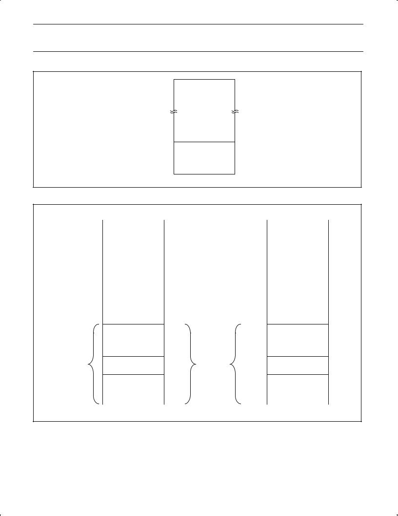
Philips Semiconductors |
Preliminary specification |
XA 16-bit microcontroller
32 K/1 K OTP/ROM/ROMless, 8-channel 8-bit A/D, low voltage (2.7 V±5.5 V), I2C, 2 UARTs, 16 MB address range
XA-S3
FFFFFh
Up to 16 MB
Total Code
Memory
8000h
7FFFh
32 kB On-chip
Code Memory
0000h
SU01219
Figure 1. XA-S3 program memory map
Data Segment 0 |
|
Other Data Segments |
|
|
FFFFh |
FFFFh |
|
|
|
||
Data Memory |
Data Memory |
(Indirectly Addressed, |
(Indirectly Addressed, |
Off-Chip) |
Off-Chip) |
|
|
0400h |
|
0400h |
|
|
|
|
03FFh |
|
03FFh |
|
|
|
Data Memory |
|
|
|
Data Memory |
|
|
(Directly or Indirectly |
|
|
|
(Directly or Indirectly |
|
|
Addressable, On-Chip |
|
Directly |
|
Addressable, On-Chip |
|
1 kB |
|
0040h |
0040h |
|
||
On-Chip Data |
(Bit-Addressable |
003Fh |
Addressed |
003Fh |
(Bit-Addressable |
|
Memory |
|
Data |
|
|||
Data Area) |
|
|
Data Area) |
|||
0020h |
(1 k per |
0020h |
||||
(RAM) |
||||||
|
|
|||||
|
|
001Fh |
Segment) |
001Fh |
|
|
|
Data Memory |
|
|
|
Data Memory |
|
|
(Directly or Indirectly |
|
|
|
(Directly or Indirectly |
|
|
Addressable, On-Chip |
|
|
|
Addressable, Off-Chip |
|
|
|
0000h |
|
0000h |
|
|
|
|
|
|
SU01220
Figure 2. XA-S3 data memory map
2000 Dec 01 |
13 |

Philips Semiconductors |
Preliminary specification |
XA 16-bit microcontroller
32 K/1 K OTP/ROM/ROMless, 8-channel 8-bit A/D, low voltage (2.7 V±5.5 V), I2C, 2 UARTs, 16 MB address range
XA-S3
FUNCTIONAL DESCRIPTION
Details of XA-S3 functions will be described in the following sections.
Analog to Digital converter
The XA-S3 has an 8-channel, 8-bit A/D converter with 8 sets of result registers, single scan and multiple scan operating modes. The A/D also has a 10-bit conversion mode that provides greater result resolution. The A/D input range is limited to 0 to AVDD (3.3 V max.). The A/D inputs are on Port 5. Analog Power and Ground as well as
AVREF+ and AVREF± must be supplied in order for the A/D converter to be used. Prior to enabling the A/D converter or driving analog signals
into the A/D inputs, the port configurations for the pins being used as A/D inputs must be set to the ªoffº (high impedance, input only) mode.
A/D timing can be adapted to the application clock frequency in order to provide the fastest possible conversion.
A/D converter operation is controlled through the ADCON (A/D Control) register, see Figure 1. Bits in ADCON start and stop the A/D, flag conversion completion, and select the converter operating modes. When 10-bit resolution is needed, the A/D mode may be set to give 10 result bits by setting the ADRES bit to 1. In this mode, the A/D takes longer to complete a conversion, and the timing must be set differently in ADCFG.
A/D Conversion Modes
The A/D converter supports a single scan mode and a continuous scan mode. In either mode, one or more A/D channels may be converted. The ADCS register determines which channels are converted. If the corresponding bit in the ADCS register is set, that channel is selected for conversions, otherwise that channel is skipped. The ADCS register is detailed in Figure 2.
For any A/D conversion, the results are stored in ADRSHn, corresponding to the A/D channel just converted. For a 10-bit conversion, the two least significant bits are read from the upper end
of register ADRSL. These bits must be read before another conversion is begun.
A/D conversions are begun by setting the A/D Start and STatus bit in ADCON. In the single scan mode, all of the channels selected by bits in the ADCS register will be converted once. The ADINT flag is set when the last channel is converted. In the continuous scan mode, the A/D converter continuously converts all A/D channels selected by bits in the ADCS register. The ADINT flag is set when all channels have been converted once.
The A/D converter can generate an interrupt when the ADINT flag is set. This will occur if the A/D interrupt is enabled (via the EAD bit in IEL), the interrupt system is enabled (via the EA bit in IEL), and the
A/D interrupt priority (specified in IPA3 bits 3 to 0) is higher than the currently running code (PSW bits IM3 through IM0) and any other pending interrupt. ADINT must be cleared by software.
A/D Timing Configuration
The A/D sampling and conversion timing may be optimized for the particular oscillator frequency and input drive characteristics of the application. Because A/D operation is mostly dependent on real-time effects (charging time of sampling capacitors, settling time of the comparator, etc.), A/D conversion times are not necessarily much longer at slower clock frequencies. The A/D timing is controlled by the ADCFG register, as shown in Figure 3, Table 2 and Table 3.
The primary effect of ADCFG settings is to adjust the A/D sample and hold time to be relatively constant over various clock frequencies. Two settings (value 6 and B) are provided to allow fast conversions with a lower external source driving the A/D inputs.
These settings provide double the sample time at the same frequency. Of course, settings intended for lower frequencies may also be used at higher frequencies in order to increase the A/D sampling time, but this method has the side effect of significantly increasing A/D conversion times.
ADCON |
Address:43Eh |
|
MSB |
|
|
|
|
|
|
|
LSB |
||
|
|
|
|
|
|
|
|
|
|
|
|||
Bit Addressable |
|
|
|
|
|
|
|
|
|
|
|
|
|
|
|
Ð |
|
Ð |
Ð |
Ð |
ADRES |
ADMOD |
ADSST |
ADINT |
|
||
Reset Value: 00h |
|
|
|
|
|||||||||
|
|
|
|
|
|
|
|
|
|
|
|
||
BIT |
|
SYMBOL |
FUNCTION |
|
|
|
|
|
|
|
|||
ADCON.7 |
Ð |
Reserved for future use. Should not be set to 1 by user programs. |
|
|
|||||||||
ADCON.6 |
Ð |
Reserved for future use. Should not be set to 1 by user programs. |
|
|
|||||||||
ADCON.5 |
Ð |
Reserved for future use. Should not be set to 1 by user programs. |
|
|
|||||||||
ADCON.4 |
Ð |
Reserved for future use. Should not be set to 1 by user programs. |
|
|
|||||||||
ADCON.3 |
ADRES |
Selects 8-bit (0) or 10-bit (1) conversion mode. |
|
|
|||||||||
ADCON.2 |
ADMOD |
A/D mode select. |
|
|
|
|
|
|
|
||||
|
|
|
|
1 = continuous scan of selected inputs after a start of the A/D. |
|
|
|||||||
|
|
|
|
0 = single scan of selected inputs after a start of the A/D. |
|
|
|||||||
ADCON.1 |
ADSST |
A/D start and status. Setting this bit by software starts the A/D conversion of the selected A/D |
|||||||||||
|
|
|
inputs. ADSST remains set as long as the A/D is in operation. In continuous conversion mode, |
||||||||||
|
|
|
ADSST will remain set unless the A/D is stopped by software. While ADSST is set, new start |
||||||||||
|
|
|
commands are ignored. An A/D conversion is progress may be aborted by software clearing |
||||||||||
|
|
|
ADSST. |
|
|
|
|
|
|
|
|
|
|
ADCON.0 |
ADINT |
A/D conversion complete/interrupt flag. This flag is set when all selected A/D channels are |
|||||||||||
|
|
|
converted in either the single scan or continuous scan modes. Must be cleared by software. |
||||||||||
|
|
|
|
|
|
|
|
|
|
|
|
|
SU01229 |
|
|
|
|
|
|
|
|
|
|
|
|
|
|
|
|
|
|
|
Figure 1. A/D Control Register (ADCON) |
|
|
||||||
2000 Dec 01 |
14 |

Philips Semiconductors |
Preliminary specification |
XA 16-bit microcontroller
32 K/1 K OTP/ROM/ROMless, 8-channel 8-bit A/D, low voltage (2.7 V±5.5 V), I2C, 2 UARTs, 16 MB address range
XA-S3
ADCS |
Address:43Fh |
|
MSB |
|
|
|
|
|
|
|
|
|
LSB |
|
||||
|
|
|
|
|
|
|
|
|
|
|
|
|
|
|
||||
Bit Addressable |
|
|
|
|
|
|
|
|
|
|
|
|
|
|
|
|
|
|
|
|
|
ADCS7 |
ADCS6 |
ADCS5 |
ADCS4 |
|
ADCS3 |
ADCS2 |
ADCS1 |
ADCS0 |
|
|
|||||
Reset Value: 00h |
|
|
|
|
|
|
||||||||||||
|
|
|
|
|
|
|
|
|
|
|
|
|
|
|
|
|
||
BIT |
SYMBOL |
FUNCTION |
|
|
|
|
|
|
|
|
|
|
|
|||||
ADCS.7 |
ADCS7 |
A/D channel 7 select bit. |
|
|
|
|
|
|
|
|
|
|
||||||
ADCS.6 |
ADCS6 |
A/D channel 6 select bit. |
|
|
|
|
|
|
|
|
|
|
||||||
ADCS.5 |
ADCS5 |
A/D channel 5 select bit. |
|
|
|
|
|
|
|
|
|
|
||||||
ADCS.4 |
ADCS4 |
A/D channel 4 select bit. |
|
|
|
|
|
|
|
|
|
|
||||||
ADCS.3 |
ADCS3 |
A/D channel 3 select bit. |
|
|
|
|
|
|
|
|
|
|
||||||
ADCS.2 |
ADCS2 |
A/D channel 2 select bit. |
|
|
|
|
|
|
|
|
|
|
||||||
ADCS.1 |
ADCS1 |
A/D channel 1 select bit. |
|
|
|
|
|
|
|
|
|
|
||||||
ADCS.0 |
ADCS0 |
A/D channel 0 select bit. |
|
|
|
|
|
SU00939 |
|
|||||||||
|
|
|
|
|
|
|
|
|
|
|
|
|
|
|
||||
|
|
|
|
|
|
|
|
|
|
|
|
|
|
|
|
|
|
|
|
|
|
|
|
Figure 2. A/D Channel Select Register (ADCS) |
|
|
|
|
|
||||||||
|
|
|
|
|
|
|
|
|
|
|
|
|
|
|
|
|
|
|
ADCFG |
Address:4B9h |
|
MSB |
|
|
|
|
|
|
|
|
|
LSB |
|
||||
|
|
|
|
|
|
|
|
|
|
|
|
|
|
|
||||
Not bit Addressable |
|
|
|
|
|
|
|
|
|
|
|
|
|
|
|
|
|
|
|
|
|
|
|
|
|
|
|
|
|
|
|
|
|
|
|
||
Reset Value: 00h |
|
|
|
Ð |
Ð |
Ð |
Ð |
|
A/D Timing Configuration |
|
|
|
||||||
|
|
|
|
|
|
|
|
|
|
|
|
|
|
|
|
|
|
|
BIT |
SYMBOL |
FUNCTION |
|
|
|
|
|
|
|
|
|
|
|
|||||
ADCFG.7 |
Ð |
Reserved for future use. Should not be set to 1 by user programs. |
|
|
|
|
|
|||||||||||
ADCFG.6 |
Ð |
Reserved for future use. Should not be set to 1 by user programs. |
|
|
|
|
|
|||||||||||
ADCFG.5 |
Ð |
Reserved for future use. Should not be set to 1 by user programs. |
|
|
|
|
|
|||||||||||
ADCFG.4 |
Ð |
Reserved for future use. Should not be set to 1 by user programs. |
|
|
|
|
|
|||||||||||
ADCFG.3±0 |
ADCFG |
A/D timing configuration (see text and table). |
|
|
|
|
|
|||||||||||
|
|
|
|
|
|
|
|
|
|
|
|
|
|
SU00940 |
|
|||
|
|
|
|
|
|
|
|
|
|
|
|
|
||||||
|
|
|
|
|
Figure 3. A/D Timing Configuration Register (ADCFG) |
|
|
|
|
|
||||||||
Table 2. A/D Timing Configuration |
|
|
|
|
|
|
|
|
|
|
|
|
|
|||||
|
|
|
|
|
|
|
|
|
|
|
|
|
|
|
|
|||
ADCFG.3±0 |
|
Max. Oscillator |
|
|
|
Conversion Time |
|
|
|
Sampling Time |
|
|||||||
|
|
|
|
|
|
|
|
|
|
|
|
|
||||||
|
Frequency (MHz) |
|
|
Osc. Clocks |
|
μsec at max. Osc. |
|
|
|
(Osc. Clocks) |
|
|||||||
|
|
|
|
|
|
|
|
|
|
|||||||||
|
|
|
|
|
|
|
|
|
|
|
|
|
|
|||||
|
|
|
|
|
|
|
|
|
|
|
|
|
|
|||||
0h (0000) |
|
|
|
6.66 |
|
|
72 |
|
|
10.81 |
|
4 |
|
|||||
|
|
|
|
|
|
|
|
|
|
|
|
|
|
|
||||
1h (0001) |
|
|
|
10 |
|
|
76 |
|
|
7.6 |
|
|
6 |
|
||||
|
|
|
|
|
|
|
|
|
|
|
|
|
|
|
||||
2h (0010) |
|
|
|
11.11 |
|
|
80 |
|
|
7.2 |
|
|
8 |
|
||||
|
|
|
|
|
|
|
|
|
|
|
|
|
|
|
||||
3h (0011) |
|
|
|
13.33 |
|
|
96 |
|
|
7.2 |
|
|
8 |
|
||||
|
|
|
|
|
|
|
|
|
|
|
|
|
|
|
||||
4h (0100) |
|
|
|
16.66 |
|
|
100 |
|
|
6.0 |
|
|
10 |
|
||||
|
|
|
|
|
|
|
|
|
|
|
|
|
|
|
||||
5h (0101) |
|
|
|
20 |
|
|
104 |
|
|
5.2 |
|
|
12 |
|
||||
|
|
|
|
|
|
|
|
|
|
|
|
|
|
|
||||
6h (0110)1 |
|
|
|
20 |
|
|
116 |
|
|
5.8 |
|
|
24 |
|
||||
7h (0111) |
|
|
|
22.2 |
|
|
108 |
|
|
4.86 |
|
|
14 |
|
||||
|
|
|
|
|
|
|
|
|
|
|
|
|
|
|
||||
8h (1000) |
|
|
|
23.3 |
|
|
124 |
|
|
5.32 |
|
|
14 |
|
||||
|
|
|
|
|
|
|
|
|
|
|
|
|
|
|
||||
9h (1001) |
|
|
|
26.6 |
|
|
128 |
|
|
4.81 |
|
|
16 |
|
||||
|
|
|
|
|
|
|
|
|
|
|
|
|
|
|
||||
Ah (1010) |
|
|
|
30 |
|
|
132 |
|
|
4.4 |
|
|
18 |
|
||||
|
|
|
|
|
|
|
|
|
|
|
|
|
|
|
||||
Bh (1011)1 |
|
|
|
30 |
|
|
146 |
|
|
4.87 |
|
|
32 |
|
||||
Ch (1100) |
|
|
|
± |
|
|
|
136 |
|
|
4.25 |
|
|
20 |
|
|||
|
|
|
|
|
|
|
|
|
|
|
|
|
|
|
|
|||
Dh (1101) |
|
|
|
± |
|
|
|
152 |
|
|
4.56 |
|
|
20 |
|
|||
|
|
|
|
|
|
|
|
|
|
|
|
|
|
|
|
|||
Eh (1110) |
|
|
|
± |
|
|
|
172 |
|
|
4.7 |
|
|
22 |
|
|||
|
|
|
|
|
|
|
|
|
|
|
|
|
|
|
|
|||
Fh (1111) |
|
|
|
± |
|
|
|
176 |
|
|
4.4 |
|
|
24 |
|
|||
|
|
|
|
|
|
|
|
|
|
|
|
|
|
|
|
|
|
|
NOTE:
1. These settings provide additional A/D input sampling time, in order to allow accurate readings with a higher external source impedance.
2000 Dec 01 |
15 |
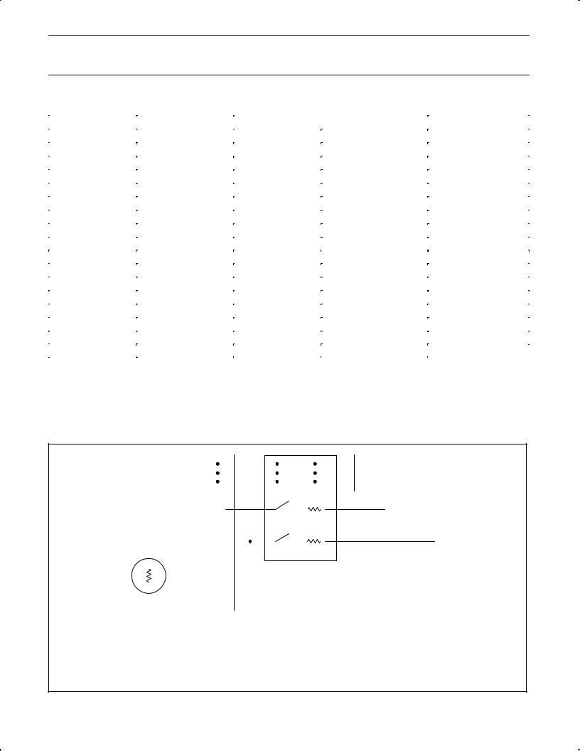
Philips Semiconductors |
Preliminary specification |
XA 16-bit microcontroller
32 K/1 K OTP/ROM/ROMless, 8-channel 8-bit A/D, low voltage (2.7 V±5.5 V), I2C, 2 UARTs, 16 MB address range
Table 3. A/D Timing Configuration for 10-bit Mode
XA-S3
|
ADCFG.3±0 |
Max. Oscillator |
|
Conversion Time |
Sampling Time |
|
|
|
|
|
|||
|
Frequency (MHz) |
Osc. Clocks |
|
μsec at max. Osc. |
(Osc. Clocks) |
|
|
|
|
||||
|
|
|
|
|
||
|
|
|
|
|
|
|
0h |
(0000) |
6.66 |
88 |
|
13.21 |
4 |
|
|
|
|
|
|
|
1h |
(0001) |
8 |
92 |
|
9.2 |
6 |
|
|
|
|
|
|
|
2h |
(0010) |
8 |
96 |
|
8.64 |
8 |
|
|
|
|
|
|
|
3h |
(0011) |
12 |
116 |
|
8.7 |
8 |
|
|
|
|
|
|
|
4h |
(0100) |
12 |
120 |
|
7.2 |
10 |
|
|
|
|
|
|
|
5h |
(0101) |
12 |
124 |
|
6.2 |
12 |
|
|
|
|
|
|
|
6h |
(0110) |
12 |
136 |
|
6.8 |
24 |
|
|
|
|
|
|
|
7h |
(0111) |
12 |
128 |
|
5.77 |
14 |
|
|
|
|
|
|
|
8h |
(1000) |
13 |
148 |
|
6.35 |
14 |
|
|
|
|
|
|
|
9h |
(1001) |
13 |
152 |
|
5.71 |
16 |
|
|
|
|
|
|
|
Ah (1010) |
13 |
156 |
|
5.2 |
18 |
|
|
|
|
|
|
|
|
Bh (1011) |
13 |
170 |
|
5.67 |
32 |
|
|
|
|
|
|
|
|
Ch (1100) |
13 |
160 |
|
5.0 |
20 |
|
|
|
|
|
|
|
|
Dh (1101) |
16 |
180 |
|
5.41 |
20 |
|
|
|
|
|
|
|
|
Eh (1110) |
20 |
204 |
|
5.57 |
22 |
|
|
|
|
|
|
|
|
Fh (1111) |
20 |
208 |
|
5.2 |
24 |
|
|
|
|
|
|
|
|
A/D Inputs
In order to obtain accurate measurements with the A/D Converter, the source drive must be sufficient to adequately charge the sampling capacitor during the sampling time. Figure 4 shows the equivalent resistance and capacitance related to the A/D inputs.
A/D timing configurations indicated in Table 1 allow for full A/D
accuracy (according to the A/D specifications) assuming a source resistance of less than or equal to 20kΩ. Larger source resistances may be accommodated by increasing the sampling time with a different A/D timing configuration.
|
|
|
|
|
|
|
|
SmN+1 |
RmN+1 |
|
|||||
|
|
|
|
|
|
|
ADN+1 |
|
|
|
|
|
|||
|
|
|
|
|
|
|
|
SmN |
RmN |
TO COMPARATOR |
|||||
|
|
|
|
|
|
|
ADN |
|
|
|
|
||||
|
|
|
|
|
|
|
|
|
|
|
|
||||
|
|
|
+ |
|
|
|
|
|
|
|
|
|
|
||
|
|
|
|
|
|
|
|
|
Multiplexer |
|
|||||
|
|
|
|
|
|
|
|
||||||||
RS |
|
|
|||||||||||||
|
|
|
|
|
|
|
|
|
|
||||||
|
|
|
|
|
|
|
|
CS |
|
|
|
|
CC |
||
|
|
|
|
|
|
|
VANALOG |
|
|
|
|
||||
|
|
|
|
|
|
|
|
|
|
|
|
|
|
|
|
|
|
|
|
|
|
|
INPUT |
|
|
|
|
|
|
|
|
Rm (multiplexer resistance) |
= |
3 kΩ maximum |
|
|
|
|
|
||||||||
CS (pin capacitance) |
= |
10 pF maximum |
|
|
|
|
|
||||||||
CC (sampling capacitor) |
= |
2 pF maximum |
|
|
|
|
|
||||||||
RS (source resistance) |
= Recommended less than 20kΩ for full specified accuracy. This allows time for the sampling |
||||||||||||||
capacitor (CC) to fully charge while the multiplexer switch is closed. Please note that sampling causes the analog input to present a varying load to the pin.
SU00948
Figure 4. A/D Input: Equivalent Circuit
2000 Dec 01 |
16 |
Loading...