


MN13822
Panasonic MN13822, MN13812, MN1382, MN1381, MN1380 Datasheet
...
1
Microcomputer Peripheral LSIs
MN1380 Series
CMOS LSIs for Voltage Detection
Overview
The MN1380 series are elements that monitor the power
supply voltage supplied to microcomputers and other LSI
systems and issue reset signals for initializing the system
after the power is first applied or for preventing runaway
operation when the supply voltage fluctuates.
There is a choice of three output types: CMOS output,
N-channel open drain output, and inverted CMOS out-
put. There are also three package types: M, TO-92, and a
mini type for surface mounting.
Choose the ideal element for your application from the
series' wide selection of detection ranks (17 ranks between
2.0 and 4.9 volts), output types, and package types.
Features
Three-pin element requiring no adjustment
Wide selection of detection ranks (17 ranks between
2.0 and 4.9 volts)
Highly precise detection voltage
Detection voltage with hysteresis characteristic
∆VD = 50 mV for ranks C to K
∆VD = 100 mV for ranks L to U
Low current consumption: I
DD
= 1µA (typ.) for V
DD
= 5 V
Low fluctuation in detection voltage with tempera-
ture (typ. 1 mV/˚C)
Wide selection of output types: CMOS output, N-
channel open drain output, and inverted CMOS
output
Wide selection of package types: M, TO-92, and a
mini type for surface mounting.
Applications
Battery checkers
Power outage detectors
Level discriminators
Memory backup systems
Microcomputer reset circuits
Reset circuits for other electronic circuits
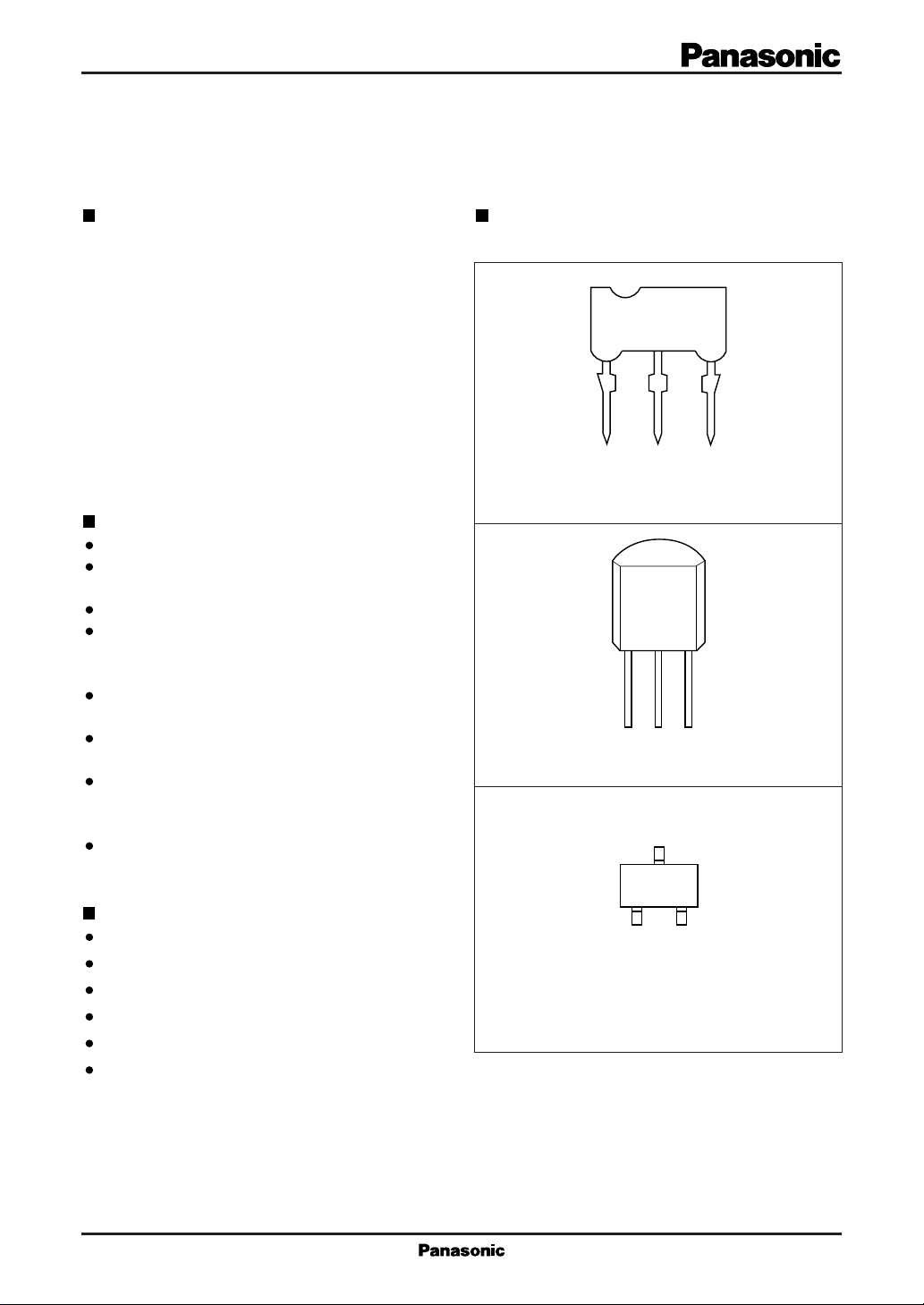
Pin Assignment
M type package
3
21
23
MN1380 - R
1381
23R
12
3
1
2
3
LCR
TO-92 type package
Mini type package
1=OUT
2=V
DD
3=V
SS
2
MN1380 Series Microcomputer Peripheral LSIs
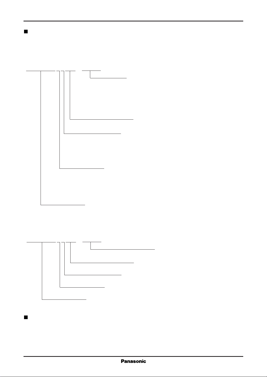
MN1380 Series Naming Conventions
The MN1380 series offers a wide selection of detection ranks, output types, package types, and packaging. All
combinations use the following naming conventions. When ordering, be sure to give the correct part number using
these naming conventions.
Winding direction for tape packaging
(TA) ...... Tape packaging for TO-92 type package
(TX)...... Embossed tape packing for mini type package
(TW)..... Embossed tape packing for mini type package
For further details, see the package specifications.
Detection voltage rank (C to U)
Output type:
Blank ········ CMOS output
1················ N-channel open drain output
2 ················ inverted CMOS output
Package:
0 ················ M type package
1 ················ TO-92 type package
2 ················ Mini type package
Matsushita Electronics Corporation MN1380 series of voltage detection CMOS
LSIs with low current consumptions
MN13821–R (TW)
(Example)
Embossed tape packaging
R rank (detection voltage of 4.0 to 4.3 V)
N-channel open drain output
Mini type package
MN1380 series of voltage detection CMOS LSIs with low current consumption
MN13801–R (TA)
Minimum Packaging Unit
Bulk (M and TO-92 types) ·············· 1,000
Magazine (Mini type) ······················ 50
Taping (Mini and TO-92 types)·······3,000
3
Microcomputer Peripheral LSIs MN1380 Series
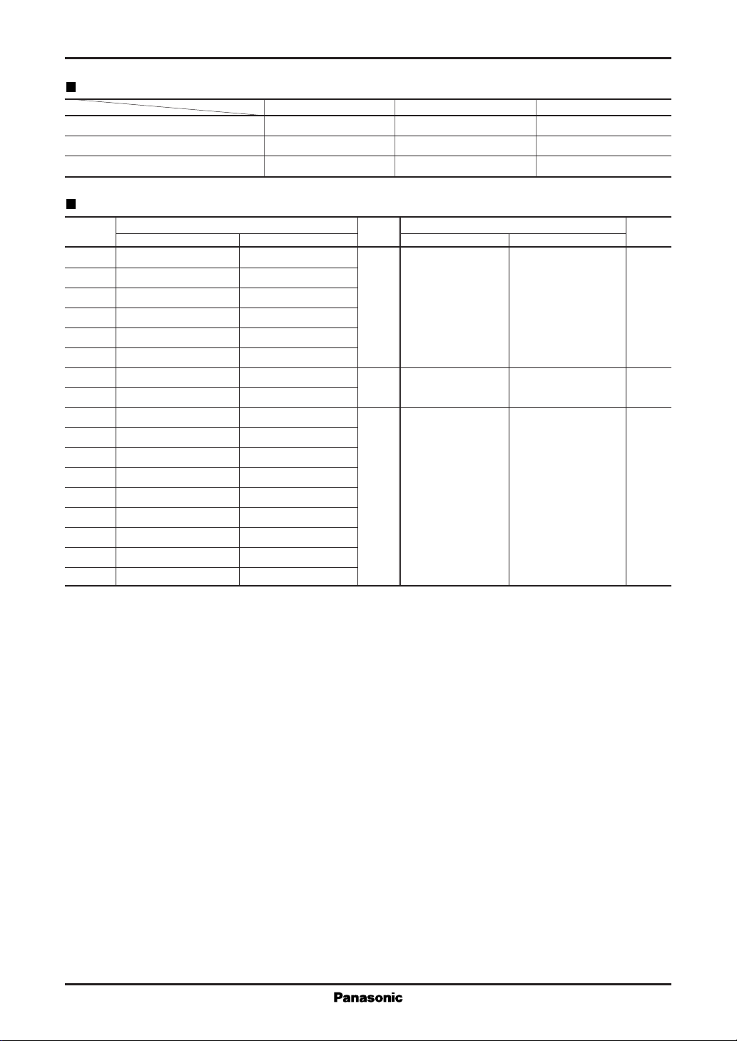
Series Lineup
Output
Package
M type Package TO-92 type Package Mini type Package
CMOS output MN1380 MN1381 MN1382
N-channel open drain output MN13801 MN13811 MN13821
Inverted CMOS output MN13802 MN13812 MN13822
Detection Ranks (on Voltage)
Rank
Detection Voltage for Drop in Power Supply Voltage (V
DL
)
Unit
Detection Voltage Hysteresis Width (∆VD)
Unit
min max min max
C 2.0 2.2
D 2.1 2.3
E 2.2 2.4
V 50 300 mV
F 2.3 2.5
G 2.4 2.6
H 2.5 2.7
J 2.6 2.9
V 50 300 mV
K 2.8 3.1
L 3.0 3.3
M 3.2 3.5
N 3.4 3.7
P 3.6 3.9
Q 3.8 4.1 V 100 300 mV
R 4.0 4.3
S 4.2 4.5
T 4.4 4.7
U 4.6 4.9

4
MN1380 Series Microcomputer Peripheral LSIs
Block Diagram
Pin Descriptions
Pin No. Symbol Function Description
1 OUT Reset signal output pin
2V
DD
Power supply pin
3V
SS
Ground pin
Note *
1
: Circuits vary slightly depending on the output type (CMOS output, N-channel open drain output, or inverted CMOS
output)
Voltage
Reference 1
Voltage
Reference 2
Level Converter
Comparator
Comparator
Output Circuit
*
1
V
DD
OUT
V
SS
2
1
3
+
–
+
–
5
Microcomputer Peripheral LSIs MN1380 Series
Electrical Characteristics
1) DC Characteristics V
SS
=0V, Ta=–20˚C to +70˚C
Parameter Symbol Conditions min typ max Unit
Power supply current I
DD
V
DD
= 5 V
*1
15µA
Load resistance = 10 kW
Detection voltage for drop
V
DL
Ta=25˚C
*
2
*
2
V
in power supply voltage
*2
See Figures 1 and 4.
Detection voltage hysteresis
∆VD
*
2
*
2
mV
width
*2
"H" level output voltage V
OH
CMOS output I
OH
=– 40µA 0.8V
DD
V
DD
Inverted V
DD
=1.8V
0.8
V
DD
V
CMOS output I
OH
=– 0.5mA –1.5
"L" level output voltage V
OL
N-channel open V
DD
=1.8V V
SS
0.4
drain output I
OL
=0.7mA
V
Inverted V
DD
=6.0V V
SS
0.6
CMOS output I
OH
=0.3mA
Absolute Maximum Ratings V
SS
=0V, Ta=25˚C
Parameter Symbol Rating Unit
Power supply voltage V
DD
7.0 V
Output voltage V
O
– 0.3 to V
DD
+0.3 V
Operating ambient temperature Ta –20 to +70 ˚C
Storage temperature T
stg
–55 to +125 ˚C
Recommended Operating Conditions
V
SS
=0V, Ta=25˚C
Parameter Symbol Conditions min typ max Unit
Power supply
V
DD
See Figures 1 and 4. 1.5 6.0 V
voltage
Notes
*
1
: This includes the output pin's leakage current.
*
2
: For particulars, see the detection voltage rank table.
6
MN1380 Series Microcomputer Peripheral LSIs
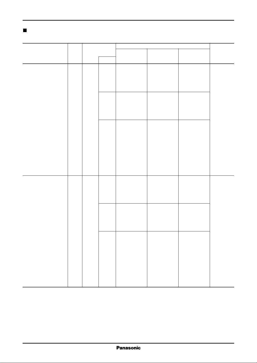
2) AC Characteristics V
SS
=0V, Ta=25˚C
Parameter Symbol Conditions
Allowable Value (typ)
Unit
MN1380 MN13801 MN13802
MN1381 MN13811 MN13812
Rank MN1382 MN13821 MN13822
C
D
E 3.0 2.5 230.0
F
G
See H
Reset release time t
OH
Figures J 3.0 3.0 100.0 µs
2 and 3. K
L
M
N
P
Q 2.0 4.0 30.0
R
S
T
C
D
E 250.0 160.0 3.0
F
G
See H
Reset time t
OL
Figures J 115.0 100.0 3.0 µs
2 and 3. K
L
M
N
P
Q 15.0 35.0 3.0
R
S
T
Electrical Characteristics (continued)
 Loading...