


 Loading...
PAMS Technical Documentation
NSE–8/9 Series Transceivers
Chapter 2
System Module
Amendment 05/00

NSE–8/9 |
PAMS |
System Module |
Technical Documentation |
|
Contents
|
Page No |
Technical Information . . . . . . . . . . . . . . . . . . . . . . . . . . . . . . . . . . . . . . . . . . . |
. . 2– 5 |
Operating Modes . . . . . . . . . . . . . . . . . . . . . . . . . . . . . . . . . . . . . . . . . . . . |
. . 2– 6 |
Maximum ratings . . . . . . . . . . . . . . . . . . . . . . . . . . . . . . . . . . . . . . . . . . . . |
. . 2– 7 |
DC Characteristics . . . . . . . . . . . . . . . . . . . . . . . . . . . . . . . . . . . . . . . . . . |
. . 2– 7 |
External Signals and Connections . . . . . . . . . . . . . . . . . . . . . . . . . . . . . |
. . 2– 10 |
Internal Signals and Connections . . . . . . . . . . . . . . . . . . . . . . . . . . . . . . |
. . 2– 21 |
Technical Summary . . . . . . . . . . . . . . . . . . . . . . . . . . . . . . . . . . . . . . . . . . |
. . 2– 31 |
Baseband . . . . . . . . . . . . . . . . . . . . . . . . . . . . . . . . . . . . . . . . . . . . . . . . . . . . . |
. . 2– 34 |
Functional Description . . . . . . . . . . . . . . . . . . . . . . . . . . . . . . . . . . . . . . . |
. . 2– 34 |
Charger Initiated Power Up Procedure . . . . . . . . . . . . . . . . . . . . . . |
. . 2– 34 |
Power Button Initiated Power Up Procedure . . . . . . . . . . . . . . . . . |
. . 2– 35 |
Real Time Clock Initiated Power Up Procedure . . . . . . . . . . . . . . . |
. . 2– 36 |
Power Down Schemes . . . . . . . . . . . . . . . . . . . . . . . . . . . . . . . . . . . . . . . |
. . 2– 37 |
Clocking Concept . . . . . . . . . . . . . . . . . . . . . . . . . . . . . . . . . . . . . . . . |
. . 2– 40 |
Resets and Watchdogs . . . . . . . . . . . . . . . . . . . . . . . . . . . . . . . . . . . . . . |
. . 2– 41 |
Power Supply . . . . . . . . . . . . . . . . . . . . . . . . . . . . . . . . . . . . . . . . . . . . . . . |
. . 2– 42 |
Baseband supplies, CCONT . . . . . . . . . . . . . . . . . . . . . . . . . . . . . . . |
. . 2– 45 |
Charging . . . . . . . . . . . . . . . . . . . . . . . . . . . . . . . . . . . . . . . . . . . . . . . . |
. . 2– 47 |
Baseband ADC’s . . . . . . . . . . . . . . . . . . . . . . . . . . . . . . . . . . . . . . . . . |
. . 2– 50 |
Digital Part . . . . . . . . . . . . . . . . . . . . . . . . . . . . . . . . . . . . . . . . . . . . . . . . . |
. . 2– 53 |
MAD2PR1 system ASIC . . . . . . . . . . . . . . . . . . . . . . . . . . . . . . . . . . |
. . 2– 53 |
SRAM Memory . . . . . . . . . . . . . . . . . . . . . . . . . . . . . . . . . . . . . . . . . . |
. . 2– 58 |
EEPROM Memory . . . . . . . . . . . . . . . . . . . . . . . . . . . . . . . . . . . . . . . . |
. . 2– 59 |
FLASH Memory . . . . . . . . . . . . . . . . . . . . . . . . . . . . . . . . . . . . . . . . . . |
. . 2– 59 |
Audio . . . . . . . . . . . . . . . . . . . . . . . . . . . . . . . . . . . . . . . . . . . . . . . . . . . . . . |
. . 2– 62 |
UI . . . . . . . . . . . . . . . . . . . . . . . . . . . . . . . . . . . . . . . . . . . . . . . . . . . . . . . . . . . . |
. . 2– 68 |
Backlight . . . . . . . . . . . . . . . . . . . . . . . . . . . . . . . . . . . . . . . . . . . . . . . . . . . |
. . 2– 69 |
Buzzer . . . . . . . . . . . . . . . . . . . . . . . . . . . . . . . . . . . . . . . . . . . . . . . . . . . . . |
. . 2– 69 |
Vibra, NSE–9 only . . . . . . . . . . . . . . . . . . . . . . . . . . . . . . . . . . . . . . . . . . . |
. . 2– 70 |
LCD . . . . . . . . . . . . . . . . . . . . . . . . . . . . . . . . . . . . . . . . . . . . . . . . . . . . . . . |
. . 2– 70 |
Keyboard . . . . . . . . . . . . . . . . . . . . . . . . . . . . . . . . . . . . . . . . . . . . . . . . . . |
. . 2– 71 |
Page 2– 2 |
Amendment 05/00 |

PAMS |
NSE–8/9 |
|
|
Technical Documentation |
System Module |
|
RF . . . . . . . . . . . . . . . . . . . . . . . . . . . . . . . . . . . . . . . . . . . . . . . . . . . . . . . . . . . . . 2– 72
DC Regulators . . . . . . . . . . . . . . . . . . . . . . . . . . . . . . . . . . . . . . . . . . . . . . . . 2– 74
Frequency Synthesizers . . . . . . . . . . . . . . . . . . . . . . . . . . . . . . . . . . . . . . . . 2– 75
Receiver . . . . . . . . . . . . . . . . . . . . . . . . . . . . . . . . . . . . . . . . . . . . . . . . . . . . . 2– 76 GSM900 Front–End . . . . . . . . . . . . . . . . . . . . . . . . . . . . . . . . . . . . . . . . 2– 77 GSM1800 Front–End . . . . . . . . . . . . . . . . . . . . . . . . . . . . . . . . . . . . . . . 2– 78 Common Receiver parts for GSM900 and GSM1800 . . . . . . . . . . . . 2– 78 Transmitter . . . . . . . . . . . . . . . . . . . . . . . . . . . . . . . . . . . . . . . . . . . . . . . . . . . 2– 80
Common Transmitter Part . . . . . . . . . . . . . . . . . . . . . . . . . . . . . . . . . . . 2– 81 GSM900 Transmitter . . . . . . . . . . . . . . . . . . . . . . . . . . . . . . . . . . . . . . . 2– 81 GSM1800 Transmitter . . . . . . . . . . . . . . . . . . . . . . . . . . . . . . . . . . . . . . 2– 82 Transmitter Power Control for GSM900 and GSM1800 . . . . . . . . . . 2– 83
AGC . . . . . . . . . . . . . . . . . . . . . . . . . . . . . . . . . . . . . . . . . . . . . . . . . . . . . . . . . 2– 84 AFC function . . . . . . . . . . . . . . . . . . . . . . . . . . . . . . . . . . . . . . . . . . . . . . . . . 2– 84 Interfacing . . . . . . . . . . . . . . . . . . . . . . . . . . . . . . . . . . . . . . . . . . . . . . . . . . . . 2– 85 RX: . . . . . . . . . . . . . . . . . . . . . . . . . . . . . . . . . . . . . . . . . . . . . . . . . . . . . . . 2– 85
TX: . . . . . . . . . . . . . . . . . . . . . . . . . . . . . . . . . . . . . . . . . . . . . . . . . . . . . . . 2– 86
Parts Lists . . . . . . . . . . . . . . . . . . . . . . . . . . . . . . . . . . . . . . . . . . . . . . . . . . . . . . . .
System Module GF7_17 . . . . . . . . . . . . . . . . . . . . . . . . . . . . . . . . . . . . . . . 2– 89
System Module GF7_18 . . . . . . . . . . . . . . . . . . . . . . . . . . . . . . . . . . . . . . . 2– 102
System Module GF7_20B . . . . . . . . . . . . . . . . . . . . . . . . . . . . . . . . . . . . . . 2– 115
System Module GD7_18 . . . . . . . . . . . . . . . . . . . . . . . . . . . . . . . . . . . . . . . 2– 128
System Module GD7_21 . . . . . . . . . . . . . . . . . . . . . . . . . . . . . . . . . . . . . . . 2– 141
Hardware ID Chart . . . . . . . . . . . . . . . . . . . . . . . . . . . . . . . . . . . . . . . . . . . . . . . 2– 154
Amendment 05/00 |
Page 2– 3 |

NSE–8/9 |
PAMS |
System Module |
Technical Documentation |
|
Table of Figures
Figure 1. |
SIM connector, X100 and Battery terminals, . . . . . . . . . . . . . . |
2– 10 |
Figure 2. Display Connector pin location . . . . . . . . . . . . . . . . . . . . . . . . . . |
2– 12 |
|
Figure 3. Bottom Connector, X503, pin locations (top View) . . . . . . . . . . |
2– 15 |
|
Figure 4. Bottom Connector, X503, pin locations (BottomView) . . . . . . . |
2– 15 |
|
Figure 5. Internal Speaker Pads . . . . . . . . . . . . . . . . . . . . . . . . . . . . . . . . . . |
2– 19 |
|
Figure 6. Vibra Motor–connetion pads . . . . . . . . . . . . . . . . . . . . . . . . . . . . . |
2– 20 |
|
Figure 7. Baseband Block Diagram . . . . . . . . . . . . . . . . . . . . . . . . . . . . . . . |
2– 31 |
|
Figure 8. |
Clocking Scheme . . . . . . . . . . . . . . . . . . . . . . . . . . . . . . . . . . . . . . |
2– 40 |
Figure 9. |
Reset Scheme . . . . . . . . . . . . . . . . . . . . . . . . . . . . . . . . . . . . . . . . |
2– 41 |
Figure 10. Baseband power Distribution . . . . . . . . . . . . . . . . . . . . . . . . . . . |
2– 43 |
|
Figure 11. |
DC/DC Converter . . . . . . . . . . . . . . . . . . . . . . . . . . . . . . . . . . . . . |
2– 44 |
Figure 12. Principle of SMR power Functions . . . . . . . . . . . . . . . . . . . . . . |
2– 46 |
|
Figure 13. Charging Block Diagram . . . . . . . . . . . . . . . . . . . . . . . . . . . . . . . |
2– 47 |
|
Figure 14. Flash Programming Sequence . . . . . . . . . . . . . . . . . . . . . . . . . |
2– 56 |
|
Figure 15. Sim Card DetX detection levels . . . . . . . . . . . . . . . . . . . . . . . . . |
2– 57 |
|
Figure 16. |
Memory Setup . . . . . . . . . . . . . . . . . . . . . . . . . . . . . . . . . . . . . . . |
2– 58 |
Figure 17. Digital Interface – CCONT and MAD2PR1 . . . . . . . . . . . . . . . |
2– 60 |
|
Figure 18. Digital Interface – COBBA_GJP and MAD2PR1 . . . . . . . . . . |
2– 61 |
|
Figure 19. UI Switch & Transducers . . . . . . . . . . . . . . . . . . . . . . . . . . . . . . |
2– 68 |
|
Figure 20. RF Frequency Plan . . . . . . . . . . . . . . . . . . . . . . . . . . . . . . . . . . . |
2– 73 |
|
Figure 21. Power Distribution Diagram . . . . . . . . . . . . . . . . . . . . . . . . . . . . |
2– 74 |
|
Figure 22. Frequency Synthesiser– Block Diagram . . . . . . . . . . . . . . . . . |
2– 75 |
|
Figure 23. Receiver Block Diagram . . . . . . . . . . . . . . . . . . . . . . . . . . . . . . . |
2– 77 |
|
Figure 24. Transmitter Block Diagram . . . . . . . . . . . . . . . . . . . . . . . . . . . . . |
2– 80 |
|
Figure 25. |
Receiver Interface . . . . . . . . . . . . . . . . . . . . . . . . . . . . . . . . . . . . |
2– 85 |
Figure 26. |
Transmitter Interface . . . . . . . . . . . . . . . . . . . . . . . . . . . . . . . . . |
2– 86 |
Schematics/Layouts |
|
|
(GF7_17) |
. . . . . . . . . . . . . . . . . . . . . . . . . . . . . . . . . . . . . . . . . . . . . . . . . . . . . . . |
A– 1 |
(GF7_18) . |
. . . . . . . . . . . . . . . . . . . . . . . . . . . . . . . . . . . . . . . . . . . . . . . . . . . . . . |
A– 12 |
(GF7_20B) |
. . . . . . . . . . . . . . . . . . . . . . . . . . . . . . . . . . . . . . . . . . . . . . . . . . . . . . |
A– 23 |
(GD7_18) . |
. . . . . . . . . . . . . . . . . . . . . . . . . . . . . . . . . . . . . . . . . . . . . . . . . . . . . . |
A– 34 |
(GD7_21) . |
. . . . . . . . . . . . . . . . . . . . . . . . . . . . . . . . . . . . . . . . . . . . . . . . . . . . . . |
A– 45 |
Page 2– 4 |
Amendment 05/00 |

PAMS |
NSE±8/9 |
|
|
Technical Documentation |
System Module |
|
Technical Information
HD947 is a DCT3.5 based product, i.e. a dual band GSM 900 &
DCS1800, single board concept using the serial version of the MAD2PR1± and COBBA_GJP chip set. HD947 is based on HD945 (PICA) HW with significant modifications in the Baseband as listed below:
±HD947 uses a two cell semi fixed NiMH battery±pack only, giving 2.4V nominal supply voltage. Thus the usual NMP battery interface is modified.
±A special charge control ASIC, PSCC, is used for two cell NiMH charging instead of CHAPS (basically a Chaps modified for 2cells with reduced features).
±The supply voltage inside the phone is delivered by a DC/DC converter, which step up the battery voltage to 3.1 ± 4.2 V supplying the regulators and PA's of the phone.
±The DC/DC converter is supplying 4 different voltages ref. depending upon the required power level and phone state.
±HD947 has a special non DCT3 compatible Bottom connector, which supports no DATA, only chargers and external audio.
±Headset HDC±5 and Handsfree unit PPH±1 are supported.
±The external Audio is dual ended uplink and downlink.
±HD947 supports only internal vibra, and in NSE±9 only.
±No support of FLASH ROM writing outside production or aftersales environment.
±HD947 has a separate serial EEPROM.
±Battery removal detection is changed compared to previous NMP standard.
±An integrated switch IC, UISwitch, is used for buzzer, vibra and backlight driving.
±There are no backup supply for the RTC. The watch may have to be reset after battery removal.
The only difference in the Baseband between GF7 and GD7 is that ºCol 4º pin on the MAD2PR1 is logically HIGH in GF7 and logically LOW in GD7, to indicate to the SW which kind of PCB is in use. The two different versions are made to accommodate the use of two different sets of PA's.
The only Baseband difference between NSE±8 and ±9 is that the vibra is mounted in the mechanical assembly in NSE±9.
Issue 1 07/99 |
Page 2± 5 |

NSE±8/9 |
PAMS |
System Module |
Technical Documentation |
|
Operating Modes
1.Acting Dead:
If the phone is off and the switcher is operating with the lowest output voltage and a charger is connected, the Baseband is powered on but enters a state called ºacting deadº. To the user the phone acts as if it was switched off. A battery charging alert is given and/or a battery charging indication on the display is shown to acknowledge the user that the battery is being charged.
2.Active Mode:
In the active mode the phone is in normal operation, scanning for channels, listening to a base station, transmitting and processing information. The switcher delivers output voltage level depending upon whether the TX is active and on what power level or if the TX is not active. All the CCONT regulators are operating. There are several sub±states in the active mode depending on if the phone is in burst reception, burst transmission, if DSP is working etc..
3.Deep Sleep Mode:
In the sleep mode all the regulators except, Vcobba, Vref, VBB, (Vcore when MAD2PR1 in C07 is used) and the SIM card VSIM regulators are off. Sleep mode is activated by the
MAD2PR1 after MCU and DSP clocks have been switched off. The voltage regulators for the RF section are switched off and the VCXO power control, VCXOPwr is set low. In this state only the 32 kHz sleep clock oscillator in CCONT is running. The flash memory power down input is connected to the VCXO power control, so that the flash is deep powered down during sleep mode.
In sleep mode the switcher supplies minimum output voltage.
The sleep mode is exited either by the expiration of a sleep clock counter in the MAD2PR1 or by some external interrupt, generated by a charger connection, key press, headset connection etc. The MAD2PR1 starts the wake up sequence and sets the VCXOPwr control high. After VCXO settling time other regulators and clocks are enabled for active mode.
If the battery pack is disconnect during the sleep mode, the
CCONT shall power down the SIM in the sleep mode as there is no time to wake up the MCU.
4.Power Off mode:
In this mode all Baseband circuits are powered off. The DC/DC converter is still running supplying the lowest output voltage.
Thus the CCONT is powered in the same way as in usual DCT3 products when the phone is powered off and battery remains connected.
Page 2± 6 |
Issue 1 07/99 |

PAMS |
NSE±8/9 |
|
|
Technical Documentation |
System Module |
|
Maximum ratings
Table 1. Maximum ratings
Parameter |
Rating |
Condition |
Battery voltage, idle mode |
±0.3 ... 3.6 V |
Max voltage at which the battery |
|
|
can be charged by the phone |
|
|
|
Charger input voltage |
±5.0 ... 18V |
Max voltage which activates the |
|
|
PSCC input over±voltage protection |
|
|
|
Temperature range |
|
|
|
|
|
DC Characteristics
Table 2. Battery & DC/DC converter Voltages
Line Symbol |
Signal |
Min |
Typ |
Max |
Unit |
Comments |
|
Name |
|
|
|
|
|
Battery Supply voltage |
Vb |
1.9 |
2.4 |
3.6 |
V |
|
|
|
|
|
|
|
|
Converter startup voltage |
Vb |
1.2 |
1.4 |
1.6 |
V |
V109a release |
|
|
|
|
|
|
level |
|
|
|
|
|
|
|
|
|
1.4 |
1.6 |
1.85 |
V |
V105 start up |
|
|
|
|
|
|
level |
|
|
|
|
|
|
|
Converter shutdown voltage |
Vb |
1.2 |
1.4 |
1.6 |
V |
V109a activation |
|
|
|
|
|
|
level |
|
|
|
|
|
|
|
Output over voltage protection |
Vdc_out |
4.8 |
|
6.5 |
V |
V109b activation |
|
|
|
|
|
|
level |
|
|
|
|
|
|
|
Power on SW limit, normal mode |
Vb |
|
2.15 |
|
V |
|
|
|
|
|
|
|
|
Power on SW limit, acting dead |
Vb |
|
2.15 |
|
V |
|
mode |
|
|
|
|
|
|
|
|
|
|
|
|
|
Battery cut off voltage (SW) |
Vb |
|
1.9 |
|
V |
|
|
|
|
|
|
|
|
Table 3. DC/DC converter output voltages when in TX±mode
Line |
Condition ** |
Min |
Typ |
Max |
Unit |
@ Power level in |
||
Symbol |
Vcon1 Vcon2 |
|
|
|
|
900MHz |
1800MHz |
|
|
|
|
|
|
||||
Vdc_out |
ºLº |
ºLº |
3.1 |
3.3 |
3.5 |
V *** |
11 ±19 |
5 ± 15 |
|
|
|
|
|
|
|
|
|
current in TX |
|
|
n/a *) |
n/a *) |
1120 |
mArms |
|
|
burst |
|
|
|
|
|
|
|
|
@Vdc_out |
|
|
|
|
|
|
|
|
min * |
|
|
|
|
|
|
|
|
|
|
|
|
|
|
|
|
|
Current be- |
|
|
n/a *) |
n/a *) |
150 |
mArms |
|
|
tween burst |
|
|
|
|
|
|
|
|
@3.3V |
|
|
|
|
|
|
|
|
|
|
|
|
|
|
|
|
|
Issue 1 07/99 |
Page 2± 7 |
NSE±8/9 |
PAMS |
System Module |
Technical Documentation |
|
Table 3. DC/DC converter output voltages when in TX±mode |
(continued) |
|
|||||||
|
|
|
|
|
|
|
|
|
|
Line |
Condition ** |
Min |
Typ |
Max |
Unit |
|
@ Power level in |
||
Symbol |
Vcon1 Vcon2 |
|
|
|
|
|
900MHz |
1800MHz |
|
|
|
|
|
|
|
||||
Vdc_out |
ºHº |
ºLº |
3.2 |
3.4 |
3.6 |
V *** |
|
9 ±10 |
3 ± 4 |
|
|
|
|
|
|
|
|
|
|
current in TX |
|
|
n/a *) |
n/a *) |
1360 |
mArms |
|
|
|
burst |
|
|
|
|
|
|
|
|
|
@Vdc_out |
|
|
|
|
|
|
|
|
|
min * |
|
|
|
|
|
|
|
|
|
|
|
|
|
|
|
|
|
|
|
Current be- |
|
|
n/a *) |
n/a *) |
150 |
mArms |
|
|
|
tween TX |
|
|
|
|
|
|
|
|
|
burst |
|
|
|
|
|
|
|
|
|
|
|
|
|
|
|
|
|
|
|
Vdc_out |
ºLº |
ºHº |
3.7 |
3.9 |
4.1 |
V *** |
|
7 ± 8 |
0 ± 2 |
|
|
|
|
|
|
|
|
|
|
current in TX |
|
|
n/a *) |
n/a *) |
2650 |
mArms |
|
|
|
burst |
|
|
|
|
|
|
|
|
|
@Vdc_out |
|
|
|
|
|
|
|
|
|
min * |
|
|
|
|
|
|
|
|
|
|
|
|
|
|
|
|
|
|
|
Current be- |
|
|
n/a *) |
n/a *) |
150 |
mArms |
|
|
|
tween TX |
|
|
|
|
|
|
|
|
|
burst |
|
|
|
|
|
|
|
|
|
|
|
|
|
|
|
|
|
|
|
Vdc_out |
ºHº |
ºHº |
3.8 |
4.0 |
4.2 |
V *** |
|
5 ± 6 |
N/A |
|
|
|
|
|
|
|
|
|
|
current in TX |
|
|
n/a *) |
n/a *) |
2900 |
mArms |
|
|
|
burst |
|
|
|
|
|
|
|
|
|
@Vdc_out |
|
|
|
|
|
|
|
|
|
min * |
|
|
|
|
|
|
|
|
|
|
|
|
|
|
|
|
|
|
|
Current be- |
|
|
n/a *) |
n/a *) |
150 |
mArms |
|
|
|
tween TX |
|
|
|
|
|
|
|
|
|
burst |
|
|
|
|
|
|
|
|
|
|
|
|
|
|
|
|
|
|
|
Vdc_out |
ºHº |
ºHº |
3.8 |
4.0 |
4.2 |
V |
|
for buzzer & |
|
|
|
|
|
|
|
|
|
vibra alerting |
|
|
|
|
|
|
|
|
|
|
|
*) Note: Maximum load of Vdc_out during TX burst, when Vdc_out is not allowed to drop below 3.05V, Cout is 20% below nominal and remaining load besides PA is max. 150mA.
**) Note: The SW control makes converter voltage step up before PA power consumption level is increased, and makes converter voltage stay up until PA power consumption is lowered.
***) Note: Voltage with no load, voltage will drop during burst, but with the stated current voltage will not drop below 3.05V.
Page 2± 8 |
Issue 1 07/99 |

PAMS |
NSE±8/9 |
|
|
Technical Documentation |
System Module |
|
Table 4. DC/DC converter output voltages when non Tx±mode
Line |
Condition |
Minimum |
Nominal |
Maximum |
Unit |
Comment |
|
Symbol |
Vcon1 Vcon2 |
|
|
|
|
|
|
|
|
|
|
|
|
||
Vdc_out |
Low |
Low |
3.1 |
3.3 |
3.5 |
V |
Off mode |
|
|
|
|
|
|
|
|
Vdc_out |
Low |
Low |
3.1 |
3.3 |
3.5 |
V |
Sleep mode |
|
|
|
|
|
|
|
|
Vdc_out |
Low |
Low |
3.1 |
3.3 |
3.5 |
V |
Active mode non TX |
|
|
|
|
|
|
|
|
Vdc_out |
Low |
Low |
3.1 |
3.3 |
3.5 |
V |
Acting dead mode |
|
|
|
|
|
|
|
|
Vdc_out |
high |
high |
3.8 |
4.0 |
4.2 |
V |
for buzzer & vibra op- |
|
|
|
|
|
|
|
eration |
|
|
|
|
|
|
|
|
Table 5. Actual Regulated Baseband supply Voltages *
Line Symbol |
Signal |
Min. |
Typ |
Max. |
Unit |
Notes |
|
Name |
|
|
|
|
|
Vbb Baseband supply voltage |
Vbb |
2.7 |
2.8 |
2.87 |
V |
|
|
|
|
|
|
|
|
|
|
|
15 |
25 |
mVac_pp |
ripple |
|
|
|
|
|
|
|
|
|
|
25 |
125 |
mArms |
|
|
|
|
|
|
|
|
COBBA analog supply voltage |
Vcobba |
2.67 |
2.8 |
2.85 |
V |
|
|
|
|
|
|
|
|
|
|
|
10 |
20 |
mVac_pp |
ripple |
|
|
|
|
|
|
|
|
|
|
7 |
80 |
mArms |
no audio input |
|
|
|
|
|
|
output |
|
|
|
|
|
|
|
MAD2PR1 core voltage * |
Vcore |
±5 % |
1.98 |
+5 % |
V |
@ start up with |
|
|
|
|
|
|
MAD2PR1 C07 |
|
|
|
|
|
|
|
|
|
|
|
TBD |
Vac_pp |
ripple |
|
|
|
|
|
|
|
|
|
|
|
TBD |
mArms |
|
|
|
|
|
|
|
|
MAD2PR1 core voltage * |
Vcore |
±5 % |
1.5 |
+5 % |
V |
for MAD2PR1 in |
|
|
|
|
|
|
C07 |
|
|
|
|
|
|
|
|
|
|
|
TBD |
Vac_pp |
ripple |
|
|
|
|
|
|
|
|
|
|
|
TBD |
mArms |
|
|
|
|
|
|
|
|
5V SIM supply voltage |
Vsim |
4.8 |
5.0 |
5.2 |
V |
V |
|
|
|
|
|
|
|
|
|
|
10 |
20 |
mVac_pp |
ripple |
|
|
|
|
|
|
|
3V SIM supply voltage |
Vsim |
2.8 |
3.0 |
3.2 |
V |
V |
|
|
|
|
|
|
|
|
|
|
10 |
20 |
mVac_pp |
ripple |
|
|
|
|
|
|
|
Reference Voltage |
Vref |
1.4775 |
1.5 |
1.5225 |
V |
V |
|
|
|
|
|
|
|
|
|
|
5 |
15 |
mVac_pp |
ripple |
|
|
|
|
|
|
|
*) Note: The values will be updated when C07 devices are available. With MAD2PR1 Vcore is not used.
Issue 1 07/99 |
Page 2± 9 |
NSE±8/9 |
PAMS |
System Module |
Technical Documentation |
|
External Signals and Connections
This section lists and specifies all the electrical connections from the Baseband part of the transceiver, i.e. either to the outside world (Bottom± , SIM card± and battery connector) , or to items in the mechanical assembly that has electrical interface (LCD, Vibra, speaker and microphone).
Table 6. |
external connectors |
|
|
|
|
Parameter |
|
connector |
SIM Connector |
|
X100 |
|
|
|
Battery connectors |
|
X101 & X102 |
|
|
|
Display Connector |
|
X400 |
|
|
|
Bottom connector |
|
X503 |
|
|
|
Speaker Connector |
|
B201 |
|
|
|
Vibra motor connector |
|
E103 & E104 |
|
|
|
4 |
3 |
|
X102 |
4 |
|
|
||
Vb |
3 |
|
5 |
||
|
||
|
5 |
|
X101 |
2 |
|
GND |
6 |
|
|
1 |
|
1 |
2 |
|
6 |
X100 |
|
|
Figure 1. SIM connector, X100 and Battery terminals, X101 & X102, pin locations
Page 2± 10 |
Issue 1 07/99 |
PAMS |
NSE±8/9 |
|
|
Technical Documentation |
System Module |
|
Table 7. SIM Connector , X100
Pin |
Name |
Parameter |
Min |
Typ |
Max |
Unit |
Notes |
1 |
GND |
GND |
0 |
|
0 |
V |
Reference ground for the SIM |
|
|
|
|
|
|
|
interface signals |
|
|
|
|
|
|
|
|
2, 6 |
VSIM |
5V SIM Card |
4.8 |
5.0 |
5.2 |
V |
Supply voltage |
|
|
3V SIM Card |
2.8 |
3.0 |
3.2 |
|
|
|
|
|
|
|
|
|
|
3 |
DATA |
5V Vin/Vout |
4.0 |
º1º |
VSIM |
V |
SIM data |
|
|
|
0 |
º0º |
0.4 |
|
Trise/Tfall max 1us |
|
|
3V Vin/Vout |
2.8 |
º1º |
VSIM |
|
|
|
|
|
0 |
º0º |
0.4 |
|
|
|
|
|
|
|
|
|
|
4 |
SIMRST |
5V SIM Card |
4.0 |
º1º |
VSIM |
V |
SIM reset |
|
|
|
|
|
|
|
|
|
|
3V SIM Card |
2.8 |
º1º |
VSIM |
V |
|
|
|
|
|
|
|
|
|
|
|
5V SIM Card |
0 |
º0º |
0.4 |
V |
SIM reset not active |
|
|
|
|
|
|
|
|
|
|
3V SIM Card |
0 |
º0º |
0.4 |
V |
|
|
|
|
|
|
|
|
|
5 |
SIMCLK |
Frequency |
|
3.25 |
|
MHz |
SIM clock |
|
|
Trise/Tfall |
|
|
25 |
ns |
|
VSIM supply voltages are specified to meet type approval requirements regardless the tolerances in components.
Battery connectors
Table 8. Battery Connectors, X101 & X102
Pin |
Name |
Parameter |
Min |
Typ |
Max |
Unit |
Notes |
1, 2 |
PGND |
Power |
0 |
|
0 |
V |
|
|
X101 |
ground |
|
|
|
|
|
|
|
|
5 |
m |
Total contact resistance |
||
|
|
|
|
|
|||
|
|
|
|
|
|
|
|
3, 4 |
VB |
Battery |
1.8 |
2.4 |
3.6 |
V |
Supply to the DC/DC convert- |
|
X102 |
Voltage |
|
|
|
|
er |
|
|
|
|
|
|
|
|
|
|
|
|
|
5 |
m |
Total contact resistance |
|
|
|
|
|
|
|
|
Issue 1 07/99 |
Page 2± 11 |

NSE±8/9 |
|
PAMS |
System Module |
Technical Documentation |
|
|
||
Display connector |
|
|
|
Pad 8 |
Pad 1 |
Figure 2. Display Connector pin location
Table 9. Display connector, X400
P |
Signal |
Symbol |
Parameter |
Min. |
Typ. |
Max. |
Unit |
Notes |
i |
|
|
|
|
|
|
|
|
n |
|
|
|
|
|
|
|
|
1 |
VBB |
|
Supply voltage |
2.7 |
2.8 |
3.3 |
V |
range that LCD sup- |
|
|
|
|
|
|
|
|
ports |
|
|
|
|
|
|
|
|
|
|
|
|
|
|
|
300 |
uA |
+25 °C, VL= 2.8 V, |
|
|
|
|
|
|
|
|
LCDCSX is disabled |
|
|
|
|
|
|
|
|
with Special Test |
|
|
|
|
|
|
|
|
Pattern º12345º |
|
|
|
|
|
|
|
|
|
2 |
GenSIO_0 |
fEXT |
Serial clock input |
0 |
1.083 |
4.00 |
MHz |
|
|
|
tscyc |
|
250 |
|
|
ns |
|
|
|
|
|
|
|
|
|
|
|
|
tshw |
|
100 |
|
|
ns |
|
|
|
|
|
|
|
|
|
|
|
|
tslw |
|
100 |
|
|
ns |
|
|
|
|
|
|
|
|
|
|
|
|
ViH |
|
0.7xVbb |
|
Vbb |
V |
Logic high |
|
|
|
|
|
|
|
|
|
|
|
ViL |
|
0 |
|
0.3xVbb |
V |
Logic low |
|
|
|
|
|
|
|
|
|
|
|
tr / tf |
|
|
|
10 |
ns |
Rise / fall time |
|
|
|
|
|
|
|
|
|
3 |
GenSIO_1 |
tsds |
Serial data input |
100 |
|
|
ns |
|
|
|
|
|
|
|
|
|
|
|
|
tsdh |
|
100 |
|
|
ns |
|
|
|
|
|
|
|
|
|
|
|
|
ViH |
|
0.7xVbb |
|
Vbb |
V |
Logic high |
|
|
|
|
|
|
|
|
|
Page 2± 12 |
Issue 1 07/99 |

PAMS |
NSE±8/9 |
|
|
Technical Documentation |
System Module |
|
|
|
|
Table 9. Display connector, X400 |
(continued) |
|
|||
|
|
|
|
|
|
|
|
|
P |
Signal |
Symbol |
Parameter |
Min. |
Typ. |
Max. |
Unit |
Notes |
i |
|
|
|
|
|
|
|
|
n |
|
|
|
|
|
|
|
|
|
|
ViL |
|
0 |
|
0.3xVbb |
V |
Logic low |
|
|
|
|
|
|
|
|
|
|
|
tr / tf |
|
|
|
10 |
ns |
Rise / fall time |
|
|
|
|
|
|
|
|
|
4 |
LCDCD |
tsas |
Control/display data |
100 |
|
|
ns |
Setup time |
|
|
|
flag input |
|
|
|
|
|
|
|
|
|
|
|
|
|
|
|
|
tsah |
|
100 |
|
|
ns |
Hold time |
|
|
|
|
|
|
|
|
|
|
|
ViL |
|
0 |
|
0.3xVbb |
V |
Logic low, Control |
|
|
|
|
|
|
|
|
data |
|
|
|
|
|
|
|
|
|
|
|
ViH |
|
0.7xVbb |
|
Vbb |
V |
Logic high, Display |
|
|
|
|
|
|
|
|
data |
|
|
|
|
|
|
|
|
|
|
|
tr / tf |
|
|
|
10 |
ns |
Rise / fall time |
|
|
|
|
|
|
|
|
|
5 |
LCDEN |
tcss |
Chip select input |
60 |
|
|
ns |
|
|
|
|
|
|
|
|
|
|
|
|
tcsh |
|
100 |
|
|
ns |
|
|
|
|
|
|
|
|
|
|
|
|
ViH |
|
0.7xVbb |
|
Vbb |
V |
Logic high |
|
|
|
|
|
|
|
|
|
|
|
ViL |
|
0 |
|
0.3xVbb |
V |
Logic low, active |
|
|
|
|
|
|
|
|
|
|
|
tr / tf |
|
|
|
10 |
ns |
Rise / fall time |
|
|
|
|
|
|
|
|
|
6 |
GND |
GND |
Ground |
|
0 |
|
V |
In LCD interface |
|
|
|
|
|
|
|
|
|
7 |
VOUT |
|
LCD output voltage |
|
3xVbb |
9 |
V |
from voltage boost- |
|
|
|
|
|
|
|
|
er inside LCD driver |
|
|
|
|
|
|
|
|
|
|
|
|
|
|
6.82 |
9 |
V |
from voltage boost- |
|
|
|
|
|
|
|
|
er inside LCD driver |
|
|
|
|
|
|
|
|
Philips display |
|
|
|
|
|
|
|
|
|
|
|
|
|
|
|
9 |
V |
from voltage boost- |
|
|
|
|
|
|
|
|
er inside LCD driver |
|
|
|
|
|
|
|
|
|
8 |
LCDRSTX |
ViH |
Reset |
0.7xVbb |
|
Vbb |
V |
Logic high, not ac- |
|
|
|
|
|
|
|
|
tive |
|
|
|
|
|
|
|
|
|
|
|
ViL |
|
0 |
|
0.3xVbb |
V |
Logic low, active |
|
|
|
|
|
|
|
|
|
|
|
trw |
|
100 |
|
|
ns |
width for valid reset |
|
|
|
|
|
|
|
|
pulse |
|
|
|
|
|
|
|
|
|
|
|
tinit |
|
|
|
1000 |
ns |
driver initialization |
|
|
|
|
|
|
|
|
time after reset |
|
|
|
|
|
|
|
|
|
|
|
tr / tf |
|
|
|
10 |
ns |
Rise / fall time |
|
|
|
|
|
|
|
|
|
Issue 1 07/99 |
Page 2± 13 |

NSE±8/9 |
PAMS |
System Module |
Technical Documentation |
|
LCDEN |
|
|
|
|
|
|
|
|
|
|
GenSIO_1 |
D7 |
D6 |
D5 |
D4 |
D3 |
D2 |
D1 |
D0 |
|
D7 D6 |
GenSIO_0 |
1 |
2 |
3 |
4 |
5 |
6 |
7 |
8 |
9 |
10 |
LCDCD
Serial interface timing
tcss tcsh
LCDEN
|
tsas |
|
tsah |
LCDCD |
|
|
|
|
|
|
tscyc |
GenSIO_0 |
tslw |
|
|
|
|
tshw |
|
|
|
|
|
tf |
tsds |
tr |
tsdh |
|
|
||
GenSIO_1 |
|
Data |
|
Detailed Serial Interface timing
|
trw |
|
LCDRSTX |
|
tinit |
Driver internal |
In reset |
Ready |
state |
|
|
Driver Reset timing
Page 2± 14 |
Issue 1 07/99 |

PAMS |
NSE±8/9 |
|
|
Technical Documentation |
System Module |
|
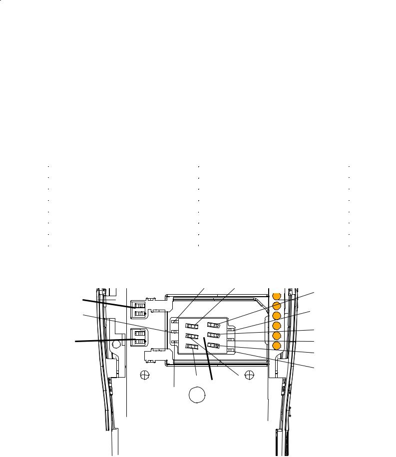
Bottom Connector
Microphone well
2, IMICP
D±cover to PCB gronund
3, IMICN
D±cover to PCB gronund
1
Charge_GND Mic sound port 4,5,6,7,8
13, V_charge_in Pad
Audio
Jack
10,11,12 Charger Jack 9, Charge_Ctrl, pad
Figure 3. Bottom Connector, X503, pin locations (top View)
Charge_GND |
Mic sound port |
|
Audio |
|
Charge_ctrl |
|
Charger Jack |
13, V_charge_in Pad |
||||||
|
Jack |
|
|
9 |
|
|
|
|
||||||
|
1 |
|
|
|
|
|
|
|
|
10,11,12 |
|
|
D±cover to |
|
|
|
|
|
|
4,5,6,7,8 |
|
|
|
|
|
||||
D±cover to |
|
|
|
|
|
|
|
|
|
|
||||
|
|
|
|
|
|
|
|
|
|
|
|
|
PCB GND |
|
PCB GND |
|
|
|
|
|
|
|
|
|
|
|
|
|
|
D±cover to |
1 |
2 |
15 |
3 15 |
4 |
|
6 |
|
8 |
9 |
11 |
12 |
|
D±cover to |
5 |
|
10 |
|
|||||||||||
PCB GND |
|
|
|
|
|
7 |
13 |
PCB GND |
||||||
|
|
|
|
|
|
|
|
|
|
|
|
|
|
|
|
|
|
Figure 4. |
Bottom Connector, X503, pin locations (BottomView) |
|
|||||||||
Issue 1 07/99 |
|
|
|
|
|
|
|
|
|
|
|
Page 2± 15 |
||

NSE±8/9 |
PAMS |
System Module |
Technical Documentation |
|
Table 10. Signals of the bottom connector X503
Pin |
Name |
Parameter |
Min |
Typ |
Max |
Unit |
Notes |
1, |
Charge |
Charger re- |
±0.3 |
|
0 |
V |
W.R.T GND |
10 |
_GND |
turn |
|
|
|
|
|
|
|
|
|
|
|
|
|
2 |
IMICP |
IMICP |
|
0.55 |
4.1 |
mV |
Connected to COBBA |
|
|
|
|
|
|
|
MIC2P/N input. The maxi- |
|
|
|
|
|
|
|
mum value corresponds to1 |
|
|
|
|
|
|
|
kHz, 0 dBmO network level |
3 |
IMICN |
IMICN |
|
0.55 |
4.1 |
mV |
|
|
with input amplifier gain set |
||||||
|
|
|
|
|
|
|
to 32 dB. typical value is |
|
|
|
|
|
|
|
maximum value ±16 dB. |
|
|
|
|
|
|
|
|
4 |
INT |
Headint low |
0.57 |
0.65 |
0.72 |
V |
No plug inserted in audio |
|
|
|
|
|
|
|
jack |
|
|
|
|
|
|
|
|
|
|
Headint high |
Vbbmin |
Vbb |
Vbbmax |
V |
Plug inserted in audio Jack |
|
|
|
|
|
|
|
|
5 |
XEarP |
positive line |
113 |
150 |
188 |
Ω |
Output AC impedance (ref. |
|
*) |
for external |
|
|
|
|
XEarN) HDC±5 |
|
audio output |
|
|
|
|
f<3400 Hz |
|
|
|
|
|
|
|
||
|
|
|
|
|
|
|
|
|
|
HDC±5 mode |
|
|
0.84 |
Vpp |
Output level (ref. XEarN) |
|
|
|
|
|
|
HDC±5 |
|
|
|
|
|
|
|
|
|
|
|
|
|
|
|
|
f<3400 Hz |
|
|
|
|
|
|
|
|
|
|
PPH±1 mode |
4.0 |
4.2 |
4.4 |
KΩ |
Output AC impedance (ref. |
|
|
|
|
|
|
|
XEarN) PPH±1 |
|
|
|
|
|
|
|
300< f<3400 Hz |
|
|
|
|
|
|
|
|
|
|
|
|
|
1.8 |
Vpp_ac |
Output level (ref. XEarN) |
|
|
|
|
|
|
|
PPH±1 |
|
|
|
|
|
|
|
f<3400 Hz |
|
|
|
|
|
|
|
|
Page 2± 16 |
Issue 1 07/99 |

PAMS |
NSE±8/9 |
|
|
Technical Documentation |
System Module |
|
Table 10. Signals of the bottom connector X503 (continued)
Pin |
Name |
Parameter |
Min |
Typ |
Max |
Unit |
Notes |
6 |
XMicN |
Negative line |
|
|
0.025 |
Vpp |
Maximum input signal level |
|
*) |
for external |
|
|
|
|
(ref. XMicP) with Cobba gain |
|
audio input |
|
|
|
|
18dB, |
|
|
|
|
|
|
|
||
|
|
to phone |
|
|
|
|
300< f <3400 Hz |
|
|
|
|
|
|
|
|
|
|
HDC±5 mode |
|
40 |
|
dB/dec |
Input attenuation, f<300 Hz |
|
|
|
|
|
|
(ref. XMicP) |
|
|
|
|
|
|
|
|
|
|
|
|
|
|
|
|
|
|
|
|
775 |
895 |
995 |
mV |
Hook active DC level ref. |
|
|
|
|
|
|
|
gnd |
|
|
|
|
|
|
|
|
|
|
|
95 |
|
380 |
mV |
Hook in±active DC level ref. |
|
|
|
|
|
|
|
gnd |
|
|
|
|
|
|
|
|
|
|
|
±100 |
|
±400 |
μA |
Bias current (ref. XMicP) |
|
|
|
|
|
|
|
|
|
|
PPH±1 mode |
|
|
0.5 |
Vpp |
Maximum input signal level |
|
|
|
|
|
|
|
(ref. XMicP) with Cobba gain |
|
|
|
|
|
|
|
12dB, |
|
|
|
|
|
|
|
300< f <3400 Hz |
|
|
|
|
|
|
|
|
|
|
|
|
20 |
|
dB/dec |
Input attenuation, f<300 Hz |
|
|
|
|
|
|
|
(ref. XMicP) |
|
|
|
|
|
|
|
|
|
|
|
2500 |
|
|
mV |
Mute (output DC level), wrt. |
|
|
|
|
|
|
|
Charge_gnd without |
|
|
|
|
|
|
|
HFM±8 |
|
|
|
|
|
|
|
|
|
|
|
2130 |
|
|
mV |
Mute (output DC level), wrt. |
|
|
|
|
|
|
|
Charge_gnd with HFM±8 |
|
|
|
|
|
|
|
|
|
|
|
|
|
2230 |
mV |
Unmute (output DC level), |
|
|
|
|
|
|
|
wrt. charge_ gnd without |
|
|
|
|
|
|
|
HFM±8 |
|
|
|
|
|
|
|
|
|
|
|
|
|
1850 |
mV |
Unmute (output DC level), |
|
|
|
|
|
|
|
wrt. charge_ gnd with |
|
|
|
|
|
|
|
HFM±8 |
|
|
|
|
|
|
|
|
7 |
XEarN |
Negative line |
|
|
|
|
See XEarP pin definitions |
|
*) |
for external |
|
|
|
|
output is symmetrical |
|
audio output |
|
|
|
|
|
|
|
|
|
|
|
|
|
|
|
|
HDC±5 mode |
|
|
|
|
|
|
|
|
|
|
|
|
|
|
|
PPH±1 mode |
|
|
|
|
See XEarP pin definitions |
|
|
|
|
|
|
|
output is symmetrical |
|
|
|
|
|
|
|
|
Issue 1 07/99 |
Page 2± 17 |

NSE±8/9 |
PAMS |
System Module |
Technical Documentation |
|
Table 10. Signals of the bottom connector X503 (continued)
Pin |
Name |
Parameter |
Min |
Typ |
Max |
Unit |
Notes |
8 |
XMicP |
Positive line |
|
|
0.025 |
Vpp |
Maximum input signal level |
|
*) |
for external |
|
|
|
|
(ref. XMicN) with Cobba gain |
|
|
audio input to |
|
|
|
|
18dB, |
|
|
phone |
|
|
|
|
300< f <3400 Hz |
|
|
|
|
|
|
|
|
|
|
HDC±5 mode |
|
40 |
|
dB/dec |
Attenuation of input inside |
|
|
|
|
|
|
phone, |
|
|
|
|
|
|
|
|
f<300 Hz (ref. XMicN) |
|
|
|
|
|
|
|
|
|
|
|
1450 |
|
2090 |
mV |
Headset identification DC |
|
|
|
|
|
|
|
level ref. gnd @ AUXout = |
|
|
|
|
|
|
|
2.1V and |
|
|
|
|
|
|
|
PDATA_4 =ºLº |
|
|
|
|
|
|
|
|
|
|
|
100 |
|
400 |
μA |
Bias current (ref. XMicN) |
|
|
|
|
|
|
|
|
|
|
PPH±1 |
|
|
0.5 |
Vpp |
Maximum input signal level |
|
|
|
|
|
|
|
(ref. XMicN) with Cobba gain |
|
|
|
|
|
|
|
12dB, |
|
|
|
|
|
|
|
300< f <3400 Hz |
|
|
|
|
|
|
|
|
|
|
|
|
20 |
|
dB/dec |
Input attenuation, f<300 Hz |
|
|
|
|
|
|
|
(ref. XMicN) |
|
|
|
|
|
|
|
|
|
|
|
2060 |
2180 |
2300 |
mV |
PPH±1 with HFM±8 identifi- |
|
|
|
|
|
|
|
cation DC level, wrt. |
|
|
|
|
|
|
|
Charge_gnd |
|
|
|
|
|
|
|
@ AUXout = ºZº and PDA- |
|
|
|
|
|
|
|
TA_4 =ºLº |
|
|
|
|
|
|
|
|
|
|
|
2490 |
2600 |
2720 |
mV |
PPH±1 with out HFM±8 |
|
|
|
|
|
|
|
identification DC level, wrt. |
|
|
|
|
|
|
|
Charge_gnd |
|
|
|
|
|
|
|
@ AUXout = ºZº and PDA- |
|
|
|
|
|
|
|
TA_4 =ºLº |
|
|
|
|
|
|
|
|
9, |
Charge |
PWM exter- |
0 |
|
0.5 |
V |
Charger control PWM low |
12 |
_Ctrl |
nal charge |
|
|
|
|
|
2.4 |
|
|
V |
Charger control PWM high |
|||
|
|
control |
|
|
|||
|
|
|
|
|
|
|
|
|
|
|
|
32 |
|
Hz |
PWM frequency for a 3 wire |
|
|
|
|
|
|
|
charger |
|
|
|
|
|
|
|
|
|
|
|
1 |
25 |
99 |
% |
PWM duty cycle |
|
|
|
|
|
|
|
|
Page 2± 18 |
Issue 1 07/99 |
PAMS |
NSE±8/9 |
|
|
Technical Documentation |
System Module |
|
Table 10. Signals of the bottom connector X503 (continued)
Pin |
Name |
Parameter |
Min |
Typ |
Max |
Unit |
Notes |
11. |
V_char |
Charger volt- |
7.25 |
7.6 |
7.95 |
Vrms |
Unloaded ACP±7 Charger |
13 |
ge_IN |
age input, |
|
11.1 |
16.9 |
Vp |
Unloaded Peak voltage |
|
|
|
|
||||
|
|
ACP±7 type |
320 |
370 |
420 |
mA |
Supply current |
|
|
|
|
|
1.1 |
Apeak |
Supply current |
|
|
|
|
|
|
|
|
|
|
ACP±8 type |
5.7 |
6.0 |
6.3 |
Vrms |
Unloaded ACP±8 Charger |
|
|
|
500 |
620 |
750 |
mA |
Supply current |
|
|
|
|
|
|
|
|
|
|
ACP±9 type |
7.1 |
8.4 |
9.3 |
Vrms |
Unloaded & charg_ctrl |
|
|
|
6.0 |
7.1 |
8.0 |
Vrms |
PWM= 0% |
|
|
|
Unloaded & charg_ctrl |
||||
|
|
|
720 |
800 |
850 |
mA |
|
|
|
|
PWM= 25% |
||||
|
|
|
|
|
|
|
|
|
|
|
|
|
|
|
Supply current |
|
|
|
|
|
|
|
|
15a |
Not |
Not used |
|
|
|
|
Internal short circuit in bot- |
15b |
used |
|
|
|
|
|
tom connector. Not used in |
|
|
|
|
|
|
|
NSE±8/9 |
|
|
|
|
|
|
|
|
16, |
Charge |
Charger re- |
± 0.3 |
|
0 |
V |
wrt. Supply ground |
17 |
_GND |
turn |
|
|
|
|
|
|
|
|
|
|
|
|
|
Speaker connection
Pad 1, EarN
Pad 2, EarP
Figure 5. Internal Speaker Pads
Issue 1 07/99 |
Page 2± 19 |
NSE±8/9 |
PAMS |
System Module |
Technical Documentation |
|
Table 11. Internal Earpiece connection, B201
Pad |
Name |
Min |
Typ |
Max |
Unit |
Remark |
1 |
EARN |
0 |
14 |
220 |
mVac |
Connected to COBBA_GJP EARN output. Typical level corre- |
|
|
|
|
|
|
sponds to ±16 dBmO network level with volume control giving |
|
|
|
|
|
|
nominal RLR (=+2dB) 8 db below max. Max level is 0dBmO |
|
|
|
|
|
|
with max volume (codec gain ±11 db) |
|
|
|
|
|
|
|
2 |
EARP |
0 |
14 |
220 |
mVac |
Connected to COBBA_GJP EARP output. Typical level corre- |
|
|
|
|
|
|
sponds to ±16 dBmO network level with volume control giving |
|
|
|
|
|
|
nominal RLR (=+2dB) 8 db below max. Max level is 0dBmO |
|
|
|
|
|
|
with max volume (codec gain ±11 db) |
|
|
|
|
|
|
|
Vibra motor connection
E104
E103
Figure 6. Vibra Motor±connetion pads
Page 2± 20 |
Issue 1 07/99 |
PAMS |
NSE±8/9 |
|
|
Technical Documentation |
System Module |
|
Table 12. Vibra motor connection, E103 & E104
Pad |
Name |
Min |
Typ |
Max |
Unit |
Comment |
E103 to E104 |
Rated voltage |
|
1.3 |
|
V |
|
|
|
|
|
|
|
|
E103 to E104 |
Rated current |
|
116 |
|
mA |
|
|
|
|
|
|
rms |
|
|
|
|
|
|
|
|
E103 to E104 |
Operating |
1.2 |
|
1.9 |
V rms |
|
|
voltage |
|
|
|
|
|
|
|
|
|
|
|
|
E103 to E104 |
Start voltage |
1.1 |
|
|
V rms |
|
|
|
|
|
|
|
|
E103 to E104 |
Start current |
|
|
135 |
mA |
|
|
|
|
|
|
rms |
|
|
|
|
|
|
|
|
E103 to E104 |
internal resis- |
|
10.7 |
|
ohm |
|
|
tance |
|
|
|
|
|
|
|
|
|
|
|
|
Internal Signals and Connections
This section describes all the signal between the Baseband blocks
Additionally the signals between the Baseband and the RF section are described.
|
|
Table 13. Audio Block connections |
|
|
|
Name |
Type |
Remark |
of signal |
|
|
charg_ctrl |
input |
connected for schematic reasons (use of TVS on audio sheet) |
|
|
|
HOOKDET |
output |
Logical signal indicating whether hook is active or not in accessory Low |
|
|
equals button activated. |
|
|
|
HEADDET |
output |
Logical output indicating whether the audio accessory is inserted (HIGH) |
|
|
or not (LOW). |
|
|
|
XEARP |
output |
Positive line of the external audio downlink signal. |
|
|
|
XEARN |
output |
Negative line of the external audio downlink signal. |
|
|
|
XMICP |
input |
Positive line of the external audio uplink signal |
|
|
|
XMICN |
input |
Negative line of the external audio uplink signal |
|
|
|
IMICP |
input |
Positive line of the internal microphone signal |
|
|
|
IMICN |
input |
Negative line of the internal microphone signal |
|
|
|
EAD |
output |
Analog voltage used for accessory identification. |
|
|
|
SERRFI(3:0) |
Bus |
Serial control for the COBBA_GJP and serial data for the RF interface. |
|
|
|
PCM(3:0) |
Bus |
Serial digital data for the COBBA_GJP audio |
|
|
|
COBBACLK |
input |
System clock for the COBBA_GJP |
|
|
|
COBBA |
input |
Reset signal to the COBBA_GJP |
RESET |
|
|
|
|
|
AFC |
output |
Analog voltage to RF controlling the system frequency |
|
|
|
RXC |
output |
Analog voltage for gain control in the RF±receiver (AGC) |
|
|
|
TXC |
output |
Analog voltage for the TX ramping control |
|
|
|
Issue 1 07/99 |
Page 2± 21 |

NSE±8/9 |
PAMS |
System Module |
Technical Documentation |
|
|
|
Table 13. Audio Block connections (continued) |
|
|
|
|
|
Name |
Type |
|
Remark |
of signal |
|
|
|
TXIN |
output |
|
Negative line of the in phase transmit signal |
|
|
|
|
TXIP |
output |
|
Positive line of the in phase transmit signal |
|
|
|
|
TXQN |
output |
|
Negative line of the quadrature phase transmit signal |
|
|
|
|
TXQP |
output |
|
Positive line of the quadrature phase transmit signal |
|
|
|
|
RXINP |
input |
|
Positive line of the in phase receive signal |
|
|
|
|
RXINN |
input |
|
Negative line of the in phase receive signal |
|
|
|
|
KEY_LIGHT |
output |
|
Logical signal controlling the keyboard backlight driver. |
|
|
|
|
LCD_LIGHT |
output |
|
Logical signal controlling the LCD backlight driver. |
|
|
|
|
|
|
Table 14. CPU connections |
|
|
|
Name |
Type |
Remark |
of signal |
|
|
PURX |
input |
Power on reset |
|
|
|
SLEEPCLK |
input |
32KHz sleep clock signal for MAD2PR1 operation in sleep state |
|
|
|
CCONTINT |
input |
Interrupt line from CCONT to MAD2PR1, for all events in CCONT |
|
|
|
HOOKDET |
Input |
Logical signal indicating whether the hook button of the accessory is acti- |
|
|
vated or not |
|
|
|
HEADDET |
input |
Logical signal indicating whether an accessory is inserted or not |
|
|
|
CCONTCSX |
output |
CCONT Chip select for the serial communication with MAD2PR1 |
|
|
|
MBUS |
bi |
Serial communication line between MAD2PR1 and external service or pro- |
|
direc- |
duction equipment. |
|
tional |
Clock line for F±bus communication during flashing. |
|
|
|
VIBRA |
output |
Logical output from MAD2PR1 to the vibra driver in the UISWITCH |
|
|
|
VCXOPWR |
output |
Control of power up/down of the 13MHz system clock, sleep mode control |
|
|
to CCONT |
|
|
|
SIMIF(4:0) |
bus |
Communication lines between MAD2PR1 and the SIM driver in CCONT |
|
|
|
GENSIO(1:0) |
bus |
Serial clock and data for the communication between MAD2PR1 and |
|
|
CCONT, and from MAD2PR1 to LCD±driver. |
|
|
|
CHARG_OFF |
output |
Logical signal controlling charging through PSCC, High disables start± |
|
|
and PWM±charging. |
|
|
|
PSCC_PWM |
output |
Logical signal controlling the charger switch inside PSCC, High switch |
|
|
open, Low switch closed |
|
|
|
FBUS_TX |
output |
Output for serial communication between MAD2PR1 and external service |
|
|
or production equipment. |
|
|
|
FBUS_RX |
input |
Input for serial communication between MAD2PR1 and external service or |
|
|
production equipment. |
|
|
|
SERFI(3:0) |
bus |
communication line between MAD2PR1 and COBBA_GJP for cobba con- |
|
|
trol and receive and transmit data for the RF transmission. |
|
|
|
Page 2± 22 |
Issue 1 07/99 |

PAMS |
NSE±8/9 |
|
|
Technical Documentation |
System Module |
|
|
|
Table 14. CPU connections (continued) |
|
|
|
Name |
Type |
Remark |
of signal |
|
|
PCM(3:0) |
bus |
communication line beteween MAD2PR1 and COBBA_GJP for receive |
|
|
and transmit data for the audio transmission. |
|
|
|
COBBACLK |
output |
13MHz clock for the synchronization COBBA |
|
|
|
COBBA |
output |
Reset signal from MAD2PR1 to Cobba_GJP |
RESET |
|
|
|
|
|
COL(3:0) |
output |
Column addresses for the keyboard scan |
|
|
|
ROW(4:0) |
input |
Row addresses from the keyboard scan and power±on key. |
|
|
|
BUZZER |
output |
PWM output from MAD2PR1 to the Buzzer driver in UISWITCH |
|
|
|
LCDCD |
output |
Control line to the LCD driver |
|
|
|
LCDEN |
output |
Chip select to the LCD driver |
|
|
|
LCDRSTX |
output |
Reset of the LCD driver |
|
|
|
VCON_1 |
output |
Least significant bit in the 2±bit DAC control of the DC/DC±converter out- |
|
|
put voltage. |
|
|
|
VCON_2 |
output |
Most significant bit in the 2±bit DAC control of the DC/DC±converter out- |
|
|
put voltage. |
|
|
|
LOW_BATT |
Input |
Battery removal alert to MAD2PR1 |
|
|
|
BTEMP |
Input |
connection to provide access to BTEMP signal in production and service |
|
|
|
SDATA |
output |
Serial data for the synthesizer inside SUMMA in the RF |
|
|
|
SCLK |
Output |
13/4 MHz clock for the serial communication with the synthesizer inside |
|
|
SUMMA in RF |
|
|
|
SENA1 |
output |
Chip select for the serial communication with SUMMA in RF |
|
|
|
FRACTRL |
output |
Controls signal for the gain in the LNA in the RF |
|
|
|
TXP |
output |
Logical control signal to indicate the power on of the TX circuitry |
|
|
|
RFC |
Input |
13MHz system clock from the RF |
|
|
|
BAND_SEL |
output |
Logical control of the band selection in the front end GSM 900 or DCS |
|
|
1800 |
|
|
|
|
|
Table 15. POWER connections |
|
|
|
Name |
Type |
Remark |
of signal |
|
|
V_CHARGE_IN |
input |
charger voltage input |
|
|
|
CHARGE_GND |
input |
charger current return |
|
|
|
CHARG_CTRL |
output |
Charger voltage control signal |
|
|
|
PSCC_PWM |
input |
Logical signal from MAD controlling the charger switch inside PSCC, |
|
|
High switch open, Low switch closed |
|
|
|
CHARG_OFF |
input |
Logical signal from MAD enabling / disabling charging through PSCC, |
|
|
High disables both start± and PWM±charging. |
|
|
|
Issue 1 07/99 |
Page 2± 23 |

NSE±8/9 |
PAMS |
System Module |
Technical Documentation |
|
|
Table 15. POWER connections (continued) |
|
|
|
|
Name |
Type |
Remark |
of signal |
|
|
GENSIO(1:0) |
bus |
Serial clock and data for communication between CCONT and |
|
|
MAD2PR1, and from MAD2PR1 to LCD±driver |
|
|
|
SIMIF(4:0) |
bus |
5 signals for MAD2PR1 communication with SIM through CCONT |
|
|
|
VCXOPWR |
input |
Control from MAD2PR1 to power on/off the 13 MHz oscillator, sleep |
|
|
mode control |
|
|
|
CCONTCSX |
input |
Chip select for communication with CCONT |
|
|
|
CCONTINT |
output |
Common CCONT event interrupt line to MAD2PR1 |
|
|
|
SLEEPCLK |
output |
32KHz clock for MAD2PR1 sleep mode operation |
|
|
|
PURX |
output |
Power up reset signal to MAD2PR1 |
|
|
|
VDC_out_2 |
output |
Filtered DC/DC output supply for Synth supply regulator in RF |
|
|
|
VRX_1 |
output |
Regulator output for Rx part of CRFU in RF |
|
|
|
VRX_2 |
output |
Regulator output for Rx part of SUMMA in RF |
|
|
|
VSYN_2 |
output |
Regulator output for VCO's and synthezeiser in SUMMA in RF |
|
|
|
VXO |
output |
Regulator output for 13 MHz oscillator in RF |
|
|
|
VTX |
output |
Regulator output for TX parts in SUMMA and CRFU in RF |
|
|
|
VCP |
output |
5v supply for SUMMA in RF |
|
|
|
VREF |
output |
1.5v common voltage reference for Baseband and RF |
|
|
|
VDC_OUT |
output |
DC/DC output supply voltage for PA's, backlight, vibra and buzzer |
|
|
|
RF_TEMP |
input |
Input from temperature sensor in RF |
|
|
|
TXP |
input |
TX burst synchronization |
|
|
|
LOW_BATT |
output |
Battery removal alert to MAD2PR1 |
|
|
|
EAD |
input |
external accessory detection, analog voltage to CCONT EAD ADC |
|
|
|
PWRON |
input |
Phone power on signal to CCONT, watch dog disable |
|
|
|
VCON_1 |
input |
DC/DC converter voltage control, LSB of two bit DAC |
|
|
|
VCON_2 |
input |
DC/DC converter voltage control, MSB of two bit DAC |
|
|
|
BTEMP |
output |
to test pad to provide access to BTEMP for production and service |
|
|
|
|
|
Table 16. UI connections |
|
|
|
Name |
Type |
Remark |
of signal |
|
|
WDDIS |
input |
Connection to panel connector in production for watch dog disable |
|
|
|
PWRON |
output |
Phone power on signal to CCONT |
|
|
|
COL(3:0) |
input |
Column addresses for the keyboard scan |
|
|
|
ROW(4:0) |
output |
Row addresses from the keyboard scan and power±on key. |
|
|
|
BUZZER |
input |
Logical input from MAD2PR1 to the Buzzer driver in UISWITCH |
|
|
|
LCDCD |
input |
Control line to the LCD driver |
|
|
|
Page 2± 24 |
Issue 1 07/99 |

PAMS |
NSE±8/9 |
|
|
Technical Documentation |
System Module |
|
|
|
Table 16. UI connections (continued) |
|
|
|
Name |
Type |
Remark |
of signal |
|
|
LCDEN |
input |
Chip select to the LCD driver |
|
|
|
LCDRSTX |
input |
Reset of the LCD driver |
|
|
|
VIBRA |
input |
PWM output from MAD2PR1 to the vibra driver in the UISWITCH |
|
|
|
KEY_LIGHT |
input |
Logical signal controlling the keyboard backlight driver in the UISwitch. |
|
|
|
LCD_LIGHT |
input |
Logical signal controlling the LCD backlight driver in the UISwitch. |
|
|
|
GENSIO(1:0) |
bus |
Serial clock and data for communication between CCONT and MAD2PR1, |
|
|
and from MAD2PR1 to LCD±driver |
|
|
|
RF control and interface
The interface signals between the Baseband and the RF section are shown below.
Table 17. Signals within the Baseband controlling the RF
Signal |
From |
Parameter |
Mini- |
Typi- |
Maxi- |
Unit |
Function |
name |
To |
|
mum |
cal |
mum |
|
|
SERRIF 0 |
MAD2PR1 |
Logic high º1º |
2.0 |
|
Vbb |
V |
Idata for RF |
|
COBBA |
|
|
|
|
|
|
|
bi± |
Logic low º0º |
0 |
|
0.4 |
V |
|
|
directional |
|
|
|
|
|
|
|
|
|
|
|
|
|
|
SERRIF 1 |
MAD2PR1 |
Logic high º1º |
2.0 |
|
Vbb |
V |
Qdata for RF |
|
COBBA |
|
|
|
|
|
|
|
bi± |
Logic low º0º |
0 |
|
0.4 |
V |
|
|
directional |
|
|
|
|
|
|
|
|
|
|
|
|
|
|
SERRIF 2 |
MAD2PR1 |
Logic high º1º |
2.0 |
|
Vbb |
V |
CSX, |
|
COBBA |
|
|
|
|
|
chip select for SERRFI |
|
Logic low º0º |
0 |
|
0.4 |
V |
||
|
|
BUS |
|||||
|
|
|
|||||
|
|
|
|
|
|
|
|
SERRIF 3 |
MAD2PR1 |
Logic high º1º |
2.0 |
|
Vbb |
V |
SD, control data for |
|
COBBA |
|
|
|
|
|
cobba |
|
Logic low º0º |
0 |
|
0.4 |
V |
||
|
|
|
|||||
|
|
|
|
|
|
|
|
COBBA- |
MAD2PR1 |
Logic high º1º |
2.0 |
|
Vbb |
V |
DSPGENOut5 |
RESET |
COBBA |
|
|
|
|
|
|
|
|
|
|
|
|
|
|
|
|
Logic low º0º |
0 |
|
0.4 |
V |
|
|
|
|
|
|
|
|
|
COBBA± |
MAD2PR1 |
Logic high º1º |
2.0 |
|
Vbb |
V |
|
CLK |
COBBA |
|
|
|
|
|
|
|
|
Logic low º0º |
0 |
|
0.4 |
V |
|
|
|
|
|
|
|
|
|
TXP |
MAD2PR1 |
Logic high º1º |
2.0 |
|
Vbb |
V |
|
|
CCONT |
|
|
|
|
|
|
|
|
|
|
|
|
|
|
|
|
Logic low º0º |
0 |
|
0.4 |
V |
|
|
|
|
|
|
|
|
|
Issue 1 07/99 |
Page 2± 25 |

NSE±8/9 |
PAMS |
System Module |
Technical Documentation |
|
Table 18. AC and DC Characteristics of signals between Baseband and RF
Signal |
From |
Parameter |
Mini- |
Typi- |
Maxi- |
Unit |
Function |
name |
To |
|
mum |
cal |
mum |
|
|
VRX_1 |
CCONT VR2 |
DC±voltage |
2.67 |
2.8 |
2.85 |
V |
for Rx part of CRFU |
|
CRFU3 |
|
|
|
|
|
|
|
voltage ripple |
|
10 |
15 |
mVpp |
|
|
|
|
|
|
||||
|
|
when on |
|
|
|
|
|
|
|
|
|
|
|
|
|
VRX_2 |
CCONT VR5 |
DC±voltage |
2.67 |
2.8 |
2.85 |
V |
for Rx part of Summa |
|
SUMMA |
|
|
|
|
|
|
|
voltage ripple |
|
5 |
15 |
mVpp |
|
|
|
|
|
|
||||
|
|
when on |
|
|
|
|
|
|
|
|
|
|
|
|
|
VSYN_2 |
CCONT VR4 |
DC±voltage |
2.67 |
2.8 |
2.85 |
V |
for VCO's & Synth. i |
|
VCO's |
|
|
|
|
|
Summa |
|
voltage ripple |
|
5 |
|
mVpp |
||
|
|
|
|
|
|||
|
|
|
|
|
|
|
|
VXO |
CCONT VR1 |
DC±voltage |
2.67 |
2.8 |
2.85 |
V |
for 13 MHz oscillator |
|
VCTCXO |
|
|
|
|
|
|
|
voltage ripple |
|
5 |
15 |
mVpp |
|
|
|
|
|
|
||||
|
|
|
|
|
|
|
|
VTX |
CCONT VR7 |
DC±voltage |
2.67 |
2.8 |
2.85 |
V |
for Tx in Summa & |
|
CRFU3 |
|
|
|
|
|
CRFU |
|
Current |
|
|
150 |
mA |
||
|
|
|
|
|
|||
|
|
|
|
|
|
|
|
|
|
voltage ripple |
|
5 |
15 |
mVpp |
|
|
|
when on |
|
|
|
|
|
|
|
|
|
|
|
|
|
VCP |
CCONT V5V |
DC±voltage |
4.8 |
5.0 |
5.2 |
|
for Summa |
|
SUMMA |
|
|
|
|
|
|
|
Current |
|
|
30 ± |
mA |
|
|
|
|
|
|
|
|||
|
|
|
|
|
Isim |
|
|
|
|
|
|
|
|
|
|
|
|
voltage ripple |
|
10 |
25 |
mVpp |
|
|
|
|
|
|
|
|
|
VREF |
CCONT |
DC±Voltage |
1.478 |
1.5 |
1.523 |
V |
Reference voltage for |
|
SUMMA |
|
|
|
|
|
SUMMA |
|
Current |
|
|
100 |
uA |
||
|
|
|
|
||||
|
|
|
|
|
|
|
|
|
|
voltage ripple |
|
5 |
10 |
mVpp |
|
|
|
|
|
|
|
|
|
Vdc_out |
DC/DC±con- |
DC±Voltage |
|
|
|
|
|
|
verter output |
|
|
|
|
|
|
|
to |
|
|
|
|
|
|
|
RF PA's |
|
|
|
|
|
|
|
|
|
|
|
|
|
|
RF_TEM |
RF |
voltage |
0 |
|
1.5 |
V |
|
P |
CCONT |
|
|
|
|
|
|
BB pull up to |
±5% |
47 |
+5 % |
Kohm |
|
||
|
|
|
|||||
|
|
Vref |
|
|
|
|
|
|
|
|
|
|
|
|
Ro = 47Kohm +/±10% |
|
|
RF pull down to |
|
47 |
|
Kohm |
|
|
|
gnd |
|
|
|
NTC |
Bo = 4050 +/±3% |
|
|
|
|
|
|
|
|
|
|
ADC resolution |
|
10 |
|
bits |
|
|
|
|
|
|
|
|
|
Page 2± 26 |
Issue 1 07/99 |

PAMS |
NSE±8/9 |
|
|
Technical Documentation |
System Module |
|
Table 18. AC and DC Characteristics of signals between Baseband and RF (continued)
Signal |
From |
Parameter |
Mini- |
Typi- |
Maxi- |
Unit |
Function |
name |
To |
|
mum |
cal |
mum |
|
|
|
|
|
|
|
|
|
|
AFC |
COBBA_GJP |
Voltage |
0.046 |
|
2.254 |
V |
Automatic frequency |
|
VCTCXO |
|
|
|
|
|
control signal for |
|
Resolution |
|
11 |
|
bits |
||
|
|
|
VCTCXO |
||||
|
|
|
|
|
|
|
|
|
|
Load resistance |
10 |
|
|
kohm |
|
|
|
(dynamic) |
|
|
|
|
|
|
|
|
|
|
|
|
|
|
|
Load resistance |
1 |
|
|
Mohm |
|
|
|
(static) |
|
|
|
|
|
|
|
|
|
|
|
|
|
|
|
Noise voltage |
|
|
500 |
uVrms |
10...10000Hz |
|
|
|
|
|
|
|
|
|
|
Settling time |
|
|
0.5 |
ms |
|
|
|
|
|
|
|
|
|
RXC |
COBBA_GJP |
Voltage Min |
0.12 |
|
0.18 |
V |
Receiver gain control |
|
SUMMA |
|
|
|
|
|
|
|
Voltage Max |
2.27 |
|
2.33 |
V |
|
|
|
|
|
|
|
|
|
|
|
|
Vout tempera- |
|
|
10 |
LSB |
|
|
|
ture dependence |
|
|
|
|
|
|
|
|
|
|
|
|
|
|
|
Source imped- |
|
|
200 |
ohm |
|
|
|
ance |
|
|
|
|
|
|
|
active state |
|
|
|
|
|
|
|
|
|
|
|
|
|
|
|
Source imped- |
|
grounded |
|
|
|
|
|
ance |
|
|
|
|
|
|
|
power down |
|
|
|
|
|
|
|
state |
|
|
|
|
|
|
|
|
|
|
|
|
|
|
|
Input resistance |
1 |
|
|
Mohm |
|
|
|
|
|
|
|
|
|
|
|
Input capaci- |
|
|
10 |
pF |
|
|
|
tance |
|
|
|
|
|
|
|
|
|
|
|
|
|
|
|
Settling time |
|
|
10 |
us |
|
|
|
|
|
|
|
|
|
|
|
Noise level |
|
|
500 |
uVrms |
0...200 kHz |
|
|
|
|
|
|
|
|
|
|
Resolution |
10 |
|
|
bits |
|
|
|
|
|
|
|
|
|
|
|
DNL |
|
|
+/±0.9 |
LSB |
|
|
|
|
|
|
|
|
|
|
|
INL |
|
|
+/± 4 |
LSB |
|
|
|
|
|
|
|
|
|
Issue 1 07/99 |
Page 2± 27 |

NSE±8/9 |
PAMS |
System Module |
Technical Documentation |
|
Table 18. AC and DC Characteristics of signals between Baseband and RF (continued)
Signal |
From |
Parameter |
Mini- |
Typi- |
Maxi- |
Unit |
Function |
name |
To |
|
mum |
cal |
mum |
|
|
|
|
|
|
|
|
|
|
TXC |
COBBA_GJP |
Voltage Min |
0.12 |
|
0.18 |
V |
Transmitter power con- |
|
SUMMA |
|
|
|
|
|
trol |
|
Voltage Max |
2.27 |
|
2.33 |
V |
||
|
|
|
|||||
|
|
|
|
|
|
|
|
|
|
Vout tempera- |
|
|
10 |
LSB |
|
|
|
ture dependence |
|
|
|
|
|
|
|
|
|
|
|
|
|
|
|
Source imped- |
|
|
200 |
ohm |
|
|
|
ance |
|
|
|
|
|
|
|
active state |
|
|
|
|
|
|
|
|
|
|
|
|
|
|
|
Source imped- |
|
high Z |
|
|
|
|
|
ance |
|
|
|
|
|
|
|
power down |
|
|
|
|
|
|
|
state |
|
|
|
|
|
|
|
|
|
|
|
|
|
|
|
Input resistance |
10 |
|
|
kohm |
|
|
|
|
|
|
|
|
|
|
|
Input capaci- |
|
|
10 |
pF |
|
|
|
tance |
|
|
|
|
|
|
|
|
|
|
|
|
|
|
|
Settling time |
|
|
10 |
us |
|
|
|
|
|
|
|
|
|
|
|
Noise level |
|
|
500 |
uVrms |
0...200 kHz |
|
|
|
|
|
|
|
|
|
|
Resolution |
10 |
|
|
bits |
|
|
|
|
|
|
|
|
|
|
|
DNL |
|
|
+/±0.9 |
LSB |
|
|
|
|
|
|
|
|
|
|
|
INL |
|
|
+/± 4 |
LSB |
|
|
|
|
|
|
|
|
|
|
|
Timing inaccura- |
|
|
1 |
us |
|
|
|
cy |
|
|
|
|
|
|
|
|
|
|
|
|
|
TXIN / |
COBBA_GJP |
Differential volt- |
1.022 |
1.1 |
1.18 |
Vpp |
Differential in±phase TX |
TXIP |
SUMMA |
age swing |
|
|
|
|
Baseband signal for the |
|
|
|
|
|
|
RF modulator |
|
|
|
DC level |
0.784 |
0.8 |
0.816 |
V |
|
|
|
|
|||||
|
|
|
|
|
|
|
|
|
|
Differential offset |
|
|
+/± |
mV |
|
|
|
voltage (cor- |
|
|
2.0 |
|
|
|
|
rected) |
|
|
|
|
|
|
|
|
|
|
|
|
|
|
|
Diff. offset volt- |
|
|
+/± |
mV |
|
|
|
age temp. de- |
|
|
1.0 |
|
|
|
|
pendence |
|
|
|
|
|
|
|
|
|
|
|
|
|
|
|
Source imped- |
|
|
200 |
ohm |
|
|
|
ance |
|
|
|
|
|
|
|
|
|
|
|
|
|
|
|
Load resistance |
40 |
|
|
kohm |
|
|
|
|
|
|
|
|
|
|
|
Load capaci- |
|
|
10 |
pF |
|
|
|
tance |
|
|
|
|
|
|
|
|
|
|
|
|
|
|
|
DNL |
|
|
+/± |
LSB |
|
|
|
|
|
|
0.9 |
|
|
|
|
|
|
|
|
|
|
|
|
INL |
|
|
+/±1 |
LSB |
|
|
|
|
|
|
|
|
|
|
|
Group delay mis- |
|
|
100 |
ns |
|
|
|
smatch |
|
|
|
|
|
|
|
|
|
|
|
|
|
Page 2± 28 |
Issue 1 07/99 |

PAMS |
NSE±8/9 |
|
|
Technical Documentation |
System Module |
|
Table 18. AC and DC Characteristics of signals between Baseband and RF (continued)
Signal |
From |
Parameter |
Mini- |
Typi- |
Maxi- |
Unit |
Function |
name |
To |
|
mum |
cal |
mum |
|
|
|
|
|
|
|
|
|
|
TXQN / |
COBBA_GJP |
Differential volt- |
1.022 |
1.1 |
1.18 |
Vpp |
Differential quadrature |
TXQP |
SUMMA |
age swing |
|
|
|
|
phase TX Baseband |
|
|
|
|
|
|
signal for the RF modu- |
|
|
|
DC level |
0.784 |
0.8 |
0.816 |
V |
|
|
|
lator |
|||||
|
|
|
|
|
|
|
|
|
|
Differential offset |
|
|
+/± |
mV |
|
|
|
voltage (cor- |
|
|
2.0 |
|
|
|
|
rected) |
|
|
|
|
|
|
|
|
|
|
|
|
|
|
|
Diff. offset volt- |
|
|
+/± |
mV |
|
|
|
age temp. de- |
|
|
1.0 |
|
|
|
|
pendence |
|
|
|
|
|
|
|
|
|
|
|
|
|
|
|
Source imped- |
|
|
200 |
ohm |
|
|
|
ance |
|
|
|
|
|
|
|
|
|
|
|
|
|
|
|
Load resistance |
40 |
|
|
kohm |
|
|
|
|
|
|
|
|
|
|
|
Load capaci- |
|
|
10 |
pF |
|
|
|
tance |
|
|
|
|
|
|
|
|
|
|
|
|
|
|
|
Resolution |
8 |
|
|
bits |
|
|
|
|
|
|
|
|
|
|
|
DNL |
|
|
+/± |
LSB |
|
|
|
|
|
|
0.9 |
|
|
|
|
|
|
|
|
|
|
|
|
INL |
|
|
+/±1 |
LSB |
|
|
|
|
|
|
|
|
|
|
|
Group delay mis- |
|
|
100 |
ns |
|
|
|
smatch |
|
|
|
|
|
|
|
|
|
|
|
|
|
RXIP/ |
SUMMA |
Output level |
|
50 |
1344 |
mVpp |
Differential RX 13 MHz |
RXIN |
COBBA_GJP |
|
|
|
|
|
signal to Baseband |
Source imped- |
|
|
tbd. |
ohm |
|||
|
|
|
|
||||
|
|
ance |
|
|
|
|
|
|
|
|
|
|
|
|
|
|
|
Load resistance |
|
1 |
|
Mohm |
|
|
|
|
|
|
|
|
|
|
|
Load capaci- |
|
|
tbd. |
pF |
|
|
|
tance |
|
|
|
|
|
|
|
|
|
|
|
|
|
SDATA |
MAD2PR1 |
Logic high º1º |
2.0 |
|
Vbb |
V |
PLL data |
|
SUMMA |
|
|
|
|
|
|
|
Logic low º0º |
0 |
|
0.5 |
V |
|
|
|
|
|
|
|
|
|
|
|
|
Load impedance |
10 |
|
|
kohm |
|
|
|
|
|
|
|
|
|
|
|
Load capaci- |
|
|
10 |
pF |
|
|
|
tance |
|
|
|
|
|
|
|
|
|
|
|
|
|
|
|
Data rate fre- |
|
3.25 |
|
MHz |
|
|
|
quency |
|
|
|
|
|
|
|
|
|
|
|
|
|
Issue 1 07/99 |
Page 2± 29 |

NSE±8/9 |
PAMS |
System Module |
Technical Documentation |
|
Table 18. AC and DC Characteristics of signals between Baseband and RF (continued)
Signal |
From |
Parameter |
Mini- |
Typi- |
Maxi- |
Unit |
Function |
name |
To |
|
mum |
cal |
mum |
|
|
|
|
|
|
|
|
|
|
SCLK |
MAD2PR1 |
Logic high º1º |
2.0 |
|
Vbb |
V |
PLL clock |
|
SUMMA |
|
|
|
|
|
|
|
Logic low º0º |
0 |
|
0.5 |
V |
|
|
|
|
|
|
|
|
|
|
|
|
Load impedance |
10 |
|
|
kohm |
|
|
|
|
|
|
|
|
|
|
|
Load capaci- |
|
|
10 |
pF |
|
|
|
tance |
|
|
|
|
|
|
|
|
|
|
|
|
|
|
|
Data rate fre- |
|
3.25 |
|
MHz |
|
|
|
quency |
|
|
|
|
|
|
|
|
|
|
|
|
|
SENA1 |
MAD2PR1 |
Logic high º1º |
2.0 |
|
Vbb |
V |
PLL enable |
|
SUMMA |
|
|
|
|
|
|
|
Logic low º0º |
0 |
|
0.5 |
V |
|
|
|
|
|
|
|
|
|
|
|
|
Current |
|
|
50 |
uA |
|
|
|
|
|
|
|
|
|
|
|
Load capaci- |
|
|
10 |
pF |
|
|
|
tance |
|
|
|
|
|
|
|
|
|
|
|
|
|
FRACT |
MAD2PR1 |
Logic high º1º |
2.0 |
|
Vbb |
V |
Nominal gain in LNA |
RL |
CRFU |
|
|
|
|
|
|
Logic low º0º |
0 |
|
0.4 |
V |
Reduced gain in LNA |
||
|
|
||||||
|
|
|
|
|
|
|
|
|
|
Current |
|
|
0.1 |
mA |
|
|
|
|
|
|
|
|
|
TXP |
MAD2PR1 |
Logic high º1º |
2.0 |
|
Vbb |
V |
Transmitter power con- |
|
SUMMA |
|
|
|
|
|
trol enable |
|
Logic low º0º |
0 |
|
0.5 |
V |
||
|
|
|
|||||
|
|
|
|
|
|
|
|
|
|
Load Resistance |
50 |
|
|
kohm |
|
|
|
|
|
|
|
|
|
|
|
Load Capaci- |
|
|
10 |
pF |
|
|
|
tance |
|
|
|
|
|
|
|
|
|
|
|
|
|
|
|
Timing inaccura- |
|
|
1 |
us |
|
|
|
cy |
|
|
|
|
|
|
|
|
|
|
|
|
|
RFC |
VC(TC)XO |
Frequency |
|
13 |
|
MHz |
High stability clock sig- |
|
MAD2PR1 |
|
|
|
|
|
nal for the logic circuits |
|
Signal amplitude |
0.5 |
1.0 |
2.0 |
Vpp |
||
|
|
||||||
|
|
|
|
|
|
|
|
|
|
Load resistance |
10 |
|
|
kohm |
|
|
|
|
|
|
|
|
|
|
|
Load capaci- |
|
|
10 |
pF |
|
|
|
tance |
|
|
|
|
|
|
|
|
|
|
|
|
|
BAND_ |
MAD2PR1 |
Logic high º1º |
2.0 |
|
Vbb |
V |
GSM900 DSPGenOut 4 |
SEL |
CRFU 3 |
|
|
|
|
|
|
Logic low º0º |
0 |
|
0.4 |
V |
GSM1800 |
||
|
|
|
|||||
|
|
|
|
|
|
|
|
|
|
Current |
|
|
0.1 |
mA |
|
|
|
|
|
|
|
|
|
NOTE: Logic controls in low state when RF in power off.
Page 2± 30 |
Issue 1 07/99 |
Loading...