

DATA SHEET
PHOTOCOUPLER
PS2801C-1,PS2801C-4
HIGH ISOLATION VOLTAGE
SSOP PHOTOCOUPLER
DESCRIPTION
The PS2801C-1 and PS2801C-4 are optically coupled isolators containing a GaAs light emitting diode and an NPN
silicon phototransistor in a plastic SSOP for high density applications to realize an excellent cost performance.
This package has shield effect to cut off ambient light.
FEATURES
• High isolation voltage (BV = 2 500 Vr.m.s.)
• Small and thin package (4, 16-pin SSOP, Pin pitch 1.27 mm)
• V
CEO : 80 V
• Ordering number of tape product: PS2801C-1-F3, F4, PS2801C-4-F3, F4
• Pb-Free product
• Safety standards
• UL approved: File No. E72422
• DIN EN60747-5-2 (VDE0884 Part2) approved (Option)
APPLICATIONS
• Programmable logic controllers
• Measuring instruments
• Power supply
• Hybrid IC
PIN CONNECTION
−NEPOC Series−
(Top View)
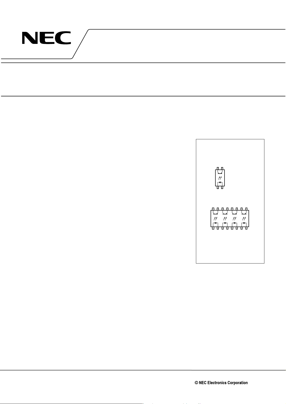
PS2801C-1
43
1. Anode
2. Cathode
3. Emitter
4. Collector
12
PS2801C-4
1615 14 13 12 11 10 9
12345678
1. 3. 5. 7.
2. 4. 6. 8.
9. 11. 13. 15.
10. 12. 14. 16.
Anode
Cathode
Emitter
Collector
The information in this document is subject to change without notice. Before using this document, please
confirm that this is the latest version.
Not all products and/or types are available in every country. Please check with an NEC Electronics
sales representative for availability and additional information.
Document No. PN10610EJ01V0DS (1st edition)
Date Published May 2006 NS CP(K)
Printed in Japan
2006
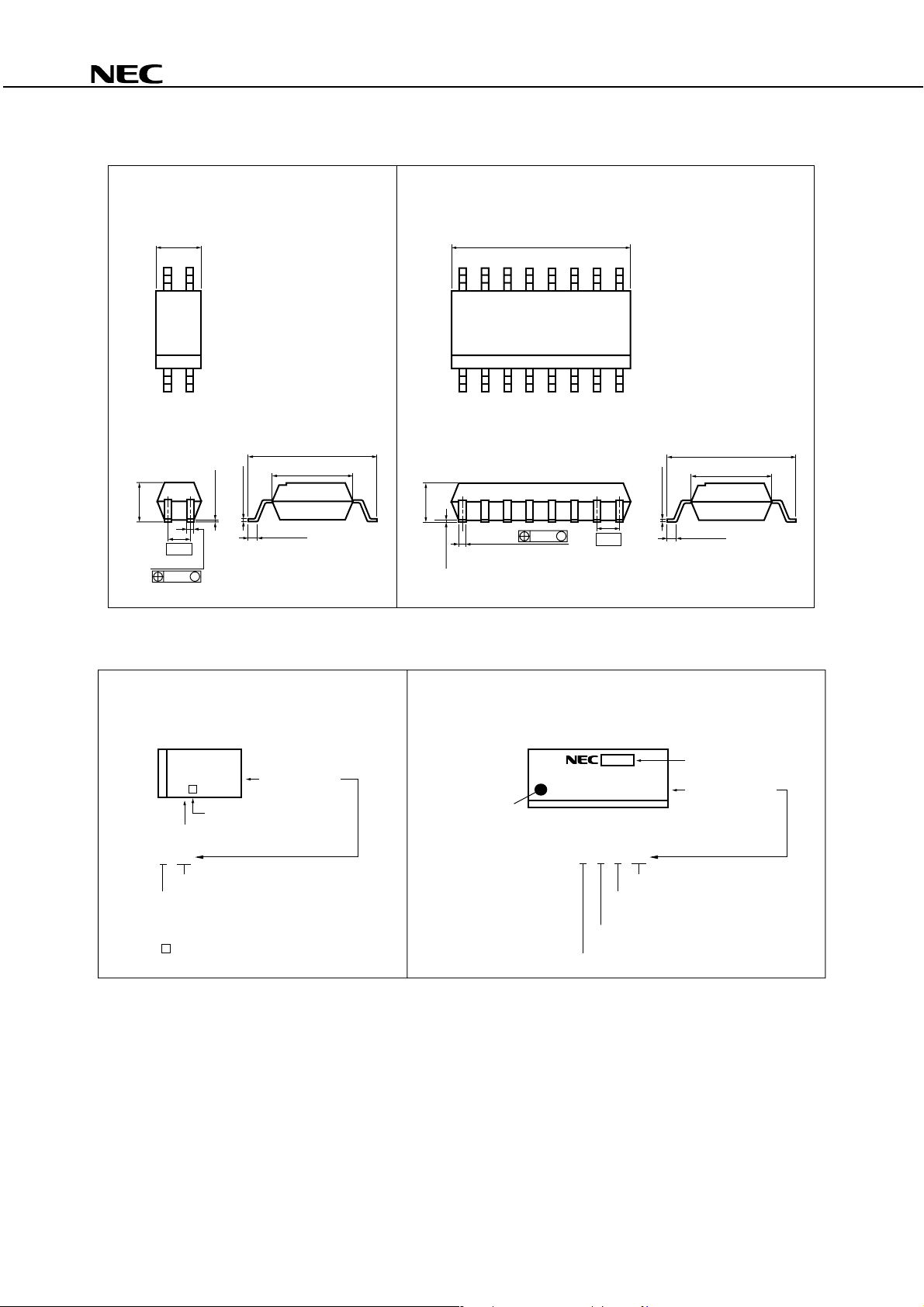
PACKAGE DIMENSIONS (UNIT: mm)
PS2801C-1,PS2801C-4
PS2801C-1
2.7±0.3
4
3
1
2
–0.05
+0.10
0.1±0.1
2.0±0.1
0.4±0.1
1.27
0.12
M
0.15
MARKING EXAMPLE
7.0±0.3
0.5±0.3
4.4
+0.3
–0.2
2.0
16
1
0.1±0.1
0.40
+0.10
–0.05
10.3±0.3
0.12
PS2801C-4
9
8
M
1.27
–0.05
+0.10
0.15
7.0±0.3
4.4
0.5±0.3
6 03
Year Assembled
(Last 1 Digit)
*1 : Pb-Free
PS2801C-1
1C
603
*1
Last number of type No. : 1C
Week Assembled
Assembly Lot
No. 1 pin
Mark
PS2801C-4
PS2801C-4
NL603
LN
6
Year Assembled
(Last 1 Digit)
In-house Code
(L: Pb-Free)
Rank Code
Country Assembled
Assembly Lot
03
Week Assembled
2
Data Sheet PN10610EJ01V0DS

PS2801C-1,PS2801C-4
ORDERING INFORMATION
Part Number Order Number
PS2801C-1 PS2801C-1-A Pb-Free 50 pcs (Tape 50 pcs cut) Standard products PS2801C-1
PS2801C-1-F3 PS2801C-1-F3-A Embossed Tape 3 500 pcs/reel (UL approved)
PS2801C-1-F4 PS2801C-1-F4-A
PS2801C-4 PS2801C-4-A Magazine Case 45 pcs PS2801C-4
PS2801C-4-F3 PS2801C-4-F3-A Embossed Tape 2 500 pcs/reel
PS2801C-4-F4 PS2801C-4-F4-A
PS2801C-1-V PS2801C-1-V-A 50 pcs (Tape 50 pcs cut) DIN EN60747-5-2 PS2801C-1
PS2801C-1-V-F3 PS2801C-1-V-F3-A Embossed Tape 3 500 pcs/reel (VDE0884 Part2)
PS2801C-1-V-F4 PS2801C-1-V-F4-A Approved (Option)
PS2801C-4-V PS2801C-4-V-A Magazine Case 45 pcs PS2801C-4
PS2801C-4-V-F3 PS2801C-4-V-F3-A Embossed Tape 2 500 pcs/reel
PS2801C-4-V-F4 PS2801C-4-V-F4-A
Solder Plating
Specification
Packing Style
*1 For the application of the Safety Standard, following part number should be used.
Safety Standard
Approval
Application Part
Number
*1
Data Sheet PN10610EJ01V0DS
3
PS2801C-1,PS2801C-4
ABSOLUTE MAXIMUM RATINGS (TA = 25°C, unless otherwise specified)
Parameter Symbol Ratings Unit
Diode Forward Current (DC) IF 30 mA/ch
Reverse Voltage VR 6 V
Power Dissipation Derating
Power Dissipation PD 60 80 mW/ch
Peak Forward Current
Transistor Collector to Emitter Voltage VCEO 80 V
Emitter to Collector Voltage VECO 5 V
Collector Current IC 30 mA/ch
Power Dissipation Derating
Power Dissipation PC 120 mW/ch
Isolation Voltage
Operating Ambient Temperature TA −55 to +100 °C
Storage Temperature Tstg −55 to +150 °C
*2
BV 2 500 Vr.m.s.
*1
IFP 0.5 A/ch
∆
PD/°C 0.6 0.8 mW/°C
∆
PC/°C 1.2 mW/°C
PS2801C-1 PS2801C-4
*1 PW = 100
*2 AC voltage for 1 minute at T
µ
s, Duty Cycle = 1%
A = 25°C, RH = 60% between input and output
Pins 1-2 shorted together, 3-4 shorted together (PS2801C-1).
Pins 1-8 shorted together, 9-16 shorted together (PS2801C-4).
4
Data Sheet PN10610EJ01V0DS

PS2801C-1,PS2801C-4
ELECTRICAL CHARACTERISTICS (TA = 25°C)
Parameter Symbol Conditions MIN. TYP. MAX. Unit
Diode Forward Voltage VF IF = 5 mA 1.2 1.4 V
Reverse Current IR VR = 5 V 5
Terminal Capacitance Ct V = 0 V, f = 1.0 MHz 10 pF
Transistor
Coupled
Isolation Resistance RI-O VI-O = 1.0 kVDC 1011
Isolation Capacitance CI-O V = 0 V, f = 1.0 MHz 0.4 pF
Rise Time
Fall Time
*1 CTR rank
N : 50 to 400 (%)
P : 150 to 300 (%)
L : 100 to 300 (%)
M : 100 to 400 (%)
N : 50 to 400 (%)
M : 100 to 400 (%)
*2 Test circuit for switching time
Pulse Input
Collector to Emitter Dark
Current
Current Transfer Ratio
*1
C/IF)
(I
Collector Saturation
Voltage
*2
tr VCC = 5 V, IC = 2 mA, RL = 100 Ω 5 µs
*2
tf 7
PS2801C-1
PS2801C-4
ICEO VCE = 80 V, IF = 0 mA 100 nA
CTR I
F = 5 mA, VCE = 5 V 50 400 %
VCE (sat) IF = 10 mA, IC = 2 mA 0.13 0.3 V
V
CC
µ
A
Ω
PW = 100 s
µ
Duty Cycle = 1/10
I
F
50 Ω
V
OUT
RL = 100 Ω
Data Sheet PN10610EJ01V0DS
5

TYPICAL CHARACTERISTICS (TA = 25°C, unless otherwise specified)
DIODE POWER DISSIPATION vs.
AMBIENT TEMPERATURE
100
(mW)
80
D
60
PS2801C-1
40
20
Diode Power Dissipation P
0
0 25 50 75 100 125
Ambient Temperature T
PS2801C-4
0.6 mW/˚C
0.8 mW/˚C
A
(˚C)
TRANSISTOR POWER DISSIPATION
vs. AMBIENT TEMPERATURE
200
(mW)
C
160
120
80
40
Transistor Power Dissipation P
0
0 25 50 75 100 125
Ambient Temperature T
PS2801C-1,PS2801C-4
PS2801C-1
PS2801C-4
1.2 mW/˚C
A
(˚C)
FORWARD CURRENT vs.
FORWARD VOLTAGE
100
50
(mA)
10
F
5
1
0.5
Forward Current I
0.1
0.05
T
A
= +100˚C
+60˚C
+25˚C
Forward Voltage VF (V)
–25˚C
–55˚C
COLLECTOR TO EMITTER DARK
CURRENT vs. AMBIENT TEMPERATURE
10 000
(nA)
CEO
1 000
100
VCE = 80 V
70 V
24 V
0˚C
COLLECTOR CURRENT vs.
COLLECTOR TO EMITTER VOLTAGE
30
CTR = 250%
25
(mA)
C
20
15
10
Collector Current I
5
0
1.51.41.31.21.11.00.90.80.7
0246810
Collector to Emitter Voltage V
IF = 10 mA
5 mA
2 mA
1 mA
CE
(V)
COLLECTOR CURRENT vs.
COLLECTOR SATURATION VOLTAGE
10
(mA)
C
1
IF = 10 mA
5 mA
2 mA
1 mA
10
1
Collector to Emitter Dark Current I
0 25 50 75 100
Ambient Temperature TA (˚C)
CTR = 200%
Remark The graphs indicate nominal characteristics.
6
Data Sheet PN10610EJ01V0DS
Collector Current I
0.1
0 0.2 0.4 0.6 0.8 1.0
Collector Saturation Voltage V
CTR = 250%
CE(sat)
(V)

PS2801C-1,PS2801C-4
NORMALIZED CURRENT TRANSFER
RATIO vs. AMBIENT TEMPERATURE
1.4
CTR = 250%
1.2
1.0
0.8
80%
0.6
0.4
Normalized to 1.0
0.2
at T
A
= 25˚C,
F
= 5 mA, VCE = 5 V
I
Normalized Current Transfer Ratio CTR
0
–
50
–7
5
–
25 0 25 7550 100
Ambient Temperature T
A
(˚C)
SWITCHING TIME vs.
LOAD RESISTANCE
100
IC = 2 mA, VCC = 5 V,
CTR = 228%
t
f
µ
10
tr
t
d
CURRENT TRANSFER RATIO vs.
FORWARD CURRENT
400
VCE = 5 V,
n = 3
300
Sample A
200
B
C
100
Current Transfer Ratio CTR (%)
0
0.01 0.1 1 10 100
Forward Current I
F
(mA)
SWITCHING TIME vs.
LOAD RESISTANCE
1 000
IF = 5 mA, VCC = 5 V,
CTR = 228%
t
µ
100
f
t
s
t
1
s
Switching Time t ( s)
0.1
10 100 1 000 10 000
Load Resistance RL (Ω)
FREQUENCY RESPONSE
5
0
–
5
RL = 1 kΩ
–
10
–
15
Normalized Gain Gv
–
20
IF = 5 mA,
V
CE
–
= 5 V
25
0.1 1
10
Frequency f (kHz)
Remark The graphs indicate nominal characteristics.
100 Ω
300 Ω
100 1 000
10
Switching Time t ( s)
t
r
t
1
1 10 100
d
Load Resistance RL (kΩ)
LONG TERM CTR DEGRADATION
1.2
1.0
0.8
0.6
0.4
CTR (Relative Value)
0.2
0
10
IF = 5 mA,
IF = 20 mA,
IF = 5 mA,
2
10
TA = 25˚C
TA = 25˚C
TA = 60˚C
3
10
Time (Hr)
10
4
TYP.
10
5
Data Sheet PN10610EJ01V0DS
7

TAPING SPECIFICATIONS (UNIT: mm)
Outline and Dimensions (Tape)
2.0±0.1
4.0±0.1
1.55±0.1
4.0±0.1
Tape Direction
1.5
φ
2.85±0.1
+0.1
–0
1.75±0.1
7.5±0.1
PS2801C-1,PS2801C-4
2.8 MAX.
7.55±0.1
16.0±0.3
0.3
2.3±0.1
PS2801C-1-F3 PS2801C-1-F4
1C
603
6031C603
1C
1C
1C
603
603
Outline and Dimensions (Reel)
R 1.0
2.0±0.5
13.0±0.2
φ
φ
21.0±0.8
6031C6031C6031C603
603
1C
1C
330±2.0
φ
100±1.0
φ
2.0±0.5
17.5±1.0
21.5±1.0
8
15.9 to 19.4
Packing: 3 500 pcs/reel
Outer edge of
flange
Data Sheet PN10610EJ01V0DS

Outline and Dimensions (Tape)
PS2801C-1,PS2801C-4
2.0±0.1
4.0±0.1
1.55±0.1
12.0±0.1
Tape Direction
+0.1
1.5
φ
–0
8.3±0.1
PS2801C-4-F3 PS2801C-4-F4
1.75±0.1
7.5±0.1
16.0±0.3
10.7±0.1
2.8 MAX.
0.3
2.3±0.1
Outline and Dimensions (Reel)
2.0±0.5
2.0±0.5
13.0±0.2
φ
330±2.0
R 1.0
Packing: 2 500 pcs/reel
21.0±0.8
φ
φ
100±1.0
φ
17.5±1.0
21.5±1.0
15.9 to 19.4
Outer edge of
flange
Data Sheet PN10610EJ01V0DS
9

PS2801C-1,PS2801C-4
NOTES ON HANDLING
1. Recommended soldering conditions
(1) Infrared reflow soldering
• Peak reflow temperature 260°C or below (package surface temperature)
• Time of peak reflow temperature 10 seconds or less
• Time of temperature higher than 220°C 60 seconds or less
• Time to preheat temperature from 120 to 180°C 120±30 s
• Number of reflows Three
• Flux Rosin flux containing small amount of chlorine (The flux with a
maximum chlorine content of 0.2 Wt% is recommended.)
Recommended Temperature Profile of Infrared Reflow
(heating)
to 10 s
260˚C MAX.
220˚C
to 60 s
180˚C
120˚C
Package Surface Temperature T (˚C)
120±30 s
(preheating)
Time (s)
(2) Wave soldering
• Temperature 260°C or below (molten solder temperature)
• Time 10 seconds or less
• Preheating conditions 120°C or below (package surface temperature)
• Number of times One (Allowed to be dipped in solder including plastic mold portion.)
• Flux Rosin flux containing small amount of chlorine (The flux with a maximum chlorine
content of 0.2 Wt% is recommended.)
(3) Soldering by Soldering Iron
• Peak Temperature (lead part temperature) 350°C or below
• Time (each pins) 3 seconds or less
• Flux Rosin flux containing small amount of chlorine (The flux with a
maximum chlorine content of 0.2 Wt% is recommended.)
(a) Soldering of leads should be made at the point 1.5 to 2.0 mm from the root of the lead
(b) Please be sure that the temperature of the package would not be heated over 100°C
10
Data Sheet PN10610EJ01V0DS

PS2801C-1,PS2801C-4
(4) Cautions
• Fluxes
Avoid removing the residual flux with freon-based and chlorine-based cleaning solvent.
2. Cautions regarding noise
Be aware that when voltage is applied suddenly between the photocoupler’s input and output or between
collector-emitters at startup, the output transistor may enter the on state, even if the voltage is within the absolute
maximum ratings.
3. Measurement conditions of current transfer ratios (CTR), which differ according to photocoupler
Check the setting values before use, since the forward current conditions at CTR measurement differ according
to product.
When using products other than at the specified forward current, the characteristics curves may differ from the
standard curves due to CTR value variations or the like. This tendency may sometimes be obvious, especially
below I
F = 1 mA.
Therefore, check the characteristics under the actual operating conditions and thoroughly take variations or the
like into consideration before use.
USAGE CAUTIONS
1. Protect against static electricity when handling.
2. Avoid storage at a high temperature and high humidity.
Data Sheet PN10610EJ01V0DS
11

PS2801C-1,PS2801C-4
•
The information in this document is current as of May, 2006. The information is subject to change
without notice. For actual design-in, refer to the latest publications of NEC Electronics data sheets or
data books, etc., for the most up-to-date specifications of NEC Electronics products. Not all
products and/or types are available in every country. Please check with an NEC Electronics sales
representative for availability and additional information.
No part of this document may be copied or reproduced in any form or by any means without the prior
•
written consent of NEC Electronics. NEC Electronics assumes no responsibility for any errors that may
appear in this document.
•
NEC Electronics does not assume any liability for infringement of patents, copyrights or other intellectual
property rights of third parties by or arising from the use of NEC Electronics products listed in this document
or any other liability arising from the use of such products. No license, express, implied or otherwise, is
granted under any patents, copyrights or other intellectual property rights of NEC Electronics or others.
Descriptions of circuits, software and other related information in this document are provided for illustrative
•
purposes in semiconductor product operation and application examples. The incorporation of these
circuits, software and information in the design of a customer's equipment shall be done under the full
responsibility of the customer. NEC Electronics assumes no responsibility for any losses incurred by
customers or third parties arising from the use of these circuits, software and information.
•
While NEC Electronics endeavors to enhance the quality, reliability and safety of NEC Electronics products,
customers agree and acknowledge that the possibility of defects thereof cannot be eliminated entirely. To
minimize risks of damage to property or injury (including death) to persons arising from defects in NEC
Electronics products, customers must incorporate sufficient safety measures in their design, such as
redundancy, fire-containment and anti-failure features.
•
NEC Electronics products are classified into the following three quality grades: "Standard", "Special" and
"Specific".
The "Specific" quality grade applies only to NEC Electronics products developed based on a customerdesignated "quality assurance program" for a specific application. The recommended applications of an NEC
Electronics product depend on its quality grade, as indicated below. Customers must check the quality grade of
each NEC Electronics product before using it in a particular application.
"Standard":
"Special":
"Specific":
Computers, office equipment, communications equipment, test and measurement equipment, audio
and visual equipment, home electronic appliances, machine tools, personal electronic equipment
and industrial robots.
Transportation equipment (automobiles, trains, ships, etc.), traffic control systems, anti-disaster
systems, anti-crime systems, safety equipment and medical equipment (not specifically designed
for life support).
Aircraft, aerospace equipment, submersible repeaters, nuclear reactor control systems, life
support systems and medical equipment for life support, etc.
The quality grade of NEC Electronics products is "Standard" unless otherwise expressly specified in NEC
Electronics data sheets or data books, etc. If customers wish to use NEC Electronics products in applications
not intended by NEC Electronics, they must contact an NEC Electronics sales representative in advance to
determine NEC Electronics' willingness to support a given application.
(Note)
(1)
"NEC Electronics" as used in this statement means NEC Electronics Corporation and also includes its
majority-owned subsidiaries.
(2)
"NEC Electronics products" means any product developed or manufactured by or for NEC Electronics (as
defined above).
12
Data Sheet PN10610EJ01V0DS
M8E 02. 11-1

Caution GaAs Products
PS2801C-1,PS2801C-4
This product uses gallium arsenide (GaAs).
GaAs vapor and powder are hazardous to human health if inhaled or ingested, so please observe
the following points.
• Follow related laws and ordinances when disposing of the product. If there are no applicable laws
and/or ordinances, dispose of the product as recommended below.
1. Commission a disposal company able to (with a license to) collect, transport and dispose of
materials that contain arsenic and other such industrial waste materials.
2. Exclude the product from general industrial waste and household garbage, and ensure that the
product is controlled (as industrial waste subject to special control) up until final disposal.
• Do not burn, destroy, cut, crush, or chemically dissolve the product.
• Do not lick the product or in any way allow it to enter the mouth.
For further information, please contact
NEC Compound Semiconductor Devices Hong Kong Limited
E-mail: contact@ncsd-hk.necel.com
Hong Kong Head Office TEL: +852-3107-7303 FAX: +852-3107-7309
Taipei Branch Office TEL: +886-2-8712-0478 FAX: +886-2-2545-3859
Korea Branch Office TEL: +82-2-558-2120 FAX: +82-2-558-5209
NEC Electronics (Europe) GmbH http://www.eu.necel.com/
TEL: +49-211-6503-0 FAX: +49-211-6503-1327
California Eastern Laboratories, Inc. http://www.cel.com/
TEL: +1-408-988-3500 FAX: +1-408-988-0279
Compound Semiconductor Devices Division
NEC Electronics Corporation
URL: http://www.ncsd.necel.com/
0604
 Loading...