


NEC PS9601, PS9601L Datasheet
DATA SHEET
PHOTOCOUPLERS
PS9601, PS9601L
HIGH ISOLATION VOLTAGE HIGH SPEED PHOTOCOUPLER
PS9601, PS9601L are optically coupled isolators containing a GaAlAs LED on light emitting side (input side) and
a photodiode and a signal processing circuit on light receiving side (output side) on one chip.
PS9601 is in a plastic DIP (Dual In-line Package) and PS9601L is lead bending type (Gull-wing) for surface mount.
FEATURES
• High isolation voltage BV: 5 000 Vr.m.s. MIN.
• High Propagation delay time t
• Low input current IFHL: 2.5 mA TYP.
• Can be soldered by infrared reflow soldering
• Taping product number PS9601L-E3, E4
• UL recognized File No. E72422 (S)
PHL, tPLH: 50 ns TYP.
APPLICATIONS
• Computer and peripheral memory
• Electronic instrument
• Audio-visual
Document No. P10744EJ2V0DS00 (2nd edition)
(Previous No. LC-7694)
Date Published September 1995 P
Printed in Japan
©
1993
PS9601, PS9601L
8576
1423
V
CC
GND
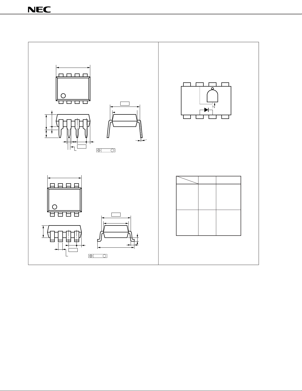
PACKAGE DIMENSIONS (Unit: mm)
PS9601 PIN CONNECTIONS (Top View)
10.16 MAX.
85
3.8
4.55
MAX.
2.8
MIN.
PS9601L
3.8
MAX.
14
MAX.
0.65
1.34
10.16 MAX.
85
14
2.54
0.50 ±0.10
2.54
1.34 ±0.10
1.27
MAX.
0.25
1.27
MAX.
0.25
9.60 ±0.4
M
M
7.62
6.5
7.62
6.5
0 to 15˚
0.05 to 0.2
0.9
±0.25
PIN Function
INPUT 1. NC
2. Anode
3. Cathode
4. NC
OUTPUT 5. GND
6. VO
7. VE*
8. VCC
*VE is pulled-up to
2
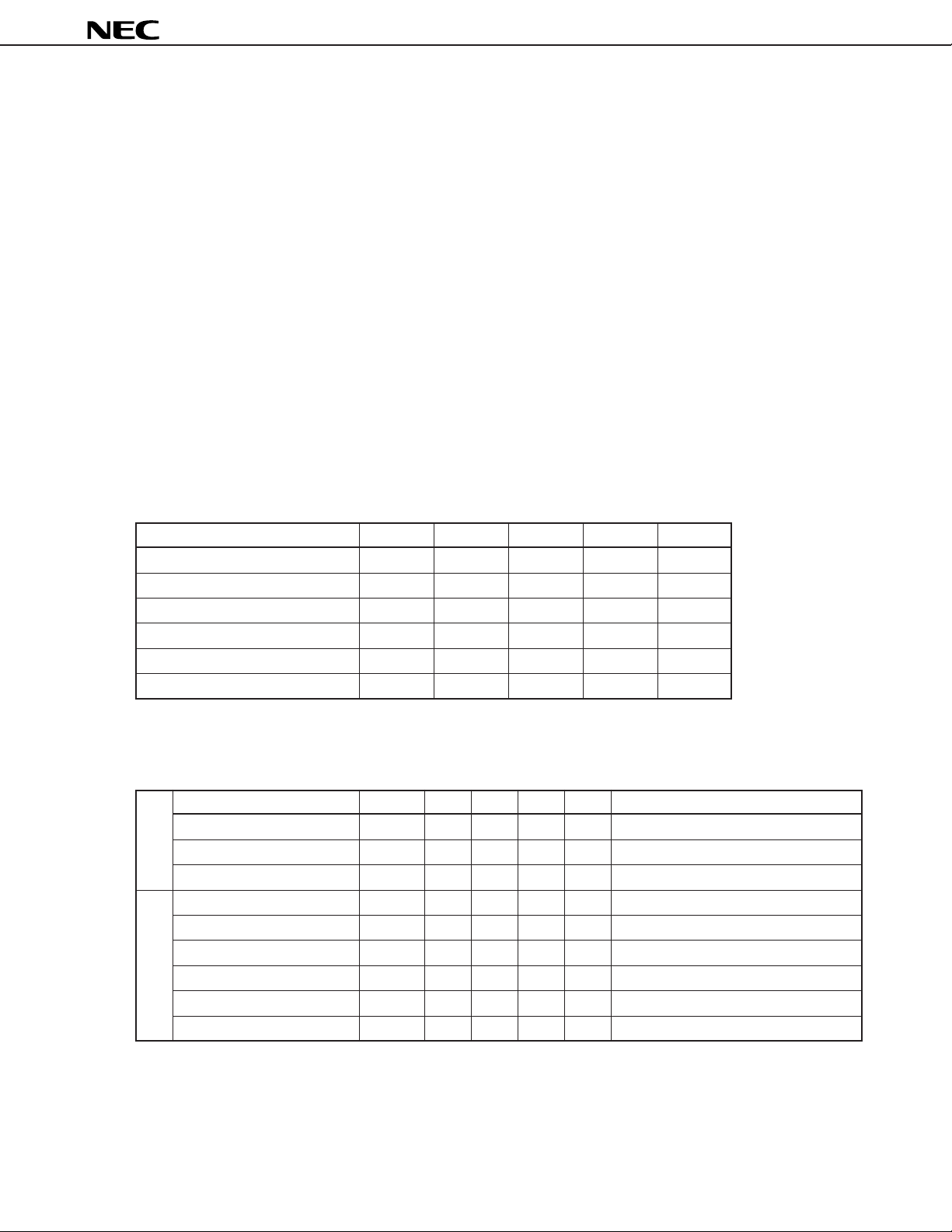
ABSOLUTE MAXIMUM RATINGS (TA = 25 ˚C)
Diode
Forward Current IF 30 mA
Reverse Voltage VR 5V
Power Dissipation P
Detector
Supply Voltage VCC 7V
Output Voltage V
Output Current IO 50 mA
Enable Voltage VE 5.5 V
Power Dissipation P
Isolation Voltage *
1
Operating Temperature Topt –40 to +85 ˚C
Storage Temperature T
*1 AC voltage for 1 minute TA = 25 ˚C, RH = 60 % between input and output.
D 60 mW
O 7V
C 85 mW
BV 5 000 Vr.m.s.
stg –55 to +125 ˚C
PS9601, PS9601L
RECOMMENDED OPERATING CONDITIONS (TA = 25 ˚C)
PARAMETER SYMBOL MIN. TYP. MAX. UNIT
Low Level Input Current IFL 0 250
High Level Input Current IFH 71015mA
High Level Enable Voltage VEH 2VCC V
High Level Enable Voltage VEL 0 0.8 V
Supply Voltage VCC 4.5 5 5.5 V
Operating Temperature Topt 02570˚C
µ
A
* By-pass capacitor of more than 0.1 µF is used between VCC and GND near device.
ELECTRICAL CHARACTERISTICS (TA = –40 to +85 ˚C)
PARAMETER SYMBOL MIN. TYP. MAX. UNIT TEST CONDITIONS
Forward Voltage VF 1.4 1.65 1.9 V IF = 10 mA, TA = 25 ˚C
DiodeDetector
Reverse Current IR 10
Capacitance Ct 60 pF V = 0, f = 1 MHz, TA = 25 ˚C
High Level Output Current IOH 2 250
Low Level Output Voltage VOL 0.2 0.6 V
High Level Supply Current ICCH 5710mAVCC = 5.5 V, VE = 0.5 V, IF = 0
Low Level Supply Current ICCL 10 13 18 mA VCC = 5.5 V, VE = 2 V, IF = 10 mA
High Level Enable Current IEH –0.7 –1 –1.5 mA VCC = 5.5 V, VEH = 2 V
Low Level Enable Current IEL –1 –1.4 –2 mA VCC = 5.5 V, VEL = 0.5 V
µ
AVR = 5 V, TA = 25 ˚C
µ
AVCC = VO = 5.5 V, IF = 250 µs, VE = 2 V
VCC = 5.5 V, IF = 5 mA, VE = 2 V, IO = 13 mA
3
 Loading...