

DATA SHEET
PHOTOCOUPLER
PS2711-1
HIGH CTR
4-PIN SOP PHOTOCOUPLER
DESCRIPTION
The PS2711-1 is an optically coupled isolator containing a GaAs light emitting diode and an NPN silicon
phototransistor in a plastic SOP for high density applications.
The package is an SOP (Small Outline Package) type for high density mounting applications.
FEATURES
• High current transfer ratio (CTR = 200 % TYP. @ IF = 1mA)
• High isolation voltage (BV = 3 750 Vr.m.s.)
• Small and thin package (4-pin SOP)
• Ordering number of tape product: PS2711-1-F3, F4
• UL approved: File No. E72422 (S)
−NEPOCTM Series−
APPLICATIONS
• Programmable logic controllers
• Small power supply
•Hybrid IC
• Modem/FAX
The information in this document is subject to change without notice. Before using this document, please
confirm that this is the latest version.
Not all devices/types available in every country. Please check with local NEC representative for
availability and additional information.
Document No. P14945EJ1V0DS00 (1st edition)
Date Published July 2000 NS CP(K)
Printed in Japan
©
2000
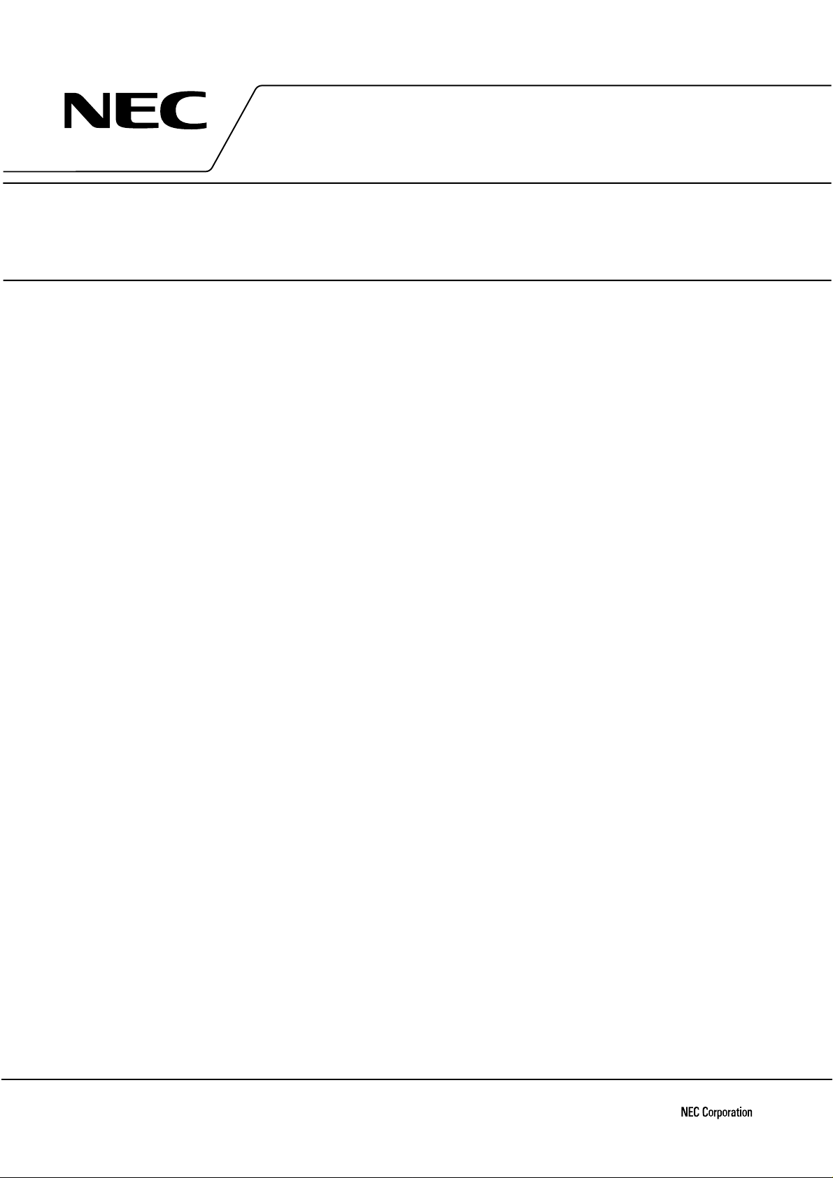
PACKAGE DIMENSIONS
in millimeters
PS2711-1
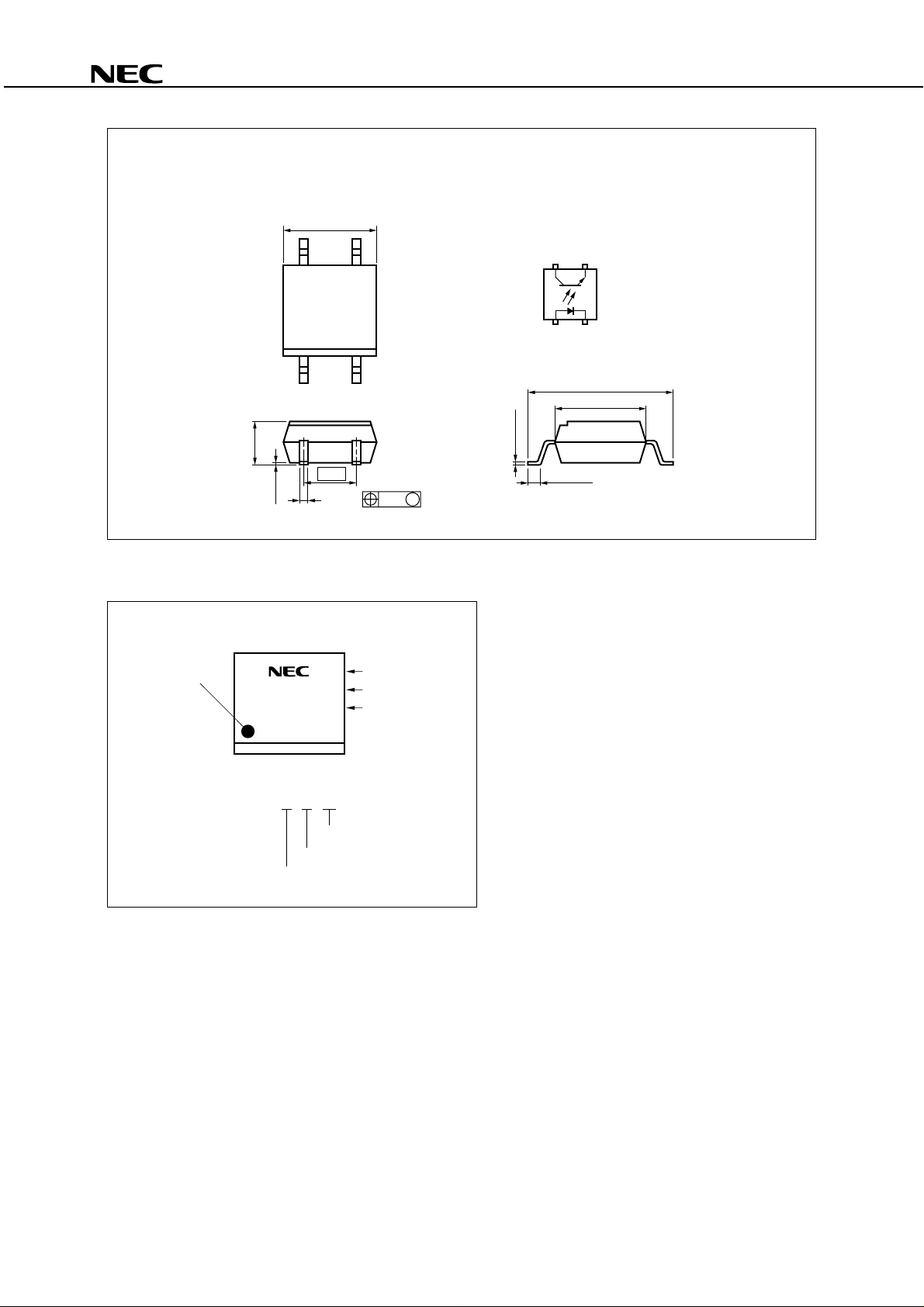
MARKING
No. 1 pin Mark
2.1±0.2
0.1±0.1
2711
N003
4±0.5
2.54
0.4
+0.10
0.25 M
–0.05
Trade Mark
Type Number
Assembly Lot
+0.10
–0.05
0.15
TOP VIEW
43
12
7.0±0.3
4.4
0.5±0.3
1. Anode
2. Cathode
3. Emitter
4. Collector
N003
Week Assembled
Year Assembled
(Last 1 Digit)
CTR Rank Name
2
Data Sheet P14945EJ1V0DS00
ORDERING INFORMATION
PS2711-1
Part Number Package Packing Style
Safety Standards
Approval
Application Part
Number
PS2711-1 4-pin SOP 50 pcs (Tape 50 pcs cut) UL approved PS2711-1
PS2711-1-F3 Embossed Tape 3 500 pcs/reel
PS2711-1-F4
For the application of the Safety Standard, following part number should be used.
*1
ABSOLUTE MAXIMUM RATINGS (TA = 25 °°°°C, unless otherwise specified)
Parameter Symbol Ratings Unit
Diode Forward Current (DC) I
Reverse Voltage V
Power Dissipation Derati ng∆PD/°C0.8mW/
Power Dissipation P
Peak Forward Current
*1
Transistor Collector to Emitter Voltage V
Emitter to Collector Voltage V
Collector Current I
Power Dissipation Derati ng∆PC/°C1.5mW/
Power Dissipation P
Isolation Voltage
*2
Operating Ambient Temperature T
Storage Temperature T
F
R
50 mA
6V
°
I
D
FP
CEO
ECO
C
80 mW
0.5 A
40 V
5V
40 mA
°
C
150 mW
BV 3 750 Vr.m.s.
A
stg
–55 to +100
–55 to +150
°
C
°
C
C
C
*1
PW = 100
*1
AC voltage for 1 minute at TA = 25 °C, RH = 60 % between input and output
*2
µ
s, Duty Cycle = 1 %
Data Sheet P14945EJ1V0DS00
3
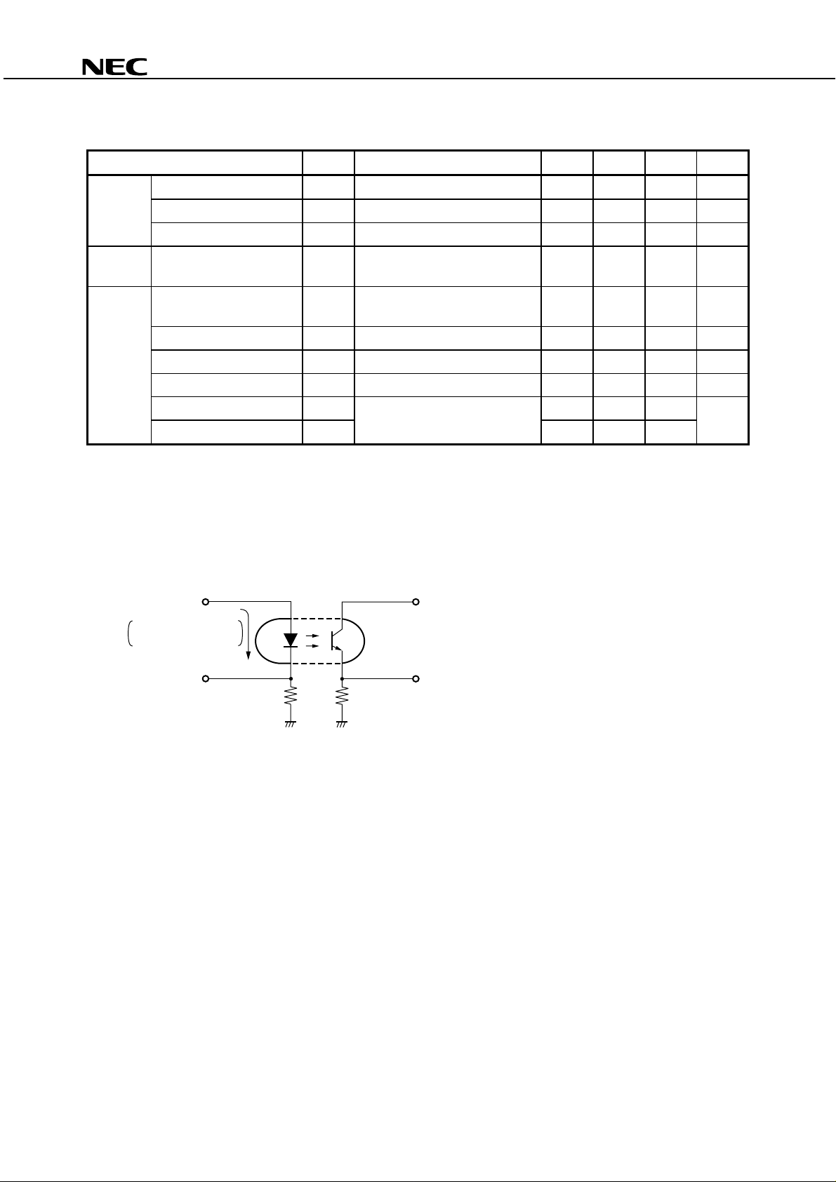
ELECTRICAL CHARACTERISTICS (TA = 25 °°°°C)
Parameter Symbol Conditions MIN. TYP. MAX. Unit
PS2711-1
Diode Forward Voltage V
Reverse Current I
Terminal Capacitance C
Transistor Collector to Emitter Dark
Current
Coupled Current Transf er Rat i o
*1
C/IF
(I
)
CTR IF = 1 mA, VCE = 5 V 100 200 400 %
Collector Saturation Voltage V
Isolation Resistance R
Isolation Capacitance C
*2
*2
CTR rank
*1
Rise Time
Fall Time
N : 100 to 400 (%)
K : 200 to 400 (%)
L : 150 to 300 (%)
M: 100 to 200 (%)
Test circuit for switching time
*2
F
IF = 5 mA 1.15 1.4 V
R
VR = 5 V 5
t
V = 0 V, f = 1 MHz 30 pF
CEOIF
I
CE (sat)IF
t
t
= 0 mA, VCE = 40 V 100 nA
= 1 mA, IC = 0.2 mA 0.3 V
I-O
I-O
V
I-O
V = 0 V, f = 1 MHz 0.4 pF
r
VCC = 5 V, IC = 2 mA, RL = 100
f
= 1 kV
DC
Ω
10
11
4
5
µ
A
Ω
µ
s
Pulse Input
PW = 100 s
µ
Duty cycle = 1/10
In monitor
I
F
50 Ω
RL = 100 Ω
V
CC
V
OUT
4
Data Sheet P14945EJ1V0DS00

TYPICAL CHARACTERISTICS (TA = 25 °°°°C, unless otherwise specified)
PS2711-1
DIODE POWER DISSIPATION vs.
AMBIENT TEMPERATURE
100
80
(mW)
D
60
40
20
Diode Power Dissipation P
0
25
Ambient Temperature TA (˚C)
50
FORWARD CURRENT vs.
FORWARD VOLTAGE
100
10
(mA)
F
A
= +100 ˚C
T
+60 ˚C
+25 ˚C
1
75
100
TRANSISTOR POWER DISSIPATION
vs. AMBIENT TEMPERATURE
200
(mW)
C
150
100
50
Transistor Power Dissipation P
0
25 50 75 100
Ambient Temperature TA (˚C)
COLLECTOR TO EMITTER DARK
CURRENT vs. AMBIENT TEMPERATURE
10 000
(nA)
CEO
1 000
VCE = 40 V
100
20 V
10 V
0.1
Forward Current I
0.01
0.0 0.5 1.0 1.5 2.0
Forward Voltage VF (V)
–25 ˚C
–50 ˚C
COLLECTOR CURRENT vs.
COLLECTOR TO EMITTER VOLTAGE
25
IF = 10 mA
20
(mA)
C
15
10
Collector Current I
5
Collector to Emitter Voltage VCE (V)
5 mA
2 mA
6842010
0 ˚C
0.5 mA
1 mA
10
1
Collector to Emitter Dark Current I
–25
0
Ambient Temperature TA (˚C)
25
50
COLLECTOR CURRENT vs.
COLLECTOR SATURATION VOLTAGE
100
10 mA
5 mA
2 mA
(mA)
C
10
1 mA
1
Collector Current I
0.1
0.0 0.2 0.4 0.6 0.8 1.0
Collector Saturation Voltage V
F
= 0.5mA
I
75
CE(sat)
100
(V)
Data Sheet P14945EJ1V0DS00
5

PS2711-1
NORMALIZED CURRENT TRANSFER
RATIO vs. AMBIENT TEMPERATURE
1.6
1.4
1.2
1.0
0.8
0.6
0.4
Normalized to 1.0
0.2
Normalized Current Transfer Ratio CTR
0.0
–50
–25
025
Ambient Temperature T
A
= 25 ˚C,
at T
I
F
= 1 mA, VCE = 5 V
50 75
A
(˚C)
SWITCHING TIME vs.
LOAD RESISTANCE
100
C
= 2 mA,
I
CC
= 5 V,
V
CTR = 200 %
µ
10
t
f
t
r
t
d
1
Switching Time t ( s)
t
s
100
CURRENT TRANSFER RATIO vs.
FORWARD CURRENT
500
V
CE
= 5 V,
n = 3
400
300
200
100
Current Transfer Ratio CTR (%)
0
0.01
0.1
1
Forward Current IF (mA)
SWITCHING TIME vs.
LOAD RESISTANCE
1 000
I
F
= 1 mA,
V
CC
= 5 V,
CTR = 200 %
100
µ
10
1
Switching Time t ( s)
10
100
t
f
t
s
t
r
t
d
0.1
0
–5
–10
–15
Normalized Gain Gv
–20
–25
0.1
Remark
The graphs indicate nominal characteristics.
10010
1 k
Load Resistance RL (kΩ)
FREQUENCY RESPONSE
RL = 1 kΩ
300 Ω
1
10
Frequency f (kHz)
100 1 000
100 Ω
10 k
0.1
100 1k 10 k 100 k
Load Resistance RL (kΩ)
LONG TERM CTR DEGRADATION
1.2
IF = 1 mA
1.0
0.8
0.6
0.4
CTR (Relative Value)
0.2
0
10
10
2
TA = 25 ˚C
TA = 60 ˚C
3
10
Time (Hr)
10
10
5
4
10
6
6
Data Sheet P14945EJ1V0DS00

TAPING SPECIFICATIONS (in millimeters)
Outline and Dimensions (Tape)
2.0±0.1
4.0±0.1
1.55±0.1
1.75±0.1
PS2711-1
2.4±0.1
1.55±0.1
8.0±0.1
Tape Direction
PS2711-1-F3
Outline and Dimensions (Reel)
4.6±0.1
1
2
0
5.5±0.1
˚
12.0±0.2
PS2711-1-F4
7.4±0.1
0.3
1.5
2.0±0.5
1.5±0.5
6
0
˚
Packing: 3 500 pcs/reel
Data Sheet P14945EJ1V0DS00
21.0±0.8
φ
6.0±1
330
φ
80±5.0
13.0±0.5
φ
φ
12.4
+2.0
–0.0
7

NOTES ON HANDLING
1. Recommended soldering conditions
(1) Infrared reflow soldering
• Peak reflow temperature 235 °C or below (package surface temperature)
• Time of temperature higher than 210 °C 30 seconds or less
• Number of reflows Three
• Flux Rosin flux containing small amount of chlorine (The flux with a
maximum chlorine content of 0.2 Wt % is recommended.)
Recommended Temperature Profile of Infrared Reflow
(heating)
to 10 s
235 ˚C (peak temperature)
210 ˚C
to 30 s
PS2711-1
100 to 160 ˚C
60 to 120 s
(preheating)
Package Surface Temperature T (˚C)
Time (s)
(2) Dip soldering
• Temperature 260 °C or below (molten solder temperature)
• Time 10 seconds or less
• Number of times One (Allowed to be dipped in solder including plastic mold portion.)
• Flux Rosin flux containing small amount of chlorine (The flux with a maximum chlorine content of
0.2 Wt % is recommended.)
(3) Cautions
•Fluxes
Avoid removing the residual flux with freon-based and chlorine-based cleaning solvent.
2. Cautions regarding noise
Be aware that when voltage is applied suddenly between the photocoupler’s input and output or between
corrector-emitters at startup, the output side may enter the on state, even if the voltage is within the absolute
maximum ratings.
8
Data Sheet P14945EJ1V0DS00

[MEMO]
PS2711-1
Data Sheet P14945EJ1V0DS00
9

[MEMO]
PS2711-1
10
Data Sheet P14945EJ1V0DS00

[MEMO]
PS2711-1
Data Sheet P14945EJ1V0DS00
11

PS2711-1
CAUTION
Within this device there exists GaAs (Gallium Arsenide) material which is a
harmful substance if ingested. Please do not under any circumstances break the
hermetic seal.
NEPOC is a trademark of NEC Corporation.
•
The information in this document is current as of July, 2000. The information is subject to change
without notice. For actual design-in, refer to the latest publications of NEC's data sheets or data
books, etc., for the most up-to-date specifications of NEC semiconductor products. Not all products
and/or types are available in every country. Please check with an NEC sales representative for
availability and additional information.
•
No part of this document may be copied or reproduced in any form or by any means without prior
written consent of NEC. NEC assumes no responsibility for any errors that may appear in this document.
•
NEC does not assume any liability for infringement of patents, copyrights or other intellectual property rights of
third parties by or arising from the use of NEC semiconductor products listed in this document or any other
liability arising from the use of such products. No license, express, implied or otherwise, is granted under any
patents, copyrights or other intellectual property rights of NEC or others.
•
Descriptions of circuits, software and other related information in this document are provided for illustrative
purposes in semiconductor product operation and application examples. The incorporation of these
circuits, software and information in the design of customer's equipment shall be done under the full
responsibility of customer. NEC assumes no responsibility for any losses incurred by customers or third
parties arising from the use of these circuits, software and information.
•
While NEC endeavours to enhance the quality, reliability and safety of NEC semiconductor products, customers
agree and acknowledge that the possibility of defects thereof cannot be eliminated entirely. To minimize
risks of damage to property or injury (including death) to persons arising from defects in NEC
semiconductor products, customers must incorporate sufficient safety measures in their design, such as
redundancy, fire-containment, and anti-failure features.
•
NEC semiconductor products are classified into the following three quality grades:
"Standard", "Special" and "Specific". The "Specific" quality grade applies only to semiconductor products
developed based on a customer-designated "quality assurance program" for a specific application. The
recommended applications of a semiconductor product depend on its quality grade, as indicated below.
Customers must check the quality grade of each semiconductor product before using it in a particular
application.
"Standard": Computers, office equipment, communications equipment, test and measurement equipment, audio
and visual equipment, home electronic appliances, machine tools, personal electronic equipment
and industrial robots
"Special": Transportation equipment (automobiles, trains, ships, etc.), traffic control systems, anti-disaster
systems, anti-crime systems, safety equipment and medical equipment (not specifically designed
for life support)
"Specific": Aircraft, aerospace equipment, submersible repeaters, nuclear reactor control systems, life
support systems and medical equipment for life support, etc.
The quality grade of NEC semiconductor products is "Standard" unless otherwise expressly specified in NEC's
data sheets or data books, etc. If customers wish to use NEC semiconductor products in applications not
intended by NEC, they must contact an NEC sales representative in advance to determine NEC's willingness
to support a given application.
(Note)
(1) "NEC" as used in this statement means NEC Corporation and also includes its majority-owned subsidiaries.
(2) "NEC semiconductor products" means any semiconductor product developed or manufactured by or for
NEC (as defined above).
M8E 00. 4
 Loading...