


EP350 BASICO


Technical Information Updates
As we continue to make engineering enhancements to our products, the information in our
Service Manuals need to be updated accordingly. If you wish to be informed of these
updates, kindly fill in and fax us your details.
Manual No.:6878419A01
Kindly complete the Service Manual Feedback Form on the next page to help us ensure
that you receive the most accurate and complete information.
Fax to: 6-04-6194467
The Technical Publications Coordinator,
Global Customer Documentation,
R&D Department,
Motorola Penang.
Your Details
N a m e / C o n t a c t P e r s o n :
Company Name:
Address:
Telephone No.:
Fax No.:
Email Address:
How would you like to receive the update notification?
Through:
mail email fax

Service Manual Feedback Form
We believe that reports from users provide valuable information for producing quality
manuals. Kindly take a few moments to provide feedback on this manual. Thank you for
your cooperation.
1. Please check all the appropriate boxes:
2. How do you rate this particular Service Manual?
excellent very good good fair poor
3. Did this Service manual provide you with the information necessary to service and
maintain the specific equipment?
very much so generally yes to some extent no
4. We would appreciate any corrections or recommendations for improving this manual.
Please include the specific page number(s) of the diagram or procedure in question.
5. General comments/suggestions:
Manual No.:6878419A01
Fax to: 6-04-6194467
The Technical Publications Coordinator,
Global Customer Documentation,
R&D Department,
Motorola Penang.
Complete
Incomplete
Correct
Incorrect
Clear
Confusing
Size
Adequate
Size
Too Small
Not Covered
in this Manual
Disassembly
Procedures
Alignment
Procedures
Exploded
Views
Schematic
Diagrams
Circuit Board
Details
Electrical Parts
List
Exploded View
Parts List

i
COPYRIGHT
Copyrights
© 2009 by Motorola, Inc. All rights reserved.
No part of this manual may be reproduced, transmitted, stored in a retrieval system, or translated into
any language or computer language, in any form or by any means, without the prior written
permission of Motorola Inc.
Computer Software Copyrights
The Motorola products described in this manual may include copyrighted Motorola computer
programs stored in semiconductor memories or other media. Laws in the United States and other
countries preserve for Motorola certain exclusive rights for copyrighted computer programs including,
but not limited to, the exclusive right to copy or reproduce in any form the copyrighted computer
program. Accordingly, any copyrighted Motorola computer programs contained in the Motorola
products described in this manual may not be copied, reproduced, modified, reverse-engineered, or
distributed in any manner without the express written permission of Motorola. Furthermore, the
purchase of Motorola products shall not be deemed to grant either directly or by implication, estoppel,
or otherwise, any license under the copyrights, patents or patent applications of Motorola, except for
the normal non-exclusive royalty-free license to use that arises by operation of law in the sale of a
product.
Trademarks
MOTOROLA and the Stylized M Logo are registered in the U.S.Patent and Trademark Office. All
other product or service names are the property of their respective owners.
ii
SAFETY
Product Safety and RF Exposure Compliance
ATTENTION!
This is restricted to occupational use only to satisfy ICNIRP RF energy exposure
requirements. Before using this product, read the RF energy awareness information and
operating instructions in the Product Safety and RF Exposure booklet enclosed with your
radio (Motorola Publication part number 68007024010) to ensure compliance with RF energy
exposure limits.
For a list of Motorola-approved antennas, and other accessories, visit the following web site
which lists approved accessories: http://www.motorola.com/governmentandenterprise
These servicing instructions are for use by qualified personnel only. To reduce the
risk of electric shock, do not perform any servicing other than that contained in the
Operating Instructions unless you are qualified to do so. Refer all servicing to
qualified service personnel.
Before using this product, read the operating instructions for safe usage contained
in the Product Safety and RF Exposure booklet enclosed with your radio.

iii
DOCUMENT HISTORY
The following major changes have been implemented in this manual since the previous edition:
Edition Description Date
6878419A01-A Initial edition Feb. 2009
6878419A01-B Added UHF1 403 – 447 MHz information Sept. 2009
CHAPTER 1 : Model Charts and Test Specifications
Updated UHF1 range to 403 – 447 MHz
Added UHF1 model chart and specifications
Updated Receiver, Transmitter, PLL Synthesizer, TX Audio
Block Diagrams
CHAPTER 3 : Test Equipment, Service Aids, and Service Tools
Updated “Wiring of the Connectors” diagram
CHAPTER 5 : Radio Programming and Tuning
Updated “CPS Programming Setup” diagram
Updated “Radio Tuning Setup diagram
Added UHF1 band in “Transmitter Alignment Options” table
CHAPTER 6 : Maintenance (FKP)
Added UHF1 PCB parts list
Updated Exploded View (Remove Tanapa Label)
Updated Quantity in Parts List
CHAPTER 7: Maintenance (LKP)
Added UHF1 PCB parts list
Updated Exploded View (Remove Tanapa Label)
Updated Quantity in Parts List

iv
Notes

Table of Contents v
Table of Contents
Copyright ........................................................................................................ i
Safety ............................................................................................................. ii
Document History ........................................................................................ iii
Chapter 1 Model Charts and Test Specifications .............................. 1-1
1.1 Radio Model Information................................................................................................................ 1-1
1.2 Model Chart for UHF2, 435–480 MHz ........................................................................................... 1-2
1.3 Model Chart for VHF, 136–174 MHz .............................................................................................1-3
1.4 Model Chart for UHF1, 403–447 MHz ........................................................................................... 1-4
1.5 UHF2 Specifications ...................................................................................................................... 1-5
1.6 VHF Specifications ........................................................................................................................ 1-6
1.7 UHF1 Specifications ...................................................................................................................... 1-7
Chapter 2 Theory Of Operation ........................................................... 2-1
2.1 Introduction .................................................................................................................................... 2-1
2.2 Major Assemblies .......................................................................................................................... 2-1
2.2.1 Receiver............................................................................................................................ 2-1
2.2.1.1 RX Front End..................................................................................................... 2-2
2.2.1.2 RX Back End ..................................................................................................... 2-2
2.2.1.3 RX Squelch........................................................................................................ 2-3
2.2.2 Transmitter........................................................................................................................ 2-4
2.2.3 Phase Lock Loop Synthesizer .......................................................................................... 2-5
2.2.4 RX Audio Circuit ............................................................................................................... 2-6
2.2.5 TX Audio Circuit................................................................................................................ 2-7
2.2.6 Microcontroller .................................................................................................................. 2-8
2.2.7 Power Supply.................................................................................................................... 2-8
Chapter 3 Test Equipment, Service Aids, and Service Tools........... 3-1
3.1 Test Equipment.............................................................................................................................. 3-1
3.2 Service Aids................................................................................................................................... 3-2
Chapter 4 Performance Checks .......................................................... 4-1
4.1 General .......................................................................................................................................... 4-1
4.2 Power–Up Self Test....................................................................................................................... 4-1
4.3 LCD/LED/Button/Volume Knob Test Mode.................................................................................... 4-1
Chapter 5 Radio Programming and Tuning ....................................... 5-1
5.1 Introduction .................................................................................................................................... 5-1
5.2 CPS Programming Setup .............................................................................................................. 5-1
5.3 Radio-to-Radio Cloning ................................................................................................................. 5-1

vi Table of Contents
5.4 Radio Tuning Setup ....................................................................................................................... 5-2
5.4.1 Initial Test Equipment Control Settings............................................................................. 5-3
5.5 Transmitter Alignment Options ......................................................................................................5-3
5.5.1 Transmit High Power Tuning ............................................................................................ 5-3
5.5.2 Transmit Low Power Tuning ............................................................................................. 5-4
5.5.3 Transmit Modulation Tuning .............................................................................................5-5
5.5.3.1 Service Monitor Setting...................................................................................... 5-5
5.5.3.2 Transmit 12.5 kHz Modulation Tuning ...............................................................5-6
5.5.3.3 Transmit 25 kHz Modulation Tuning ..................................................................5-7
5.6 Receiver Tuning............................................................................................................................. 5-8
5.6.1 Service Monitor Setting..................................................................................................... 5-8
5.6.2 Receive 12.5 kHz-Band Normal Squelch Tuning.............................................................. 5-9
5.6.3 Receive 12.5 kHz-Band Tight Squelch Tuning ............................................................... 5-10
5.6.4 Receive 25 kHz-Band Normal Squelch Tuning............................................................... 5-11
5.6.5 Receive 25 kHz-Band Tight Squelch Tuning .................................................................. 5-12
5.7 Utilities ......................................................................................................................................... 5-13
5.7.1 Program Serial No. .........................................................................................................5-13
5.8 Front Panel Programming............................................................................................................ 5-14
5.8.1 Introduction ..................................................................................................................... 5-14
5.8.2 Dealer and User Configurations...................................................................................... 5-14
5.8.2.1 Switching between Dealer and User Configurations........................................ 5-14
5.8.3 Entering Programming Mode .......................................................................................... 5-15
5.8.4 Exiting Programming Mode............................................................................................. 5-15
5.8.5 Accessing Front Panel Programming Mode Parameters................................................ 5-15
5.8.6 Editing Front Panel Programming Mode Parameters ..................................................... 5-16
5.8.7 Factory Reset..................................................................................................................5-23
Chapter 6 Maintenance – EP350 (Full Keypad Model) ..................... 6-1
6.1 Introduction .................................................................................................................................... 6-1
6.2 Preventive Maintenance ................................................................................................................ 6-1
6.2.1 Inspection..........................................................................................................................6-1
6.2.2 Cleaning Procedures ........................................................................................................6-1
6.3 Safe Handling of CMOS and LDMOS Devices .............................................................................. 6-2
6.4 Repair Procedures and Techniques – General.............................................................................. 6-3
6.5 Disassembling and Reassembling the Radio ................................................................................ 6-6
6.5.1 Radio Disassembly – Detailed .......................................................................................... 6-7
6.5.1.1 Front Housing From Chassis Disassembly........................................................ 6-7
6.5.1.2 Chassis Assembly Disassembly ...................................................................... 6-10
6.5.1.3 Front Circuit Board, Display Module and Keypad Disassembly.......................6-11
6.5.1.4 Speaker Disassembly ...................................................................................... 6-12
6.5.2 Radio Reassembly – Detailed......................................................................................... 6-13
6.5.2.1 Speaker Reassembly....................................................................................... 6-13
6.5.2.2 Front Circuit Board, Display Module and Keypad Reassembly ....................... 6-14
6.5.2.3 Chassis Assembly Reassembly....................................................................... 6-15
6.5.2.4 Chassis and Front Housing Reassembly......................................................... 6-17
6.6 Torque List ................................................................................................................................... 6-17
6.7 Mechanical View and Parts List ................................................................................................... 6-18
6.7.1 EP350 (Full Keypad without Channel Knob) Exploded View and Parts List................... 6-18
Chapter 7 Maintenance – EP350 (Limited Keypad Model)............... 7-1
7.1 Introduction .................................................................................................................................... 7-1

Table of Contents vii
7.2 Preventive Maintenance ................................................................................................................ 7-1
7.2.1 Inspection ......................................................................................................................... 7-1
7.2.2 Cleaning Procedures ........................................................................................................7-1
7.3 Safe Handling of CMOS and LDMOS Devices.............................................................................. 7-2
7.4 Repair Procedures and Techniques – General ............................................................................. 7-3
7.5 Disassembling and Reassembling the Radio ................................................................................ 7-6
7.5.1 Radio Disassembly – Detailed.......................................................................................... 7-7
7.5.1.1 Front Housing From Chassis Disassembly........................................................ 7-7
7.5.1.2 Chassis Assembly Disassembly ...................................................................... 7-10
7.5.1.3 Front Circuit Board, Display Module and Keypad Disassembly ...................... 7-12
7.5.1.4 Speaker Disassembly...................................................................................... 7-13
7.5.2 Radio Reassembly – Detailed ........................................................................................ 7-13
7.5.2.1 Speaker Reassembly....................................................................................... 7-13
7.5.2.2 Front Circuit Board, Display Module and Keypad Reassembly....................... 7-14
7.5.2.3 Chassis Assembly Reassembly....................................................................... 7-15
7.5.2.4 Chassis and Front Housing Reassembly......................................................... 7-17
7.6 Torque List................................................................................................................................... 7-18
7.7 Mechanical View and Parts List................................................................................................... 7-18
7.7.1 EP350 (Limited Keypad without Channel Knob) Exploded View and Parts List ............. 7-18
Chapter 8 Troubleshooting Tables ..................................................... 8-1
8.1 Error Codes ................................................................................................................................... 8-1
8.2 Troubleshooting Table for Receiver............................................................................................... 8-2
8.3 Troubleshooting Table for Transmitter........................................................................................... 8-3
Appendix A Accessories.........................................................................A-1
Appendix B Warranty, Service Support, and Replacement Parts .......B-1
B.1 Scope of Manual ............................................................................................................................B-1
B.2 Warranty ........................................................................................................................................B-1
B.2.1 What This Warranty Covers And For How Long...............................................................B-1
B.2.2 General Provisions ...........................................................................................................B-1
B.2.3 How To Get Warranty Service ..........................................................................................B-2
B.2.4 What This Warranty Does Not Cover ...............................................................................B-2
B.2.5 Patent And Software Provisions .......................................................................................B-3
B.2.6 Piece Parts .......................................................................................................................B-4
B.2.6.1 Basic Ordering................................................................................................... B-4
B.2.6.2 Motorola Online .................................................................................................B-4
B.2.7 Motorola Service Centers .................................................................................................B-4
Glossary of Terms .....................................................................................G-1

viii List of Figures
List of Figures
Figure 2-1. Receiver Block Diagram ...................................................................................................2-1
Figure 2-2. Transmitter Block Diagram ...............................................................................................2-4
Figure 2-3. PLL Synthesizer Block Diagram....................................................................................... 2-5
Figure 2-4. RX Audio Block Diagram..................................................................................................2-6
Figure 2-5. TX Audio Block Diagram ..................................................................................................2-7
Figure 3-1. Programming/Test Cable (PMDN4077_R)....................................................................... 3-3
Figure 3-2. Cloning Cable (PMDN4076_R) ........................................................................................ 3-3
Figure 3-3. Wiring of the Connectors .................................................................................................. 3-3
Figure 4-4. LCD Indication.................................................................................................................. 4-1
Figure 5-5. CPS Programming Setup ................................................................................................. 5-1
Figure 5-6. Radio Tuning Setup.......................................................................................................... 5-2
Figure 5-7. Tx High Power Window (High Power) .............................................................................. 5-4
Figure 5-8. Tx Low Power Window (Low Power)................................................................................ 5-5
Figure 5-9. Tx Modulation 12.5 kHz Window ...................................................................................... 5-7
Figure 5-10. Tx Modulation 25 kHz Window .........................................................................................5-8
Figure 5-11. Rx 12.5 kHz-band Normal Squelch Tuning Window ...................................................... 5-10
Figure 5-12. Rx 12.5 kHz-band Tight Squelch Tuning Window .......................................................... 5-11
Figure 5-13. Rx 25 kHz-band Normal Squelch Tuning Window ......................................................... 5-12
Figure 5-14. Rx 25 kHz-band Tight Squelch Tuning Window .............................................................5-13
Figure 5-15. Program Radio Serial No. Window................................................................................. 5-13
Figure 6-16. Full Keypad Without Channel Knob Model....................................................................... 6-6
Figure 6-17. Battery and Antenna Removal.......................................................................................... 6-7
Figure 6-18. Knob Removal.................................................................................................................. 6-7
Figure 6-19. Chassis Removal.............................................................................................................. 6-8
Figure 6-20. Speaker Wire and Flexible Cable Connection.................................................................. 6-8
Figure 6-21. Speaker Wire Removal..................................................................................................... 6-9
Figure 6-22. Unlatch the Flexible Cable................................................................................................ 6-9
Figure 6-23. Sub-Circuit Board and Accessory Bracket Removal ...................................................... 6-10
Figure 6-24. Main Circuit Board, finger strips, O-ring and Battery Contact Seal Removal(UHF2) .....6-11
Figure 6-25. Main Circuit Board, finger strips, O-ring and Battery Contact Seal Removal(UHF1) .....6-11
Figure 6-26. Front Circuit Board Removal .......................................................................................... 6-12
Figure 6-27. LCD and Keypad Removal ............................................................................................. 6-12
Figure 6-28. Speaker Removal...........................................................................................................6-13
Figure 6-29. Speaker Reassembly ..................................................................................................... 6-13
Figure 6-30. LCD and Keypad Reassembly .......................................................................................6-14
Figure 6-31. Front Circuit Board Reassembly..................................................................................... 6-14
Figure 6-32. Main Circuit Board, finger strips, O-ring and Battery Contact Seal Reassembly(UHF2) 6-15
Figure 6-34. Sub Circuit Board and Accessory Bracket Reassembly................................................. 6-16
Figure 6-33. Main Circuit Board, finger strips, O-ring and Battery Contact Seal Reassembly(UHF1) 6-16
Figure 6-35. Chassis Assembly and Front Housing Assembly Reassembly ......................................6-17
Figure 6-36. EP350 (Full Keypad without Channel Knob)Radio Exploded View ................................6-18
Figure 7-37. Limited Keypad Without Channel Knob Model ................................................................. 7-6
Figure 7-38. Battery and Antenna Removal.......................................................................................... 7-7
Figure 7-39. Knob Removal.................................................................................................................. 7-8
Figure 7-40. Chassis Removal.............................................................................................................. 7-8
Figure 7-41. Speaker Wire and Flexible Cable Connection.................................................................. 7-9
Figure 7-42. Speaker Wire Removal..................................................................................................... 7-9
Figure 7-43. Unlatch the Flexible Cable.............................................................................................. 7-10
Figure 7-44. Sub-Circuit Board and Accessory Bracket Removal ...................................................... 7-10
Figure 7-45. Main Circuit Board, finger strips, O-ring and Battery Contact Seal Removal(UHF2) .....7-11

List of Figures ix
Figure 7-46. Main Circuit Board, finger strips, O-ring and Battery Contact Seal Removal (UHF1) .... 7-11
Figure 7-47. Front Circuit Board Removal .......................................................................................... 7-12
Figure 7-48. LCD and Keypad Removal............................................................................................. 7-12
Figure 7-49. Speaker Removal........................................................................................................... 7-13
Figure 7-50. Speaker Reassembly ..................................................................................................... 7-14
Figure 7-51. LCD and Keypad Reassembly ....................................................................................... 7-14
Figure 7-52. Front Circuit Board Reassembly .................................................................................... 7-15
Figure 7-53. Main Circuit Board, O-ring and Battery Contact Seal Reassembly(UHF2) .................... 7-16
Figure 7-54. Main Circuit Board, finger strips, O-ring and Battery Contact Seal Reassembly(UHF1) 7-16
Figure 7-55. Sub Circuit Board and Accessory Bracket Reassembly................................................. 7-17
Figure 7-56. Chassis Assembly and Front Housing Assembly Reassembly ...................................... 7-17
Figure 7-57. EP350 (Limited Keypad without Channel Knob) – Exploded View ................................ 7-18

x List of Tables
List of Tables
Table 1-1. Radio Model Number (Example:MDH03RDH8AA7) ........................................................ 1-1
Table 3-2. Recommended Test Equipment ....................................................................................... 3-1
Table 3-3. Service Aids......................................................................................................................3-2
Table 4-4. Radio Operation in Test Mode..........................................................................................4-1
Table 5-5. Initial Equipment Control Settings ....................................................................................5-3
Table 5-6. Transmit High/Low Power Level....................................................................................... 5-3
Table 5-7. Transmit Modulation Tuning .............................................................................................5-5
Table 5-8. Receiver Squelch Tuning ................................................................................................. 5-8
Table 5-9. Front Panel Programming Mode Parameters................................................................. 5-16
Table 6-10. Lead Free Solder Wire Part Number List ......................................................................... 6-3
Table 6-11. Lead Free Solder Paste Part Number List........................................................................6-3
Table 6-12. Torque Chart .................................................................................................................. 6-17
Table 6-13. Parts List (Full Keypad without Channel Knob) .............................................................. 6-19
Table 7-14. Lead Free Solder Wire Part Number List ......................................................................... 7-4
Table 7-15. Lead Free Solder Paste Part Number List........................................................................7-4
Table 7-16. Torque Chart .................................................................................................................. 7-18
Table 7-17. Parts List (Limited Keypad without Channel Knob) ........................................................7-19
Table 8-18. Error Code Display ........................................................................................................... 8-1
Table 8-19. Receiver Troubleshooting Table.......................................................................................8-2
Table 8-20. Transmitter Troubleshooting Table................................................................................... 8-3
Table B-1. Portable Radios and Product Accessories Warranty........................................................B-1
Related Publications
LACR
EP350 Series Radios User Guide
(English, Latin American Spanish, Brazilian Portuguese)...............................................6878081A01
EP350 Series Radios Quick Reference Card
(English, Latin American Spanish, Brazilian Portuguese)............................................. 68007024010
EP350 Basic Service Manual .................................................................................................. 6878419A01
EP350 Detailed Service Manual ..............................................................................................6878422A01
Product Safety and RF Exposure Booklet ................................................................................6881095C98

Notations Used in This Manual xi
Notations Used in This Manual
Throughout the text in this publication, you will notice the use of the following notations. These notations
are used to emphasize that safety hazards exist, and due care must be taken and observed.
Note
An operational procedure, practice, or condition that isessential to emphasize.
CAUTION indicates a potentially hazardous situation which, if not avoided,
might result in equipment damage.

xii Summary of Bands Available
Summary of Bands Available
Table below lists all the bands available in this manual. For details, please refer to the Model Charts section.
Frequency Band Bandwidth Power Level
UHF2 435–480 MHz 1W or 4W
VHF 136– 74 MHz 1W or 5W
UHF1 403–447 MHz 1W or 4W

Chapter 1 Model Charts and Test Specifications
1.1 Radio Model Information
The model number and serial number are located on a label attached to the back of your radio. You
can determine the RF output power, frequency band, protocols, and physical packages. The example
below shows one portable radio model number and its specific characteristics.
Table 1-1. Radio Model Number (Example:MDH03RDH8AA7)
Regional
Prefix
Type o f
Unit
Model
Series
Freq. Band
Power
Level
Physical
Packages
Channel
Spacing
Protocol
Feature
Level
LA H 03 R
UHF
(435–480 MHz)
K
VHF
(136–174 MHz)
M
200MHz
(216–223 MHz)
N
200MHz
(245–247 MHz)
E
300MHz
(350–390 MHz)
Q
UHF
(403–447 MHz)
S
UHF
(470–512 MHz)
D
4 W
C
2 W
E
5 W
H
Limited
Keypad
without
Channel
Knob
K
Full Keypad
without
Channel
Knob
T
Full Keypad
RTTE Model
U
Limited
Keypad
RTTE Model
8
12.5/25k
4
12.5k
6
20/25k
9
12.5/20/
25k
AA 7
No
Front Panel
Prog.
with
Scrambling
1
Fixed Freq.
Tier 1
2
Fixed Freq.
Tier 2
3
Fixed Freq.
Tier 3
4
Fixed Freq.
Tier 4
5
Fixed Freq.
Tier 5
9
Front Panel
Prog.
with
Scrambling
LA = LACR
H = Portable
03 = CP Family Model Series
AA = Conventional
1-2 Model Charts and Test Specifications: Model Chart for UHF2, 435–480 MHz
1.2 Model Chart for UHF2, 435–480 MHz
EP350, UHF2, 435–480 MHz
Model Description
LAH03RDK8AA9AN EP350 435 – 480M 4W 12.5/25K 99C Full Keypad
LAH03RDH8AA7AN EP350 435 – 480M 4W 12.5/25K 99C Limited Keypad
Item Description
X PMUE3148_ 435 – 480M 4W 12.5/25K 99C FKPFPP SCR
X PMUE3144_ 435 – 480M 4W 12.5/25K 99C LKP SCR
X PMDE4010_R 435 – 480M 4W PCB – PMUE3148_AL
X PMDE4012_R 435 – 480M 4W PCB – PMUE3144_AL
X PMDN4130_R Front Circuit Board, FKP
X PMDN4131_R Front Circuit Board, LKP
X X PMDN4129_R Sub Circuit Board, w/o Channel
X X 6878419A01 EP350 BASIC SERVICE MANUAL
X X 6878422A01 EP350 DETAILED SERVICE MANUAL
X = Indicates compatibility with model(s)
Model Charts and Test Specifications: Model Chart for VHF, 136–174 MHz 1-3
1.3 Model Chart for VHF, 136–174 MHz
EP350, VHF, 136–174 MHz
Model Description
LAH03KEK8AA9AN EP350 136 – 174M 5W 12.5/25K 99C Full Keypad
LAH03KEH8AA7AN EP350 136 – 174M 5W 12.5/25K 99C Limited Keypad
Item Description
X PMUD2437_ 136 – 174M 5W 12.5/25K 99CH FKPFPP SCR
X PMUD2441_ 136 – 174M 5W 12.5/25K 99CH LKP SCR
X PMDD4011_R 136 – 174M 5W PCB – PMUD2437_AL
X PMDD4017_R 136 – 174M 5W PCB – PMUD2441_AL
X PMDN4130_R Front Circuit Board, FKP
X PMDN4131_R Front Circuit Board, LKP
X X PMDN4129_R Sub Circuit Board, w/o Channel
X X 6878419A01 EP350 BASIC SERVICE MANUAL
X X 6878422A01 EP350 DETAILED SERVICE MANUAL
X = Indicates compatibility with model(s)

1-4 Model Charts and Test Specifications: Model Chart for UHF1, 403–447 MHz
1.4 Model Chart for UHF1, 403–447 MHz
EP350, UHF1, 403–447 MHz
Model Description
LAH03QDK8AA9AN EP350 403 – 447M 4W 12.5/25K 99C Full Keypad
LAH03QDH8AA7AN EP350 403 – 447M 4W 12.5/25K 99C Limited Keypad
Item Description
PMUE3320_ 403 – 447M 4W 12.5/25K 99C FKPFPP
PMUE3323_ 403 – 447M 4W 12.5/25K 99C LKP
PMDE4028_R 403 – 447M 4W PCB – PMUE3320_AL
PMDE4034_R 403 – 447M 4W PCB – PMUE3323_AL
PMDN4130_R Front Circuit Board, FKP
PMDN4131_R Front Circuit Board, LKP
PMDN4129_R Sub Circuit Board, w/o Channel
6878419A01 EP350 BASIC SERVICE MANUAL
6878422A01 EP350 DETAILED SERVICE MANUAL
X = Indicates compatibility with model(s)
Model Charts and Test Specifications: UHF2 Specifications 1-5
1.5 UHF2 Specifications
General
Self-Quieter Frequencies
Transmitter
Receiver
All specifications are subject to change without notice.
UHF2
Frequency: 435 – 480 MHz
Channel Capacity: 99 Channels
Power Supply: 7.5 Volts ±20%
Dimensions:
(H x W x D)
with
High Capacity Li-Ion
NiMH Std
Li-Ion Std
Batteries:
120 mm x 55 mm x 40.7 mm
120 mm x 55 mm x 36.5 mm
120 mm x 55 mm x 35.5 mm
Weight:
Battery:
High Capacity Li-Ion
NiMH Std
Li-Ion Std
342.0g
394.5g
335.0g
Average Battery Life
@ (5-5-90 Duty
Cycle):
High Capacity Li-Ion
NiMH Std
Li-Ion Std
Capacity
(mAh)
2150
1300
1500
4 W
12 Hrs.
8 Hrs.
8 Hrs.
1 W
14 Hrs.
10 Hrs.
10 Hrs.
UHF2
446.440
446.445
455.895
456.010
456.015
456.125
458.195
460.000
467.785
467.900
468.010
468.125
468.240
470.000
479.900
UHF2
RF Output
NiMH @ 7.5 V:
Low
1 W
High
4 W
Frequency: 435 – 480 MHz
Channel Spacing: 12.5/25 kHz
Freq. Stability:
(-30°C to +60°C)
0.00025%
Spurs/Harmonics: -36 dBm < 1 GHz
-30 dBm > 1 GHz
Audio Response:
(from 6 dB/oct.
Pre-emphasis, 300 to
3000 Hz)
+1, -3 dB
Audio Distortion:
@ 1000 Hz, 60%
Rated Max. Dev.
<5%
FM Noise: <-40 dB
UHF2
12.5 kHz
UHF2
25kHz
Frequency: 435 – 480 MHz
Sensitivity
12 dB EIA SINAD:
0.25 μV (typical)
Adjacent Channel
Selectivity:
-65 dB -70 dB
Intermodulation: -70 dB
Freq. Stability
(-30°C to +60°C):
0.00025%
Spur Rejection: -70 dB
Image and 1/2 I-F
Rejection:
-70 dB
Audio Output
@ <5% Distortion:
500 mW

1-6 Model Charts and Test Specifications: VHF Specifications
1.6 VHF Specifications
General
Self-Quieter Frequencies
Transmitter
Receiver
All specifications are subject to change without notice.\
VHF
Frequency: 136 – 174 MHz
Channel Capacity: 99 Channels
Power Supply: 7.5 Volts ±20%
Dimensions:
(H x W x D)
with
High Capacity Li-Ion
NiMH Std
Li-Ion Std
Batteries:
120 mm x 55 mm x 40.7 mm
120 mm x 55 mm x 36.5 mm
120 mm x 55 mm x 35.5 mm
Weight:
Battery:
High Capacity Li-Ion
NiMH Std
Li-Ion Std
342.0g
394.5g
335.0g
Average Battery Life
@ (5-5-90 Duty
Cycle):
High Capacity Li-Ion
NiMH Std
Li-Ion Std
Capacity
(mAh)
2150
1300
1500
5 W
12 Hrs.
8 Hrs.
8 Hrs.
1 W
14 Hrs.
10 Hrs.
10 Hrs.
VHF
140.000
155.010
155.020
155.030
155.015
155.170
155.180
155.175
155.505
159.995
160.000
160.005
161.450
167.025
167.030
169.995
170.000
170.005
173.985
173.990
VHF
RF Output
NiMH @ 7.5 V:
Low
1 W
High
5 W
Frequency: 136 – 174 MHz
Channel Spacing: 12.5/25 kHz
Freq. Stability:
(-30°C to +60°C)
0.00025%
Spurs/Harmonics: -36 dBm < 1 GHz
-30 dBm > 1 GHz
Audio Response:
(from 6 dB/oct.
Pre-emphasis, 300 to
3000 Hz)
+1, -3 dB
Audio Distortion:
@ 1000 Hz, 60%
Rated Max. Dev.
<5%
FM Noise: <-40 dB
VHF
12.5 kHz
VHF
25kHz
Frequency: 136 – 174 MHz
Sensitivity
12 dB EIA SINAD:
0.25 μV (typical)
Adjacent Channel
Selectivity:
-65 dB -70 dB
Intermodulation: -70 dB
Freq. Stability
(-30°C to +60°C):
0.00025%
Spur Rejection: -70 dB
Image and 1/2 I-F
Rejection:
-70 dB
Audio Output
@ <5% Distortion:
500 mW
Model Charts and Test Specifications: UHF1 Specifications 1-7
1.7 UHF1 Specifications
General
Self-Quieter Frequencies
Transmitter
Receiver
All specifications are subject to change without notice.
UHF1
Frequency: 403 – 447 MHz
Channel Capacity: 99 Channels
Power Supply: 7.5 Volts ±20%
Dimensions:
(H x W x D)
with
High Capacity Li-Ion
NiMH Std
Li-Ion Std
Batteries:
120 mm x 55 mm x 40.7 mm
120 mm x 55 mm x 36.5 mm
120 mm x 55 mm x 35.5 mm
Weight:
Battery:
High Capacity Li-Ion
NiMH Std
Li-Ion Std
342.0g
394.5g
335.0g
Average Battery Life
@ (5-5-90 Duty
Cycle):
High Capacity Li-Ion
NiMH Std
Li-Ion Std
Capacity
(mAh)
2150
1300
1500
4 W
12 Hrs.
8 Hrs.
8 Hrs.
1 W
14 Hrs.
10 Hrs.
10 Hrs.
UHF1
424.355
424.810
442.360
442.365
442.370
444.010
444.015
443.900
444.125
446.030
446.035
446.445
446.450
446.455
446.460
446.675
446.680
UHF1
RF Output
NiMH @ 7.5 V:
Low
1 W
High
4 W
Frequency: 403 – 447 MHz
Channel Spacing: 12.5/25 kHz
Freq. Stability:
(-30°C to +60°C)
0.00025%
Spurs/Harmonics: -36 dBm < 1 GHz
-30 dBm > 1 GHz
Audio Response:
(from 6 dB/oct.
Pre-emphasis, 300 to
3000 Hz)
+1, -3 dB
Audio Distortion:
@ 1000 Hz, 60%
Rated Max. Dev.
<5%
FM Noise: <-40 dB
UHF1
12.5 kHz
UHF1
25 kHz
Frequency: 403 – 447 MHz
Sensitivity
12 dB EIA SINAD:
0.25 μV (typical)
Adjacent Channel
Selectivity:
-65 dB -70 dB
Intermodulation: -70 dB
Freq. Stability
(-30°C to +60°C):
0.00025%
Spur Rejection: -70 dB
Image and 1/2 I-F
Rejection:
-70 dB
Audio Output
@ <5% Distortion:
500 mW

1-8 Model Charts and Test Specifications: UHF1 Specifications
Notes
Chapter 2 Theory Of Operation
2.1 Introduction
This chapter provides a basic theory of operation for the radio components.
2.2 Major Assemblies
• Main PCB – Contains the RF circuits which comprises receiver, transmitter, phase-locked loop
(PLL) frequency synthesizer, micro controller, power supply, audio and digital circuits
• Display and Keypad PCB (Limited and Full Keypad models only) – 8 characters (14 segments
star burst) and 10 icons with backlighting, liquid-crystal display (LCD)
• Volume Knob PCB (PMDN4129AR) – Rotary Volume Knob
2.2.1 Receiver
The radio's receiver is a double conversion super heterodyne with 1st IF of 45.1 MHz and 2nd IF of
455 kHz.
UHF1 receiver design covers the frequency range of 403 – 447 MHz.
UHF2 receiver design covers the frequency range of 435 – 480 MHz.
VHF receiver design covers the frequency range of 136 – 174 MHz.
Figure 2-1. Receiver Block Diagram
Crystal
Filter
Crystal
44.645MHz
1st Mixer
RF
Amp
Preselector
Filter
Postselector
Filter
RX from
A
ntenna Switch
Inj Filter
First LO
from Synthesizer
IF
Amp
IF
Amp
LPF
Ceramic
Filter
Descriminator
455FW
455HW
Quadrature
Detector
RSSI
N/S_SW
Recovered Audio
455C24

2-2 Theory Of Operation: Major Assemblies
2.2.1.1 RX Front End
UHF1 : Receiver Front-end consists of a low pass filter, a pre-selector filter, a low noise RF Amplifier
and a Post-selector filter. Incoming RF signal from the antenna is applied through the Harmonics
Low Pass Filter (L409, L410, L411, C426, C427, C428, C429, C445, C446) and passes through the
transmit/receive switch (CR301) and a varactor-tuned 2-pole pre-selector filter (L320, L324, C351,
C361, CR314 and CR307) before routed to an RF amplifier (Q301). The pre-selector filter is an
8 step Band-shift filter, and the frequency shifting is controlled by varactor diodes (CR314 and
CR307) connected to the CPU. The filter output is coupled to a 13 dB RF amplifier Q301 which
outputs the RF signal to the post-selector filter (L323, L328, C379, and C355) which is also a band
shift filter configured to provide steeper low-side attenuation. The 2 varactor diodes (CR313 and
CR305) with 8 frequency steps are also controlled by the CPU.
UHF
2 : Receiver Front-end consists of a low pass filter, a pre-selector filter, a low noise RF Amplifier
and a Post-selector filter. Incoming RF signal from the antenna is applied through the Harmonics
Low Pass Filter (L409, L410, L411, C426, C427, C428, C429, C445, C446) and passes through the
transmit/receive switch (CR301) and a varactor-tuned 2-pole pre-selector filter (L320, L324, C351,
C361, CR314 and CR307) before routed to an RF amplifier (Q301). The pre-selector filter is an 8
step Band-shift filter, and the frequency shifting is controlled by varactor diodes (CR314 and CR307)
connected to the CPU. The filter output is coupled to a 13 dB RF amplifier Q301 which outputs the
RF signal to the post-selector filter (L323, L322, L328, C379, C354 and C355) which is also a band
shift filter configured to provide steeper low-side attenuation. The 3 varactor diodes (CR313, CR304
and CR305) with 8 frequency steps are also controlled by the CPU.
VHF
: Receiver Front-end consists of a low pass filter, a pre-selector filter, a low noise RF Amplifier,
a Post-selector filter. Incoming RF signal from antenna is applied through the Harmonics Low Pass
Filter (L409, L410, L411, C426, C427, C428, C429, C430, C445, C446) and passes the transmit/
receive switch (CR301) and a varactor-tuned 2-pole pre-selector filter (L301, L302, L303, L304,
C301, CR302, CR303, C304, C305, C307, C308) before routed to an RF amplifier (Q301). The pre-
selector filter is a 6 step Band-shift filter, and the frequency shifting is controlled by varactor diodes
(CR302 & CR303) connected to the CPU. The filter output is coupled to a 13 dB RF amplifier Q301
which outputs the RF signal to the post-selector filter (L308, L309, L311, C315 and C354) which is
also a band shift filter configured to provide steeper low-side attenuation. The 2 units of 6 step
frequency varactor diodes (CR305, CR307) are also controlled by the CPU.
2.2.1.2 RX Back End
UHF1 : RF signal from RX front-end is then directed to a Double Balanced Mixer (L329, L333 and
CR316). 1st LO signal from VCO is filtered by an injection filter (L310, L331, C325, C326 and C387)
to remove harmonics.
After passing through a pair of 45.1 MHz Crystal filter, the 1st IF signal is amplified by 15 dB via an
IF amp (Q303) and channeled to IF IC (U201) to be mixed thus producing the 2nd IF Frequency
(455 kHz):
1st IF (45.1 MHz) - 2nd LO (44.645 MHz) = 2nd IF (455 kHz)
Depending on channel spacing, the 2nd IF frequency passes through the wide (CF1) and/or narrow
(CF2) filters to eliminate undesired signals before being finally demodulated by demodulator in U201
with Recovered Audio as the final output.

Theory Of Operation: Major Assemblies 2-3
UHF2 : RF signal from RX front-end is then directed to a Single Balanced Mixer (L329, L333, Q306,
and Q307). 1st LO signal from VCO is filtered by an injection filter (L310, L331, C325, C326, C327)
to remove harmonics.
After passing through a pair of 45.1 MHz Crystal filter, the 1st IF signal is amplified by 15 dB via an
IF amp (Q303) and channeled to IF IC (U201) to be mixed thus producing the 2nd IF Frequency
(455 kHz):
1st IF (45.1 MHz) - 2nd LO (44.645 MHz) = 2nd IF (455 kHz)
Depending on channel spacing, the 2nd IF frequency passes through the wide (CF1) and/or narrow
(CF2) filters to eliminate undesired signals before being finally demodulated by demodulator in U201
with Recovered Audio as the final output.
VHF
: RF signal from RX front-end is then directed to a Single Balanced Mixer (L329, L333, Q306,
and Q307). 1st LO signal from VCO is filtered by an injection filter (L310, L331, C325, C326 and
C333) to remove harmonics.
After passing through a pair of 45.1 MHz Crystal filter, The 1st IF signal is amplified by 15 dB via an
IF amp (Q303) and channeled to IF IC (U201) to be mixed thus producing 2nd IF Frequency
(455 kHz)
1st IF (45.1 MHz) - 2nd LO (44.645 MHz) = 2nd IF (455 kHz)
Depending on channel spacing, the 2nd IF frequency passes through wide (CF1) or narrow (CF2)
filter to eliminate undesired signals before being finally demodulated by demodulator in U201 with
Recovered Audio as the final output.
2.2.1.3 RX Squelch
The mute (squelch) circuitry switches off the audio amplifier when no audio is detected from the
recovered audio. The squelch circuit main components are U202 & U201.
U202 will adjust the squelch circuit sensitivity depending on Noise level from recovered audio. Noise
level is amplified by internal amplifier of U201 to help U202 decide the squelch circuit sensitivity. If
the noise level is over the set threshold, the microprocessor mutes the radio.
Note
Perform squelch tuning after any RX part replacement. Refer Chapter 5.6: Receiver Tuning
on page 5-8.
2-4 Theory Of Operation: Major Assemblies
2.2.2 Transmitter
The radio's TX Power Amplifier system is a three stage amplifier which is able to amplify the VCO
output up to the permitted maximum transmit power levels (UHF: 4W, VHF: 5W).
TX VCO output signal passes thru a 3 dB, pie style resistor, attenuator before going into the TX
power stage acting as isolation between the low power VCO and high power amps. The next stage
consists of a pre-driver (Q401) and a driver amplifier (Q402). The TX RF signal (UHF1: -4 dBm,
UHF2 : -4 dBm, VHF : -3 dBm) from the attenuator is amplified to +25 dBm (UHF1), +25 dBm
(UHF2) or +28 dBm (VHF) by the pre-driver and driver amp. This is followed by the final PA, an
enhancement-mode N-channel MOSFET device (Q403), which provides a 12 dB gain.
The final PA draws current directly from the DC battery supply voltage input via L413.
The PA matching network consists of C416, C417, C418, C419, C420, C422, C451 (UHF1 & UHF2)
or C417, C418, C420, C455 (VHF) and a strip line, which matches the TX Power impedance to
approximately 50 ohm. Antenna switch is shared between TX and RX circuit. In TX mode, PIN
diodes (CR401, CR301) are forward biased which enable the High Power RF signal to pass through
the antenna. In RX mode, both diodes are off. Signals applied to the antenna jack are routed, via the
Harmonics LPF in to the RX circuit. The High Power RF Signal finally passes through a TX Low Pass
Filter, a 7th order Chebyshev filter (L409, L410, L411, C426, C427, C428, C429, C445, C446).
The APC (Auto Power Control) keeps the current supplied to Final PA (Q403) constant. Resistor,
R417 is used for current sensing. The voltage difference ratio of R423 to R417 is amplified through
U401 and passed to Q404 and Q405 to produce constant power output to the antenna. Do not
exceed the maximum allowed bias voltage of the device.
Figure 2-2. Transmitter Block Diagram
Note:
Retune the TX Power if Final PA (Q403) is replaced. Refer Chapter 5.5: Transmitter
Alignment Options on page 5-3.
Attenuator
Circuit
Pre Driver
Amp
From VCO
Driver
Amp
Final
Amp
Power Control
Strip Line
Current Detect
SWB+
BAT+
Antenna
Switch
To Receiver
CR401
Harmonic
Filter
Antenna
Theory Of Operation: Major Assemblies 2-5
2.2.3 Phase Lock Loop Synthesizer
The Phase Lock Loop (PLL) synthesizer subsystem consists of the reference oscillator (VCTCXO),
VCO, PLL IC, Charge pump and Loop filter.
VCTCXO (Voltage Controlled Temperature Compensated crystal Oscillator) reference frequency
(12.8 MHz) provides reference to PLL IC, with stability of +/-2.5PPM at -30° to +60°C. This reference
frequency is divided to 6.25 kHz or 5 kHz by PLL IC. PLL IC outputs 2 Signals (P & R) depending on
phase difference. A charge pump is used to charge these output signals from 0 – 3.3 V up to
0 – 10 V which is required to control the VCO. A voltage doubler (U507) converts 5 V to 10 V to
supply the necessary voltage for a higher frequency resolution in VCO. The Loop filter is a Low Pass
filter (C751 – C754, R726 – R728) to reduce the residual side-band noise of VCO Reference
Frequency for the best signal-to-noise ratio. The VCO module contains both RX VCO and TX VCO,
configured as Collpits oscillators and connects to DC power through cascaded buffers. Q705 and
Q305 enable RX VCO when RX_EN is high. Q706 and Q503 enable TX VCO when TX_EN1 is high.
The input audio signal for TX VCO is from (U501-B) and applied to a varactor diodes (CR703) in
TX VCO to be modulated into TX RF signal.
Figure 2-3. PLL Synthesizer Block Diagram
Modulating
Signal
FL701
12.8MHz
Ref.OSC.
Charge
Pump
Loop
Filter
TX VCO
RX Out
To Mixer
To PA Drive
r
TX Out
Circuit
RX VCO
Circuit
Voltage
Doubler
Synthesizer
U701
PLL Data
from μP

2-6 Theory Of Operation: Major Assemblies
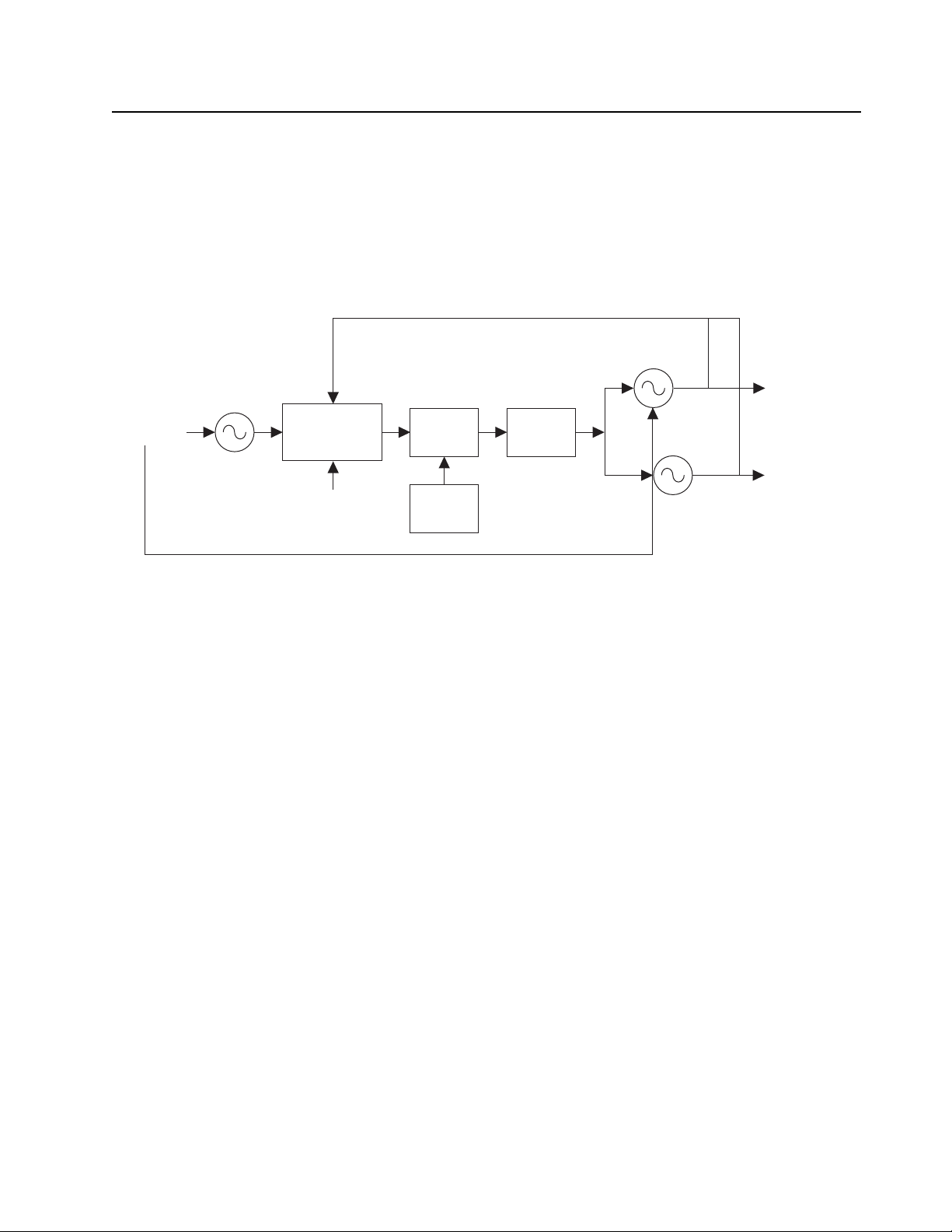
2.2.4 RX Audio Circuit
The RX audio circuit consists of Audio Processor IC, Audio amp, speakers & Sub-tone system.
The RX Audio from U201 is channeled to Audio processor IC. VR3 controls the received
demodulated signal level from -4.0 dB to +3.5 dB in 0.5 dB steps. RX LPF eliminates high-frequency
audio components > 3 kHz. TX/RX HPF eliminates low-frequency audio components lower < 250Hz.
Descrambler (if ON) inverts the spectrum distribution of audio signals with respect to scrambling
frequency. De-emphasis (if ON) restores high-frequency component of audio signal which has been
emphasized by the pre-emphasis circuit in transmitting radio. Expander (if ON) expands audio signal
by 0.5 dB to restore the original signal compressed by transmitting radio. VR4 amplifies RX audio
level by -18.0 dB, with -4.5 dB to +4.5 dB in 0.25 dB steps adjustment range. Smoothing filter (SMF)
eliminates high-frequency and clock components, generated by ASIC.
Sub-audio Programmable LPF totally eliminates voice audio from Audio signal to extract sub-audio
tone. VR5 regulates the output level of extracted sub-audio tone and sends it to a high pass filter
(U105-A,B) with 4 selectable cut-off frequencies and finally passes through a comparator (U105-C),
to square the signal and sends it to the MCU.
The output audio signal of Audio Processor IC is directed to volume control switch (SW/VOL1) which
is controlled by user and is finally amplified by U601BTL Audio Amplifier to a sufficient level to drive
either the external or internal speaker.
Figure 2-4. RX Audio Block Diagram
VR3
Scrambler /
Descrambler
De-
emphasis
Expander VR4 SMF
SVR
IN-
IN+
OUT-
OUT+
Audio Mute
control
RX LPF TX/RX HPF
RXA1
-4 to +3.5dB /
0.5dB
-18, -4.5 to + 4.5dB /
0.25dB
Audio Processor IC (AK2347)
Audio IN
(from IF IC)
VR5
Sub audio
Programmable
LPF
To CPU
(tone detect)
pin 24
pin 18
pin 21
Audio Amp.
U102
U601
Vol1
-6 to +6dB /
0.5dB
INT SPK.
EXT SPK.
J601
Sub audio
HPF
U105-A,B
Compar
ator
U105-C
 Loading...