


Motorola DSP56001RC33, DSP56001RC20, DSP56001FE33, DSP56001FE27, DSP56001FE20 Datasheet
...MOTOROLA
Order this document by DSP56001/D
|
|
SEMICONDUCTOR |
|
|
|
|
|
|
|
|
|
|
|
|
|
|
|
|
|
|
|
|
|
|
|
|
|
|
|
|
|
|
|
|
|
|
|
|
|
|
|
|
|
|
|
|
|
|
|
|
|
|
|
|
|
|
|
|
|
|
|
|
|
|
|
|
|
|
|
|
|
|
|
|
|
|
|
|
|
|
|
|
DSP56001 |
|
||||||||||||||||||||
|
|
TECHNICAL DATA |
|
|
|
|
|
|
|
|
|
|
|
|||||||||||||||||||||
|
24-Bit General Purpose |
Pin Grid Array (PGA) |
|
|
|
|
|
|
|
|
|
|
|
|
|
|||||||||||||||||||
|
Available in an 88 pin ceramic |
|
|
|
|
|
|
|
|
|
|
|
|
|
|
|
|
|
|
|
|
|
||||||||||||
|
Digital Signal Processor |
through-hole package. |
|
|
|
|
|
|
|
|
|
|
|
|
|
|
|
|
|
|
|
|
|
|
|
|
|
|
|
|
|
|
||
|
|
|
|
|
|
|
|
|
|
|
|
|
|
|
|
|
|
|
|
|
|
|
|
|
|
|
|
|
|
|
||||
The DSP56001 is a member of Motorola’s family of
HCMOS, low-power, general purpose Digital Signal Processors. The DSP56001 features 512 words of full speed, on-chip program RAM (PRAM) memory, two
256 word data RAMs, two preprogrammed data
ROMs, and special on-chip bootstrap hardware to permit convenient loading of user programs into the program RAM. It is an off-the-shelf part since the program
memory is user programmable. The core of the processor consists of three execution units operating in parallel — the data ALU, the address generation unit, and the program controller. The DSP56001 has MCU-style on-chip peripherals, program and data memory, as well as a memory expansion port. The MPU-style programming model and instruction set make writing efficient, compact code, straightforward.
The high throughput of the DSP56001 makes it well-suited for communication, high-speed control, numeric processing, computer and audio applications. The key features which facilitate this throughput are:
• |
Speed |
At 16.5 million instructions per second (MIPS) with a 33 MHz clock, the DSP56001 can execute |
|
|
a 1024 point complex Fast Fourier Transform in1.98 milliseconds (66,240 clock cycles). |
• |
Precision |
The data paths are 24 bits wide thereby providing 144 dB of dynamic range; intermediate results |
|
|
held in the 56-bit accumulators can range over 336 dB. |
• |
Parallelism |
The data ALU, address arithmetic units, and program controller operate in parallel so that an in- |
|
|
struction prefetch, a 24x24-bit multiplication, a 56-bit addition, two data moves, and two address |
|
|
pointer updates using one of three types of arithmetic (linear, modulo, or reverse carry) can be |
|
|
executed in a single instruction cycle. This parallelism allows a four coefficient Infinite Impulse Re- |
|
|
sponse (IIR) filter section to be executed in only four cycles, the theoretical minimum for a single |
|
|
multiplier architecture. |
• |
Integration |
In addition to the three independent execution units, the DSP56001 has six on-chip memories, |
|
|
three on-chip MCU style peripherals (Serial Communication Interface, Synchronous Serial Inter- |
|
|
face, and Host Interface), a clock generator and seven buses (three address and four data), mak- |
|
|
ing the overall system functionally complete and powerful, but also very low cost, low power, and |
|
|
compact. |
• |
Invisible Pipeline |
The three-stage instruction pipeline is essentially invisible to the programmer thus allowing |
|
|
straightforward program development in either assembly language or a high-level language such |
|
|
as ANSI C. |
• |
Instruction Set |
The 62 instruction mnemonics are MCU-like making the transition from programming micropro- |
|
|
cessors to programming the DSP56001 digital signal processor as easy as possible. The orthog- |
|
|
onal syntax supports control of the parallel execution units. This syntax provides 12,808,830 dif- |
|
|
ferent instruction variations using the 62 instruction mnemonics. The no-overhead DO instruction |
|
|
and the REPEAT (REP) instruction make writing straight-line code obsolete. |
•DSP56000/DSP56001 Compatibility
The DSP56001 is identical to the DSP56000 except that it has 512x24-bits of on-chip program RAM instead of 3.75K of program ROM; a 32x24-bit bootstrap ROM for loading the program RAM from either a byte-wide memory mapped ROM or via the Host Interface; and the on-chip X and Y Data ROMs have been preprogrammed as positive Muand A-Law to linear expansion tables and a full, four quadrant sine wave table, respectively.
• Low Power |
As a CMOS part, the DSP56001 is inherently very low power; however, three other features can |
|
reduce power consumption to an exceptionally low level. |
|
— The WAIT instruction shuts off the clock in the central processor portion of the DSP56001. |
|
— The STOP instruction halts the internal oscillator. |
|
— Power increases linearly (approximately) with frequency; thus, reducing the clock frequency |
|
reduces power consumption. |
This document contains information on a new product. Specifications and information herein are subject to change without notice.
|
|
|
|
|
|
|
|
|
|
|
|
|
|
|
|
|
|
|
|
|
ã MOTOROLA INC., 1992 |
Rev. 3 |
|
|
|||||
|
|
|
|
|
|
|
|||
May 4, 1998 |
|
||||||||
|
|
|
|
|
|||||

|
|
|
|
YAB |
EXTERNAL ADDRESS |
|
|
|
|
|
|
XAB |
|
||
|
ADDRESS |
|
|
ADDRESS |
|
|
|
|
|
|
PAB |
|
|
||
|
GENERATION |
|
|
|
BUS |
|
|
|
UNIT |
|
|
|
SWITCH |
|
|
|
|
|
|
X MEMORY |
Y MEMORY |
|
|
PORT B |
|
BOOTSTRAP |
PROGRAM |
RAM |
RAM |
|
|
OR HOST |
|
ROM |
RAM |
256X24 |
256X24 |
|
|
15 |
|
32X24 |
512X24 |
μ |
SINE ROM |
|
A |
|
ON-CHIP |
/A ROM |
|
||||
|
|
|
256X24 |
256X24 |
|
PORT |
|
|
PERIPHERALS: |
|
|
|
|||
|
|
|
|
BUS |
7 |
||
9 |
HOST, SSI, |
|
|
|
CONTROL |
||
|
|
|
|
||||
SCI, PI/O |
|
|
|
|
|
||
|
|
|
|
|
|
|
|
PORT C |
|
|
|
|
|
|
|
AND/OR |
|
|
|
|
|
|
|
SSI, SCI |
INTERNAL DATA |
|
|
YDB |
|
|
|
|
|
|
|
|
|
||
|
|
|
|
EXTERNAL |
|
|
|
|
BUS SWITCH |
|
|
XDB |
DATA |
|
|
|
AND BIT |
|
|
PDB |
DATA BUS |
|
|
|
MANIPULATION |
|
|
SWITCH |
|
|
|
|
|
|
|
|
|
||
|
UNIT |
|
|
GDB |
|
|
|
|
|
|
|
|
|
|
|
|
|
|
|
|
|
|
|
|
|
|
|
|
|
|
|
|
|
|
|
|
|
|
|
|
|
|
|
|
|
|
|
|
|
|
|
|
|
|
|
|
|
|
|
|
|
|
|
|
|
|
|
|
|
|
|
|
|
|
|
|
|
|
|
|
|
|
|
|
|
|
|
|
|
|
|
|
|
|
|
|
|
|
|
|
|
|
|
|
|
|
|
|
|
|
|
|
|
|
|
|
|
|
|
|
|
|
|
|
|
|
|
|
|
|
|
|
|
|
|
|
|
|
|
|
PROGRAM |
|
PROGRAM |
|
|
|
|
|
|
|
|
|
|
|
DATA ALU |
|
|||||||||||
|
|
|
|
|
|
|
PROGRAM |
|
|
|
|
|
24X24+56→56-BIT MAC |
|
|||||||||||||||||
|
|
|
|
|
ADDRESS |
|
DECODE |
INTERRUPT |
|
|
|
|
|
|
|||||||||||||||||
|
CLOCK |
|
|
GENERATOR |
|
CONTROLLER |
CONTROLLER |
|
|
|
|
TWO 56-BIT ACCUMULATORS |
|
||||||||||||||||||
GENERATOR |
|
|
|
|
|
|
|
|
|||||||||||||||||||||||
|
|
|
|
|
|
|
|
|
|
|
|
|
|
|
|
|
|
|
|
|
|
|
|
|
|
|
|
|
|||
|
|
|
|
|
|
|
|
|
|
|
|
|
|
|
|
|
|
|
|
|
|
|
|
|
|
|
|
|
|||
|
|
|
|
|
|
|
|
|
|
|
|
|
|
|
|
|
|
|
|
|
|
|
|
|
|
|
|
|
|
|
|
|
|
|
|
|
|
|
|
|
|
|
|
|
|
|
|
|
MODB/IRQB |
|
|
|
|
|
|
|
|
|
16 BITS |
||||
|
|
|
|
|
|
|
|
|
|
|
|
|
|
|
|
|
|
|
|
|
|
|
|
|
|
|
|
|
|
||
EXTAL XTAL |
|
|
|
|
|
|
|
|
|
|
|
|
MODA/IRQA |
|
|
|
|
|
|
|
|
|
24 BITS |
||||||||
|
|
|
|
|
|
|
|
|
|
|
|
|
|
|
|
|
|
|
|
|
|
|
|
|
|
||||||
|
|
|
|
|
|
|
|
|
|
|
|
|
|
|
|
|
|
|
|
|
|
|
|
|
|
|
|
|
|
|
|
|
|
|
|
|
|
|
|
|
|
|
|
|
|
|
|
|
|
RESET |
|
|
|
|
|
|
|
|
|
|
|
||
|
|
|
|
|
|
|
|
|
|
|
|
|
|
|
|
|
|
|
|
|
|
|
|
|
|
|
|
||||
Figure 1. DSP56001 Block Diagram
In the USA:
For technical assistance call:
DSP Applications Helpline (512) 891-3230
For availability and literature call your local Motorola Sales Office or Authorized Motorola Distributor.
For free application software and information call the Dr. BuB electronic bulletin board: 9600/4800/2400/1200/300 baud
(512) 891-3771
(8 data bits, no parity, 1 stop)
In Europe, Japan and Asia Pacific
Contact your regional sales office or Motorola distributor.
MOTOROLA |
DSP56001 |
2 |
|

SIGNAL DESCRIPTION
The DSP56001 is available in 132 pin surface mount (CQFP and PQFP) or an 88-pin pin-grid array packaging. Its input and output signals are organized into seven functional groups which are listed below and shown in Figure 1.
Port A Address and Data Buses
Port A Bus Control
Interrupt and Mode Control
Power and Clock
Host Interface or Port B I/O
Serial Communications Interface or Port C I/O
Synchronous Serial Interface or Port C I/O
PORT A ADDRESS AND DATA BUS
Address Bus (A0-A15)
These three-state output pins specify the address for external program and data memory accesses. To minimize power dissipation, A0-A15 do not change state when external memory spaces are not being accessed.
Data Bus (D0-D23)
These pins provide the bidirectional data bus for external program and data memory accesses. D0-D23 are in the high-impedance state when the bus grant signal is asserted.
Read Enable (RD)
This three-state output is asserted to read external memory on the data bus D0-D23. This pin is three-stated during RESET.
Write Enable (WR)
This three-state output is asserted to write external memory on the data bus D0-D23. This pin is three-stated during RESET.
Bus Request (BR/WT)
The bus request input BR allows another device such as a processor or DMA controller to become the master of external data bus D0-D23 and external address bus A0-A15. When operating mode register (OMR) bit 7 is clear and BR is asserted, the DSP56001 will always release the external data bus D0-D23, address bus A0-A15, and bus control pins PS, DS, X/Y, RD, and WR (i. e., Port A), by placing these pins in the high-impedance state after execution of the current instruc-
tion has been completed. The BR pin should be pulled up when not in use.
If OMR bit 7 is set, this pin is an input that allows an external device to force wait states during an external Port A operation for as long as WT is asserted.
Bus Grant (BG/BS)
If OMR bit 7 is clear, this output is asserted to acknowledge an external bus request after Port A has been released. If OMR bit 7 is set, this pin is bus strobe and is asserted when the DSP accesses Port A. This pin is three-stated during RESET.
PORT A BUS CONTROL
Program Memory Select (PS)
This three-state output is asserted only when external program memory is referenced. This pin is three-stated during RESET.
Data Memory Select (DS)
This three-state output is asserted only when external data memory is referenced. This pin is three-stated during RESET.
X/Y Select (X/Y)
This three-state output selects which external data memory space (X or Y) is referenced by data memory select (DS). This pin is three-stat- ed during RESET.
|
|
|
|
|
|
|
|
|
|
|
|
|
|
|
|
|
|
|
|
|
|
HOST CONTROL |
|
|
|
|
|
|
|
|
|
||||||||||||||||
|
|
|
|
|
|
HOST DATA |
H0-H7 |
HA0 |
|
HA1 |
|
HA2 |
|
|
HR/W |
|
|
HEN |
|
|
|
HREQ |
|
HACK |
|
||||||||||||||||||||||
|
|
|
|
|
|
|
|
|
|
|
|
|
|
|
|
|
|||||||||||||||||||||||||||||||
|
|
|
|
|
|
|
|
|
|
|
|
|
|||||||||||||||||||||||||||||||||||
|
|
|
|
|
|
|
|
|
|
|
|
|
|||||||||||||||||||||||||||||||||||
|
|
|
|
|
|
|
|
BUS |
|
|
|
|
|
|
|
|
|
|
|
|
|
|
|
|
|
|
|
|
|
|
|
|
|
|
|
|
|
|
|
RXD |
|
||||||
|
|
|
|
|
|
|
|
|
|
|
|
|
|
|
|
|
|
|
|
|
|
|
|
|
|
|
|
|
|
|
|
|
|
|
|
|
|
|
|
||||||||
ADDRESS A0-A15 |
|
|
|
|
|
|
|
|
|
|
|
|
|
|
|
|
|
|
|
|
|
|
|
|
|
|
|
|
|
|
|
|
|
|
|
|
|
||||||||||
|
|
|
|
|
|
|
|
|
|
|
|
|
|
|
|
|
|
|
|
|
|
|
|
|
|
|
|
|
|
|
|
|
|
|
|
|
|||||||||||
|
|
|
|
|
|
|
|
|
|
|
|
|
|
|
|
|
|
|
|
|
|
|
|
|
|
|
|
|
|
|
|
|
|
|
|
|
|||||||||||
DATA |
D0-D23 |
|
|
|
|
|
|
|
|
|
|
|
|
|
PORT B |
|
|
|
|
|
|
|
|
|
|
|
|
|
|
|
|
TXD |
SCI |
||||||||||||||
|
|
|
|
|
|
|
|
|
|
|
|
|
|
|
|
|
|
|
|
|
|
|
|
|
|
|
|
|
|
|
|
|
|
|
|
|
|
|
|
|
|
|
|
|
|
|
|
|
|
|
|
|
PS |
|
|
|
|
|
|
|
|
|
|
|
|
|
|
|
|
|
|
|
|
|
|
|
|
|
|
|
|
|
|
|
|
SCLK |
|
||||||||
|
|
|
|
|
|
|
|
|
|
|
|
|
|
|
|
|
|
|
|
|
|
|
|
|
|
|
|
|
|
|
|
|
|
|
|
|
|
|
|
|
|||||||
|
|
|
|
|
|
|
|
|
|
|
|
|
|
|
|
|
|
|
|
|
|
|
|
|
|
|
|
|
|
|
|
|
|
|
|
|
|
|
|
|
|
|
|
|
|||
|
|
|
|
|
|
|
|
|
|
|
|
|
|
|
|
|
|
|
|
|
|
|
|
|
|
|
|
|
|
|
|
|
|
|
|
|
|
|
|
|
|
|
|
|
|
|
|
|
|
|
|
|
DS |
|
|
PORT A |
|
|
|
|
|
|
|
|
|
PORT C |
|
|
|
|
SC0 |
|
|||||||||||||||||||||||
|
|
|
|
|
|
|
|
|
|
|
|
|
|
|
|
|
|
|
|
|
|
|
|
|
|
|
|
||||||||||||||||||||
|
|
|
|
|
|
|
|
|
|
|
|
|
|
|
|
|
|
|
|
|
|
|
|
|
|
|
|
|
|
||||||||||||||||||
|
|
|
|
|
|
|
|
|
|
|
|
|
|
|
|
|
|
|
|
|
|
|
|
|
|
|
|
|
|
|
|||||||||||||||||
BUS |
|
|
|
|
RD |
|
|
|
|
|
|
|
|
|
|
|
|
|
|
SC1 |
|
||||||||||||||||||||||||||
|
|
|
|
|
|
|
|
|
|
|
|
|
|
|
|
|
|
|
|
|
|
|
|
|
|
||||||||||||||||||||||
|
|
|
|
|
|
|
|
|
|
|
|
|
|
|
|
|
|
|
|
|
|
|
|
|
|
|
|
|
|
|
|
|
|
|
|
|
|
|
|
|
|
|
|
|
|
||
|
|
|
|
|
|
|
|
|
|
|
|
|
|
|
|
|
|
|
|
|
|
|
|
|
|
|
|
|
|
|
|
|
|
|
|
|
|
|
|
|
|
|
|
|
|
|
|
CONTROL |
|
|
|
WR |
|
|
|
|
|
|
|
|
|
|
|
|
|
|
DSP56001 |
|
|
|
|
|
|
|
|
|
|
|
|
SCK |
SSI |
||||||||||||||
|
|
|
|
|
|
|
|
|
|
|
|
|
|
|
|
|
|
|
|
|
|
|
|
|
|
|
|
|
|||||||||||||||||||
|
|
|
|
|
|
|
|
|
|
|
|
|
|
|
|
|
|
|
|
|
|
|
|
|
|
|
|
|
|
|
|
||||||||||||||||
|
|
|
|
|
|
|
|
|
|
|
|
|
|
|
|
|
|
|
|
|
|
|
|
|
|
|
|
|
|
|
|
|
|
||||||||||||||
|
|
|
|
|
X/Y |
|
|
|
|
|
|
|
|
|
|
|
|
|
|
|
|
|
|
|
|
|
|
|
|
|
|
|
|
|
|
|
|
|
|
|
|
|
|
|
SRD |
|
|
|
|
|
|
|
|
|
|
|
|
|
|
|
|
|
|
|
|
|
|
|
|
|
|
|
|
|
|
|
|
|
|
|
|
|
|
|
|
|
|
|
|
|
|
|
|||
|
|
|
|
|
|
|
|
|
|
|
|
|
|
|
|
|
|
|
|
|
|
|
|
|
|
|
|
|
|
|
|
|
|
|
|
|
|
|
|
|
|
|
|
|
|
|
|
|
|
|
|
|
|
|
|
|
|
|
|
|
|
|
|
|
|
|
|
|
|
|
|
|
|
|
|
|
|
|
|
|
|
|
|
|
|
|
|
|
|
|
|
|
|
|
|
|
|
BR/WT |
|
|
|
|
|
|
|
|
|
|
|
|
|
|
|
|
|
|
|
|
|
|
|
|
|
|
|
|
|
|
|
|
|
|
STD |
|
|||||||||
|
|
|
|
|
|
|
|
|
|
|
|
|
|
|
|
|
|
|
|
|
|
|
|
|
|
|
|
|
|
|
|
|
|
|
|
||||||||||||
|
|
|
|
|
|
|
|
|
|
|
|
|
|
|
|
|
|
|
|
|
|
|
|
|
|
|
|
|
|
|
|
|
|
|
|
|
|
|
|
|
|
|
|
|
|
|
|
|
|
|
|
|
|
|
|
|
|
|
|
|
|
|
|
|
|
|
|
|
|
|
|
|
|
|
|
|
|
|
|
|
|
|
|
|
|
|
|
|
|
|
|
|
|
|
|
|
|
BG/BS |
|
|
|
|
|
|
|
|
|
|
|
|
|
|
|
|
|
|
|
|
|
|
|
|
|
|
|
|
|
|
|
|
|
|
|
||||||||||
|
|
|
|
|
|
|
|
|
|
|
|
|
|
|
|
|
|
|
|
|
|
|
|
|
|
|
|
|
|
|
|
|
|
|
|
|
|||||||||||
|
|
|
|
|
|
|
|
|
|
|
|
|
|
|
|
|
|
|
|
|
|
|
|
|
|
|
|
|
|
|
|
|
|
|
|
|
|
|
|
|
|
|
|
|
|
|
|
|
|
|
|
|
|
|
|
|
|
|
|
|
|
|
|
|
|
|
|
|
|
|
|
|
|
|
|
|
|
|
|
|
|
|
|
|
|||||||||||
|
|
|
|
|
|
|
|
|
|
|
|
|
|
|
|
|
|
|
|
|
|
|
|
|
|
|
|
|
|
|
|
|
|
|
|
|
|
|
|
|
|
|
|
|
|
|
|
|
|
|
|
|
|
|
|
|
|
|
|
|
|
|
|
|
|
|
|
|
|
|
|
|
|
|
|
|
|
|
|
|
|
|
|
|
|
|
|
|
|
|
|
|
|
|
|
|
|
|
|
|
|
|
|
|
|
|
|
|
|
|
|
VSS |
|
|
VDD |
XTAL |
EXTAL |
|
RESET |
|
|
MODB/ |
|
IRQB |
MODA/ |
|
IRQA |
|
|||||||||||||||
|
|
|
|
|
|
|
|
|
|
|
|
|
|
|
|
|
|
|
|
|
|
|
|
||||||||||||||||||||||||
|
|
|
|
|
|
|
|
|
|
|
|
|
|
|
|
|
|
|
|
|
|
|
|
|
|
|
|
|
|
|
|
||||||||||||||||
INTERRUPT AND MODE CONTROL
Mode Select A/External Interrupt Request A (MODA/IRQA),
Mode Select B/External Interrupt Request B (MODB/IRQB)
These two inputs have dual functions: 1) to select the initial chip operating mode and 2) to receive an interrupt request from an external source. MODA and MODB are read and internally latched in the DSP when the processor exits the RESET state. Therefore these two pins should be forced into the proper state during reset. After leaving the RESET state, the MODA and MODB pins automatically change to external interrupt requests IRQA and IRQB. After leaving the reset state the chip operating mode can be changed by software. IRQA and IRQB may be programmed to be level sensitive or negative edge triggered. When edge triggered, triggering occurs at a voltage level and is not directly related to the fall time of the interrupt signal, however, the probability of noise on IRQA or IRQB generating multiple interrupts increases with increasing fall time of the interrupt signal. These pins are inputs during RESET.
Reset (RESET)
This Schmitt trigger input pin is used to reset the DSP56001. When RESET is asserted, the DSP56001 is initialized and placed in the reset
state. When the RESET signal is deasserted, the initial chip operating mode is latched from the MODA and MODB pins. When coming out of reset, deassertion occurs at a voltage level and is not directly related to the rise time of the reset signal; however, the probability of noise on
RESET generating multiple resets increases with increasing rise time of the reset signal.
POWER AND CLOCK
Power (Vcc), Ground (GND)
There are five sets of power and ground pins used for the four groups of logic on the chip, two pairs for internal logic, one power and two ground for Port A address and control pins, one power and two ground for Port A data pins, and one pair for peripherals. Refer to the pin assignments in the LAYOUT PRACTICES section.
Figure 2. Functional Signal Groups |
|
DSP56001 |
MOTOROLA |
|
3 |

External Clock/Crystal Input (EXTAL)
EXTAL may be used to interface the crystal oscillator input to an external crystal or an external clock.
Crystal Output (XTAL)
This output connects the internal crystal oscillator output to an external crystal. If an external clock is used, XTAL should not be connected.
HOST INTERFACE
Host Data Bus (H0-H7)
This bidirectional data bus is used to transfer data between the host processor and the DSP56001. This bus is an input unless enabled by a host processor read. H0-H7 may be programmed as general purpose parallel I/O pins called PB0-PB7 when the Host Interface is not being used. These pins are configured as a GPIO input pins during hardware reset.
Host Address (HA0-HA2)
These inputs provide the address selection for each Host Interface register. HA0-HA2 may be programmed as general purpose parallel I/O pins called PB8-PB10 when the Host Interface is not being used. These pins are configured as a GPIO input pins during hardware reset.
Host Read/Write (HR/W)
This input selects the direction of data transfer for each host processor access. HR/W may be programmed as a general purpose I/O pin called PB11 when the Host Interface is not being used. This pin is configured as a GPIO input pins during hardware reset.
Host Enable (HEN)
This input enables a data transfer on the host data bus. When HEN is asserted and HR/W is high, H0-H7 become outputs, and DSP56001 data may be read by the host processor, When HEN is asserted and HR/W is low, H0-H7 become inputs and host data is latched inside the DSP when HEN is deasserted. Normally a chip select signal, derived from host address decoding and an enable clock, is used to generate HEN. HEN may be programmed as a general purpose I/O pin called PB12 when the Host Interface is not being used. This pin is configured as a GPIO input pins during hardware reset.
Host Request (HREQ)
This open-drain output signal is used by the DSP56001 Host Interface to request service from the host processor, DMA controller, or simple external controller. HREQ may be programmed as a general purpose I/O pin (not open-drain) called PB13 when the Host interface is not being used. HREQ should be pulled high when not in use. This pin is configured as a GPIO input pins during hardware reset.
Host Acknowledge (HACK)
This input has two functions: 1) to receive a Host Acknowledge handshake signal for DMA transfers and, 2) to receive a Host Interrupt Acknowledge compatible with MC68000 Family processors. HACK may be programmed as a general purpose I/O pin called PB14 when the Host Interface is not being used. This pin is configured as a GPIO input pins during hardware reset. HACK should be pulled high when not in use.
SERIAL COMMUNICATIONS INTERFACE (SCI)
Receive Data (RXD)
This input receives byte-oriented data into the SCI Receive Shift Register. Input data is sampled on the positive edge of the Receive Clock. RXD may be programmed as a general purpose I/O pin called PC0 when the SCI is not being used. This pin is configured as a GPIO input pins during hardware reset.
Transmit Data (TXD)
This output transmits serial data from the SCI Transmit Shift Register. Data changes on the negative edge of the transmit clock. This output is stable on the positive edge of the transmit clock. TXD may be programmed as a general purpose I/O pin called PC1 when the SCI is not being used. This pin is configured as a GPIO input pins during hardware reset.
SCI Serial Clock (SCLK)
This bidirectional pin provides an input or output clock from which the transmit and/or receive baud rate is derived in the asynchronous mode and from which data is transferred in the synchronous mode. SCLK may be programmed as a general purpose I/O pin called PC2 when the SCI is not being used. This pin is configured as a GPIO input pins during hardware reset.
SYNCHRONOUS SERIAL INTERFACE (SSI)
Serial Control Zero (SC0)
This bidirectional pin is used for control by the SSI. SC0 may be programmed as a general purpose I/O pin called PC3 when the SSI is not being used. This pin is configured as a GPIO input pins during hardware reset.
Serial Control One (SC1)
This bidirectional pin is used for control by the SSI. SC1 may be programmed as a general purpose I/O pin called PC4 when the SSI is not being used. This pin is configured as a GPIO input pins during hardware reset.
Serial Control Two (SC2)
This bidirectional pin is used for control by the SSI. SC2 may be programmed as a general purpose I/O pin called PC5 when the SSI is not being used. This pin is configured as a GPIO input pins during hardware reset.
SSI Serial Clock (SCK)
This bidirectional pin provides the serial bit rate clock for the SSI when only one clock is used. SCK may be programmed as a general purpose I/O pin called PC6 when the SSI is not being used. This pin is configured as a GPIO input pins during hardware reset.
SSI Receive Data (SRD)
This input pin receives serial data into the SSI Receive Shift Register. SRD may be programmed as a general purpose I/O pin called PC7 when the SSI is not being used. This pin is configured as a GPIO input pins during hardware reset.
SSI Transmit Data (STD)
This output pin transmits serial data from the SSI Transmit Shift Register. STD may be programmed as a general purpose I/O pin called PC8 when the SSI is not being used. This pin is configured as a GPIO input pins during hardware reset.
MOTOROLA |
DSP56001 |
4 |
|
DSP56001 Electrical Characteristics
Electrical Specifications
The DSP is fabricated in high density CMOS with TTL compatible inputs and outputs.
Maximum Ratings (VSS = 0 Vdc)
Rating |
Symbol |
Value |
Unit |
|
|
|
|
Supply Voltage |
Vcc |
-0.3 to +7.0 |
V |
|
|
|
|
All Input Voltages |
Vin |
VSS- 0.5 to Vcc + 0.5 |
V |
|
|
|
|
Current Drain per Pin |
I |
10 |
mA |
excluding Vcc and VSS |
|
|
|
Operating Temperature Range |
TJ |
-40 to +105 |
°C |
|
|
|
|
Storage Temperature |
Tstg |
-55 to +150 |
°C |
|
|
|
|
Maximum Electrical Ratings
Thermal Characteristics - PGA Package
|
Characteristics |
Symbol |
Value |
Rating |
|
Thermal Resistance - Ceramic |
|
|
|
|
|
|
|
|
|
Junction to Ambient |
ΘJA |
27 |
°C/W |
|
Junction to Case (estimated) |
ΘJC |
6.5 |
°C/W |
Thermal Characteristics - CQFP Package |
|
|
|
|
|
Characteristics |
Symbol |
Value |
Rating |
|
Thermal Resistance - Ceramic |
|
|
|
|
|
|
|
|
|
Junction to Ambient |
ΘJA |
40 |
°C/W |
|
Junction to Case (estimated) |
ΘJC |
7.0 |
°C/W |
|
|
|
|
|
Thermal Characteristics - PQFP Package |
|
|
|
|
|
Characteristics |
Symbol |
Value |
Rating |
|
Thermal Resistance - Plastic |
|
|
|
|
|
|
|
|
|
Junction to Ambient |
ΘJA |
38 |
°C/W |
|
Junction to Case (estimated) |
ΘJC |
13.0 |
°C/W |
|
|
|
|
|
This device contains circuitry protecting against damage due to high static voltage or electrical fields; however, it is advised that normal precautions be taken to avoid application of any voltages higher than maximum-rated voltages to this high-impedance circuit. Reliability of operation is enhanced if unused inputs are tied to an appropriate logic voltage level (e.g., either Gnd or Vcc).
DSP56001 |
MOTOROLA |
|
5 |
DSP56001 Electrical Characteristics |
|
Power Considerations |
|
The average chip-junction temperature, TJ, in °C can be obtained from: |
|
TJ = TA + (PD × ΘJA) |
(1) |
Where:
TA = Ambient Temperature, °C
ΘJA = Package Thermal Resistance, Junction-to-Ambient, °C/W
PD = PINT + PI/O
PINT = ICC × Vcc, Watts - Chip Internal Power
PI/O = Power Dissipation on Input and Output Pins - User Determined
For most applications PI/O << PINT and can be neglected; however, PI/O + PINT must not exceed Pd. An appropriate relationship
between PD and TJ (if PI/O is neglected) is: |
|
|||||
PD = K/(TJ + 273° C) |
|
|
|
(2) |
||
Solving equations (1) and (2) for K gives: |
|
|||||
K = P × (T |
A |
+ 273° C) + Θ |
JA |
× P |
2 |
(3) |
D |
|
|
D |
|
||
Where K is a constant pertaining to the particular part. K can be determined from equation (2) by measuring PD (at equilibrium) for a known TA. Using this value of K, the values of PD and TJ can be obtained by solving equations (1) and (2) iteratively for any value of TA. The total thermal resistance of a package (ΘJA) can be separated into two components, ΘJC and CA, representing the barrier to heat flow from the semiconductor junction to the package (case) surface (ΘJC) and from the case to the outside ambient (CA). These terms are related by the equation:
ΘJA = ΘJC + CA |
(4) |
ΘJC is device related and cannot be influenced by the user. However, CA is user dependent and can be minimized by such thermal management techniques as heat sinks, ambient air cooling, and thermal convection. Thus, good thermal management on the part of the user can significantly reduce CA so that ΘJA approximately equals ΘJC. Substitution of ΘJC for ΘJA in equation (1) will result in a lower semiconductor junction temperature. Values for thermal resistance presented in this document, unless estimated, were derived using the procedure described in Motorola Reliability Report 7843, “Thermal Resistance Measurement Method for MC68XX Microcomponent Devices”, and are provided for design purposes only. Thermal measurements are complex and dependent on procedure and setup. User-derived values for thermal resistance may differ.
Layout Practices
Each Vcc pin on the DSP56001 should be provided with a low-impedance path to + 5 volts. Each GND pin should likewise be provided with a low-impedance path to ground. The power supply pins drive four distinct groups of logic on chip. They are:
Vcc |
GND |
Function |
|
|
|
G12,C6 |
G11,B7 |
Internal Logic supply pins |
L8 |
L6,L9 |
Address bus output buffer supply pins |
G3 |
D3,J3 |
Data bus output buffer supply pins |
C9 |
E11 |
Port B and C output buffer supply pins |
|
|
|
|
Power and Ground Connections for PGA |
|
|
|
|
Vcc |
GND |
Function |
|
|
|
35, 36, 128, 129 |
33, 34, 130, 131 |
Internal Logic supply pins |
63, 64 |
55, 56, 73, 74 |
Address bus output buffer supply pins |
100, 101 |
90, 91, 111, 112 |
Data bus output buffer supply pins |
12, 13 |
23, 24 |
Port B and C output buffer supply pins |
|
|
|
|
Power and Ground Connections for CQFP and PQFP |
MOTOROLA |
DSP56001 |
6 |
|

DSP56001 Electrical Characteristics
Power and Ground Connections
The Vcc power supply should be bypassed to ground using at least four 0.1 uF bypass capacitors located either underneath the chip or as close as possible to the four sides of the package. The capacitor leads and associated printed circuit traces connecting to chip Vcc and Gnd should be kept to less than 1/2" per capacitor lead. A four-layer board is recommended, employing two inner layers as Vcc and Gnd planes. All output pins on the DSP56001 have fast rise and fall times — typically less than 3 ns. with a 10 pf. loa d. Printed circuit (PC) trace interconnection length should be minimized in order to minimize undershoot and reflections caused by these fast output switching times. This recommendation particularly applies to the address and data buses as well as the RD, WR, IRQA, IRQB, and HEN pins. Maximum PC trace lengths on the order of 6" are recommended. Capacitance calculations should consider all device loads as well as parasitic capacitances due to the PC traces. Attention to proper PCB layout and bypassing becomes especially critical in systems with higher capacitive loads because these loads create higher transient currents in the Vcc and GND circuits. Pull up/down all unused inputs or signals that will be inputs during reset.
Signal Stability
When designing hardware to interface with the Host Interface, it is important to ensure that all signals be clean and free from noise. Particular attention should be given to the quality of the Host Enable (HEN). All inputs to the port should be stable when HEN is asserted and should remain stable until HEN has fully returned to the deasserted state. It is important to note that such phenomena as ground-bounce and cross-talk can inadvertently cause HEN to temporarily rise above Vil max. Should this occur without completing the full logic transition to Vih min, the DSP56001 Host Port may not correctly update the port status information which can result in storing two or more copies of a single down loaded data word. Of course, if a full logic transition occurs, the part will complete a normal data transfer operation.
DSP56001 |
MOTOROLA |
|
7 |
DSP56001 Electrical Characteristics
DC Electrical Characteristics (Vcc = 5.0 Vdc + 10%; TJ = -40 to +105° C at 20.5 MHz and 27 MHz) (Vcc = 5.0 Vdc + 5%; TJ = -40 to +105° C at 33 MHz)
|
|
|
|
|
|
|
Characteristic |
|
Symbol |
Min |
Typ |
Max |
Unit |
||||||||||||||||||||||
|
|
|
|
|
|
|
|
||||||||||||||||||||||||||||
Supply Voltage |
20, 27 MH z |
|
Vcc |
4.5 |
5.0 |
5.5 |
V |
||||||||||||||||||||||||||||
|
|
|
|
|
|
|
|
|
|
33 MHz |
|
|
4.75 |
|
5.25 |
|
|||||||||||||||||||
|
|
|
|
|
|
|
|
|
|
|
|
|
|
|
|
|
|
|
|
|
|
|
|
|
|
|
|
|
|||||||
Input High Voltage |
|
|
|
|
|
|
|
|
|
|
|
|
|
|
|
|
|
|
|
|
|
|
|
|
VIH |
2.0 |
— |
Vcc |
V |
||||||
Except EXTAL, |
RESET, |
|
MODA/IRQA, |
|
MODB/IRQB |
|
|
|
|
|
|
||||||||||||||||||||||||
|
|
|
|
|
|
|
|
|
|
|
|
|
|
|
|
|
|
|
|
|
|
|
|
|
|
|
|
|
|||||||
Input Low Voltage |
|
|
|
|
|
|
|
|
|
|
|
|
|
|
|
|
|
|
|
|
|
|
|
VIL |
-0.5 |
— |
0.8 |
V |
|||||||
Except EXTAL, MODA/IRQA, |
|
MODB/IRQB |
|
|
|
|
|
|
|||||||||||||||||||||||||||
|
|
|
|
|
|
|
|
|
|
|
|
|
|
|
|
||||||||||||||||||||
Input High Voltage |
|
|
|
|
|
|
|
|
EXTAL |
|
VIHC |
4.0 |
— |
Vcc |
V |
||||||||||||||||||||
Input Low Voltage |
|
|
|
|
|
|
|
|
EXTAL |
|
VILC |
-0.5 |
— |
0.6 |
V |
||||||||||||||||||||
Input High Voltage |
|
|
|
|
|
|
|
|
|
|
|
|
|
|
|
|
|
|
|
|
VIHR |
2.5 |
— |
Vcc |
V |
||||||||||
|
|
|
|
|
|
|
|
RESET |
|||||||||||||||||||||||||||
Input High Voltage |
|
|
|
|
|
|
|
|
|
|
|
|
|
|
|
|
|
|
|
|
|
|
|
VIHM |
3.5 |
— |
Vcc |
V |
|||||||
|
MODA/IRQA |
and MODB/IRQB |
|||||||||||||||||||||||||||||||||
Input Low Voltage |
|
|
|
|
|
|
|
|
|
|
|
|
|
|
|
|
|
|
|
|
|
|
|
VILM |
-0.5 |
— |
2.0 |
V |
|||||||
|
MODA/IRQA |
and MODB/IRQB |
|||||||||||||||||||||||||||||||||
Input Leakage Current |
|
|
|
|
|
|
|
|
|
|
|
|
|
|
|
|
|
|
|
|
|
|
|
Iin |
-1 |
— |
1 |
uA |
|||||||
EXTAL, |
|
|
|
|
|
|
|
|
|
|
|
|
|
|
|||||||||||||||||||||
RESET, |
MODA/IRQA, |
MODB/IRQB, |
BR |
|
|
|
|
|
|
||||||||||||||||||||||||||
|
|
|
|
|
|
|
|||||||||||||||||||||||||||||
Three-State (Off-State) Input Current |
|
ITSI |
-10 |
— |
10 |
uA |
|||||||||||||||||||||||||||||
(@2.4 V/0.4 V) |
|
|
|
|
|
|
|
|
|
|
|
|
|
|
|
|
|
|
|
|
|
|
|
|
|
|
|
|
|||||||
|
|
|
|
|
|
|
|
|
|
||||||||||||||||||||||||||
Output High Voltage |
|
|
(IOH = -0.4 mA) |
|
VOH |
2.4 |
— |
— |
V |
||||||||||||||||||||||||||
Output Low Voltage |
|
|
(IOL = 1.6 mA; |
|
VOL |
— |
— |
0.4 |
V |
||||||||||||||||||||||||||
|
RD, |
|
WR |
IOL = 1.6 mA; Open Drain |
|
|
|
|
|
|
|||||||||||||||||||||||||
|
HREQ |
IOL = 6.7 mA, TXD IOL = 6.7 mA) |
|
|
|
|
|
|
|||||||||||||||||||||||||||
Total Supply Current |
|
|
|
5.25 V, 33 MHz |
|
IDD33 |
— |
160 |
185 |
mA |
|||||||||||||||||||||||||
|
|
|
|
|
|
|
|
|
|
5 . 5 V, 27 MHz |
|
IDD27 |
— |
130 |
155 |
mA |
|||||||||||||||||||
|
|
|
|
|
|
|
|
|
|
5 . 5 V, 20 MHz |
|
IDD20 |
— |
100 |
115 |
mA |
|||||||||||||||||||
|
|
|
|
|
|
|
|
in WAIT Mode (see Note 1) |
|
IDDW |
— |
10 |
25 |
mA |
|||||||||||||||||||||
|
|
|
|
|
|
|
|
in STOP Mode (see Note 1) |
|
IDDS |
— |
100 |
2000 |
μA |
|||||||||||||||||||||
Input Capacitance |
|
|
|
|
(see Note 2) |
|
Cin |
— |
10 |
— |
pf |
||||||||||||||||||||||||
|
|
|
|
|
|
|
|
|
|
|
|
|
|
|
|
|
|
|
|
|
|
|
|
|
|
|
|
|
|
|
|
|
|
|
|
Notes:
1.In order to obtain these results all inputs must be terminated (i.e., not allowed to float).
2.Periodically sampled and not 100% tested.
MOTOROLA |
DSP56001 |
8 |
|

DSP56001 Electrical Characteristics
AC Electrical Characteristics
The timing waveforms in the AC Electrical Characteristics are tested with a VIL maximum of 0.5 V and a VIH minimum of 2.4 V for
all pins, except EXTAL, RESET, MODA, and MODB. These four pins are tested using the input levels set forth in the DC Electrical Characteristics. AC timing specifications which are referenced to a device input signal are measured in production with respect to the 50% point of the respective input signal’s transition. DSP56001 output levels are measured with the production test machine VOL and VOH reference levels set at 0.8 V and 2.0 V respectively.
AC Electrical Characteristics - Clock Operation
The DSP56001 system clock may be derived from the on-chip crystal oscillator as shown in Clock Figure 1, or it may be externally supplied. An externally supplied square wave voltage source should be connected to EXTAL, leaving XTAL physically unconnected (see Clock Figure 2) to the board or socket. The rise and fall time of this external clock should be 5 ns maximum.
Num |
Characteristics |
20.5 MHz |
27 MHz |
33 MHz |
Unit |
|||||||
|
|
|
Min |
|
Max |
Min |
|
Max |
Min |
|
Max |
|
|
|
|
|
|
|
|
||||||
|
|
|
|
|
|
|
|
|
|
|
|
|
|
Frequency of Operation (EXTAL Pin) |
4.0 |
|
20.5 |
4.0 |
|
27.0 |
4.0 |
|
33.0 |
MHz |
|
|
|
|
|
|
|
|
|
|
|
|
||
|
|
|
|
|
|
|
|
|
|
|
|
|
1 |
External Clock Input High (tch) — |
22 |
|
150 |
17 |
|
150 |
13.5 |
|
150 |
ns |
|
|
|
|
|
|
|
|
|
|
|
|
||
|
EXTAL Pin |
(see Note 1 and 2) |
|
|
|
|
|
|
|
|
|
|
|
|
|
|
|
|
|
|
|
|
|
|
|
2 |
External Clock Input Low (tcl) — |
22 |
|
150 |
17 |
|
150 |
13.5 |
|
150 |
ns |
|
|
|
|
|
|
|
|
|
|
|
|
||
|
EXTAL Pin |
(see Note 1 and 2) |
|
|
|
|
|
|
|
|
|
|
|
|
|
|
|
|
|
|
|
|
|
|
|
3 |
Clock Cycle Time = cyc = 2T |
48.75 |
|
250 |
37 |
|
250 |
30.33 |
|
250 |
ns |
|
|
|
|
|
|
|
|
|
|
|
|
||
|
|
|
|
|
|
|
|
|
|
|
|
|
4 |
Instruction Cycle Time = Icyc = 4T |
97.5 |
|
500 |
74 |
|
500 |
60 |
|
500 |
ns |
|
|
|
|
|
|
|
|
|
|
|
|
||
|
|
|
|
|
|
|
|
|
|
|
|
|
Notes:
1.External Clock Input High and External Clock Input Low are measured at 50% of the input transition. tch and tcl are dependent on the duty cycle.
2.T = Icyc / 4 is used in the electrical characteristics. T represents an average which is independent of the duty cycle.
DSP56001 |
MOTOROLA |
|
9 |

DSP56001 Electrical Characteristics
XTAL EXTAL
|
R |
• |
• |
• |
• |
C |
C |
|
XTAL1 |
Fundamental Frequency
Crystal Oscillator
Suggested Component Values
For fosc = 4 MHz:
R = 680 KΩ + 10% C = 20 pf + 20%
For fosc = 30 MHz:
R = 680 KΩ + 10%
C = 20 pf + 20%
Notes:
(1) The suggested crystal source is ICM,
# 433163 - 4.00 (4MHz fundamental, 20 pf load) or # 436163 - 30.00 (30 MHz fundamental, 20 pf load).
|
|
|
|
|
EXTAL |
|
|
|
|
|
|
|
|
|
|
|
|
|
XTAL |
|
||||||||||||
|
|
|
|
|
|
|
|
|
|
|
|
|
|
|
|
|
|
|
||||||||||||||
|
|
|
|
|
|
|
|
|
|
|
|
|
|
|
|
|
|
|
|
|
|
|
|
|
|
|
R2 |
|
||||
|
|
|
|
|
|
|
|
|
|
|
• |
|
|
R1 |
|
|
|
|
|
|
||||||||||||
|
|
|
|
|
|
|
|
|
|
|
|
|
|
|
|
|
|
|
• |
|
|
|
||||||||||
|
|
|
|
|
|
|
|
|
|
|
|
|
|
|
|
|
|
|
|
|
|
|||||||||||
|
|
|
|
|
|
|
|
|
|
|
|
|
|
|
|
|
|
|
|
|
|
|||||||||||
|
|
|
|
|
|
|
C1 |
|
|
|
|
|
|
|
|
|
|
|
|
|
|
|
|
|||||||||
|
|
|
|
|
|
|
|
|
|
|
• |
|
|
|
|
|
|
|
|
• |
||||||||||||
|
|
|
|
|
|
|
|
|
|
|
|
|
|
|
|
|
|
|
||||||||||||||
|
|
|
|
|
|
|
|
|
|
|
|
|
|
|
||||||||||||||||||
|
|
|
|
|
|
|
|
|
|
|
|
|
|
|
|
|
|
|
||||||||||||||
L1 |
|
|
|
|
|
|
|
|
|
|
|
|
|
|
|
|
|
|
|
|
|
|||||||||||
|
|
|
|
|
|
|
|
|
|
|
|
|
|
|
C2 |
XTAL1* |
|
|
|
|
C3 |
|||||||||||
|
|
|
|
|
|
|
|
|
|
|
|
|
|
|
|
|
|
|
|
|
|
|
|
|
|
|
|
|
|
|
|
|
|
|
|
|
|
|
|
|
|
|
|
|
|
|
|
|
|
|
|
|
|
|
|
|
|
|
|
|
|
|
|
|
|
|
|
|
|
|
|
|
|
|
|
|
|
|
|
|
|
|
|
|
|
|
|
|
|
|
|
|
|
|
|
|
|
|
3rd Overtone
Crystal Oscillator
Suggested Component Values R1 = 470 KΩ + 10%
R2 = 330 Ω + 10%
C1 = 0.1 μf + 20%
C2 = 26 pf + 20%
C3 = 20 pf + 10%
L1 = 2.37 μH + 10%
XTAL =33 MHz, AT cut, 20 pf load, 5 0Ω max series resistance
Notes:
(1)*3rd overtone crystal.
(2)The suggested crystal source is ICM, # 471163 - 33.00 (33 MHz 3rd overtone, 20 pf load).
(3)R2 limits crystal current
(4)Reference Benjamin Parzen, The Design of Crystal and Other Harmonic Oscillators, John Wiley& Sons, 1983
Clock Figure 1. Crystal Oscillator Circuits
|
VIHC |
EXTAL |
Midpoint |
|
|
VILC |
2 |
1 |
|
|
3 |
|
4 |
Note: The midpoint is VILC + 0.5 (VIHC - VILC).
Clock Figure 2. External Clock Timing
MOTOROLA |
DSP56001 |
10 |
|
DSP56001 Electrical Characteristics
AC Electrical Characteristics - Reset, Stop, Mode Select and Interrupt Timing
(Vcc = 5.0 Vdc +10%, TJ = -40 to +105° C, CL = 50 pf + 1 TTL Load at 20.5 MHz and 27 MHz)
(Vcc = 5.0 Vdc + 5%, TJ = -40 to +105° C, CL = 50 pf + 1 TTL Load at 33 MHz) (See Control Figure 1 through 8)
cyc = Clock cycle = 1/2 instruction cycle = 2 T cycles
WS = Number of wait states (1 WS = 1 cyc = 2T) programmed into external bus access using BCR (WS = 0 - 15)
tch = Clock high period tcl = Clock low period
Num |
|
|
Characteristics |
20.5 MHz |
27 MHz |
33 MHz |
|
Unit |
||||||||||
|
|
|
|
|
|
|
|
Min |
|
Max |
Min |
|
Max |
Min |
|
Max |
|
|
|
|
|
|
|
|
|
|
|
|
|
|
|
||||||
|
|
|
|
|
|
|
|
|
|
|
|
|
|
|
|
|||
9 |
|
Delay from |
|
Assertion to |
|
|
|
|
|
|
|
|
|
|
|
|||
RESET |
|
|
|
|
|
|
|
|
|
|
|
|||||||
|
|
Address High Impedance (periodically |
— |
|
50 |
— |
|
38 |
— |
|
31 |
|
ns |
|||||
|
|
sampled and not 100% tested) |
|
|
|
|
|
|
|
|
|
|
|
|||||
|
|
|
|
|
|
|
|
|
|
|
|
|
|
|||||
10 |
|
Minimum Stabilization Duration |
|
|
|
|
|
|
|
|
|
|
|
|||||
|
|
|
|
Internal Osc. (see Note 1) |
75000 cyc |
|
— |
75000*cyc |
|
— |
75000*cyc |
|
— |
|
ns |
|||
|
|
|
|
|
|
|
|
* |
|
— |
25 cyc |
|
— |
25 cyc |
|
— |
|
ns |
|
|
|
External Clock (see Note 2) |
25 cyc |
|
|
|
|
||||||||||
|
|
|
* |
|
|
* |
|
|
* |
|
|
|
|
|||||
|
|
|
|
|
|
|
|
|
|
|
|
|
|
|
||||
11 |
Delay from Asynchronous |
|
|
|
|
|
|
|
|
|
|
|
|
|
||||
RESET |
|
|
|
|
|
|
|
|
|
|
|
|||||||
|
|
Deassertion to First External Address |
8 cyc |
|
9 cyc+40 |
8*cyc |
|
9*cyc+31 |
8*cyc |
|
9*cyc+25 |
|
ns |
|||||
|
|
Output (Internal Reset Negation) |
* |
|
* |
|
|
|
|
|
|
|
|
|||||
|
|
|
|
|
|
|
|
|
|
|
|
|
||||||
|
|
|
|
|
|
|
|
|
|
|
|
|
|
|||||
12 |
|
Synchronous Reset Setup Time from |
|
|
|
|
|
|
|
|
|
|
|
|||||
|
|
|
Deassertion to Falling Edge of |
20 |
|
cyc-10 |
15 |
|
cyc-8 |
13 |
|
cyc-7 |
|
ns |
||||
|
|
RESET |
||||||||||||||||
|
|
External Clock |
|
|
|
|
|
|
|
|
|
|
|
|||||
|
|
|
|
|
|
|
|
|
|
|
|
|
|
|||||
13 |
|
Synchronous Reset Delay Time from |
|
|
|
|
|
|
|
|
|
|
|
|||||
|
|
the Synchronous Falling Edge of Exter- |
8 cyc+5 |
|
8 cyc+30 |
8*cyc+5 |
|
8*cyc+23 |
8*cyc+5 |
|
8*cyc+19 |
|
ns |
|||||
|
|
nal Clock to the First External Address |
* |
|
* |
|
|
|
|
|
|
|
|
|||||
|
|
|
|
|
|
|
|
|
|
|
|
|
||||||
|
|
Output |
|
|
|
|
|
|
|
|
|
|
|
|||||
|
|
|
|
|
|
|
|
|
|
|
|
|
||||||
14 |
Mode Select Setup Time |
100 |
|
— |
77 |
|
— |
62 |
|
— |
ns |
|||||||
|
|
|
|
|
|
|
|
|
|
|
|
|
||||||
15 |
Mode Select Hold Time |
0 |
|
— |
0 |
|
|
0 |
|
|
|
ns |
||||||
|
|
|
|
|
|
|
|
|
|
|
|
|
|
|||||
16 |
|
Edge-Triggered Interrupt Request |
|
|
|
|
|
|
|
|
|
|
|
|||||
|
|
|
|
|
|
assertion |
25 |
|
— |
17 |
|
— |
16 |
|
— |
|
ns |
|
16a |
|
|
|
|
|
15 |
|
— |
10 |
|
— |
10 |
|
— |
|
ns |
||
|
|
|
|
deassertion |
|
|
|
|
||||||||||
|
|
|
|
|
|
|
|
|
|
|
|
|
|
|
|
|||
|
|
|
|
|
|
|
|
|
|
|
|
|
|
|
|
|
|
|
|
VIHR |
RESET |
|
10 |
11 |
9 |
|
A0-A15 |
First Fetch |
Control Figure 1. Reset Timing |
|
DSP56001 |
MOTOROLA |
|
11 |

DSP56001 Electrical Characteristics
AC Electrical Characteristics - Reset, Stop, Mode Select, and Interrupt Timing
(Continued)
NOTE
When using fast interrupts and IRQA and IRQB are defined as level-sensitive, then timings 19 through 22 apply to prevent multiple interrupt service. To avoid these timing restrictions, the negative edge-triggered mode is rec-
ommended when using fast interrupt. Long interrupts are recommended when using level-sensitive mode.
Num |
Characteristics |
20.5 MHz |
|
|
27 MHz |
|
|
33 MHz |
Unit |
||||||||||||
|
|
|
|
|
|
|
|
Min |
|
Max |
|
|
Min |
|
Max |
|
|
Min |
|
Max |
|
|
|
|
|
|
|
|
|
|
|
|
|
|
|
|
|
||||||
|
|
|
|
|
|
|
|
|
|
|
|
|
|
|
|
|
|
|
|
|
|
17 |
Delay from |
|
|
|
|
|
Assertion to |
|
|
|
|
|
|
|
|
|
|
|
|
|
|
IRQA, |
IRQB |
|
|
|
|
|
|
|
|
|
|
|
|
|
|
||||||
|
External Memory Access Address Out |
|
|
|
|
|
|
|
|
|
|
|
|
|
|
||||||
|
Valid Caused by First Interrupt |
5 cyc+tch |
|
|
|
|
|
|
|
|
|
|
|
|
|
||||||
|
|
|
|
|
|
Instruction Fetch |
|
— |
5 cyc+tch |
|
— |
5 cyc+tch |
|
— |
ns |
||||||
|
|
|
|
|
|
9*cyc+tch |
|
|
|
||||||||||||
|
|
|
|
Instruction Execution |
|
— |
9 |
* |
cyc+tch |
|
— |
9 |
* |
cyc+tch |
|
— |
ns |
||||
|
|
|
|
* |
|
* |
|
* |
|
||||||||||||
18 |
Delay from |
IRQA, |
|
IRQB |
Assertion to |
|
|
|
|
|
|
|
|
|
|
|
|
|
|
||
|
General Purpose Transfer Output Valid |
11+cyc |
|
— |
11 cyc |
|
— |
11 cyc |
|
— |
ns |
||||||||||
|
Caused by First Interrupt Instruction |
+tch |
|
|
|
|
* |
|
|
|
|
* |
|
|
|
||||||
|
|
|
|
|
+tch |
|
|
|
|
+tch |
|
|
|
||||||||
|
Execution |
|
|
|
|
|
|
|
|
|
|
|
|
|
|
||||||
|
|
|
|
|
|
|
|
|
|
|
|
|
|
|
|
||||||
19 |
Delay from Address Output Valid |
|
|
|
|
|
|
|
|
|
|
|
|
|
|
||||||
|
Caused by First Interrupt Instruction |
— |
|
2 cyc+tcl+ |
|
|
— |
|
2 cyc+tcl+ |
|
|
— |
|
2 cyc+tcl+ |
ns |
||||||
|
Execution to Interrupt Request |
|
|
* |
|
|
|
|
* |
|
|
|
|
* |
|
||||||
|
|
|
(cyc WS) |
|
|
|
|
(cyc WS) |
|
|
|
|
(cyc WS) |
|
|||||||
|
Deassertion for Level Sensitive Fast |
|
|
* |
|
|
|
|
* |
|
|
|
|
* |
|
||||||
|
|
|
-44 |
|
|
|
|
-34 |
|
|
|
|
-27 |
|
|||||||
|
Interrupts |
|
|
|
|
|
|
|
|
|
|
|
|
|
|
||||||
|
|
|
|
|
|
|
|
|
|
|
|
|
|
|
|
|
|
|
|||
20 |
Delay from |
|
|
Assertion to Interrupt |
|
|
2 cyc+ |
|
|
|
|
2 cyc+ |
|
|
|
|
2 cyc+ |
ns |
|||
RD |
|
|
|
|
|
|
|
||||||||||||||
|
Request Deassertion for Level |
— |
|
* |
|
|
— |
|
* |
|
|
— |
|
* |
|
||||||
|
|
(cyc WS) |
|
|
|
(cyc WS) |
|
|
|
(cyc WS) |
|
||||||||||
|
Sensitive Fast Interrupts |
|
|
* |
|
|
|
|
* |
|
|
|
|
* |
|
||||||
|
|
|
-40 |
|
|
|
|
-31 |
|
|
|
|
-25 |
|
|||||||
21 |
Delay from |
|
|
Assertion to WS=0 |
— |
|
2 cyc-40 |
|
|
— |
|
2 cyc-31 |
|
|
— |
|
2 cyc-25 |
ns |
|||
WR |
|
|
|
|
|||||||||||||||||
|
Interrupt Request Deassertion for |
— |
|
* |
|
|
— |
|
* |
|
|
— |
|
* |
ns |
||||||
|
|
cyc+tcl+ |
|
|
|
cyc+tcl+ |
|
|
|
cyc+tcl+ |
|||||||||||
|
WS>0 Level Sensitive Fast Interrupts |
|
|
(cyc WS) |
|
|
|
|
(cyc WS) |
|
|
|
|
(cyc WS) |
|
||||||
|
|
|
|
|
|
|
|
|
|
* |
|
|
|
|
* |
|
|
|
|
* |
|
|
|
|
|
|
|
|
|
|
|
-40 |
|
|
|
|
-31 |
|
|
|
|
-25 |
|
|
|
|
|
|
|
|
|
|
|
|
|
|
|
|
|
||||||
22 |
Delay from General-Purpose Output |
|
|
|
|
|
|
|
|
|
|
|
|
|
|
||||||
|
Valid to Interrupt Request Deassertion |
|
|
|
|
|
|
|
|
|
|
|
|
|
|
||||||
|
for Level Sensitive Fast Interrupts |
|
|
|
|
|
|
|
|
|
|
|
|
|
|
||||||
|
- If Second Interrupt Instruction is: |
|
|
|
|
|
|
|
|
|
|
|
|
|
|
||||||
|
|
|
|
|
|
Single Cycle |
|
|
|
|
|
|
|
|
|
|
|
|
|
|
|
|
|
|
|
|
|
|
Two Cycle |
— |
|
tcl-60 |
|
|
— |
|
tcl-46 |
|
|
— |
|
tcl-37 |
ns |
|
|
|
|
|
|
|
|
— |
|
(2 cyc)+tcl |
|
|
— |
|
(2 cyc)+tcl |
|
|
— |
|
(2 cyc)+tcl |
ns |
|
|
|
|
|
|
|
|
|
|
* -60 |
|
|
|
|
* -46 |
|
|
|
|
* -37 |
|
MOTOROLA |
DSP56001 |
12 |
|

DSP56001 Electrical Characteristics
AC Electrical Characteristics - Reset, Stop, Mode Select, and Interrupt Timing
(Continued)
Num |
|
Characteristics |
20.5 MHz |
27 MHz |
33 MHz |
|
Unit |
||||||||||||||||
|
|
|
|
|
|
|
|
|
|
|
|
|
Min |
|
Max |
Min |
|
Max |
Min |
|
Max |
|
|
|
|
|
|
|
|
|
|
|
|
|
|
|
|
|
|
|
|
||||||
|
|
|
|
|
|
|
|
|
|
|
|
|
|||||||||||
23 |
Synchronous Interrupt Setup Time |
|
|
|
|
|
|
|
|
|
|
|
|||||||||||
|
from |
IRQA, |
|
IRQB Assertion to the |
25 |
|
cyc-10 |
19 |
|
cyc-8 |
16 |
|
cyc-7 |
|
ns |
||||||||
|
Synchronous Rising Edge of External |
|
|
|
|
|
|
|
|
|
|
|
|||||||||||
|
Clock |
(see Notes 5, 6) |
|
|
|
|
|
|
|
|
|
|
|
||||||||||
|
|
|
|
|
|
|
|
|
|
|
|
|
|||||||||||
24 |
Synchronous Interrupt Delay Time |
|
|
|
|
|
|
|
|
|
|
|
|||||||||||
|
from the Synchronous Rising Edge of |
13 cyc+ |
|
13 cyc+ |
13 cyc+ |
|
13 cyc+ |
13 cyc+ |
|
13 cyc+ |
|
ns |
|||||||||||
|
External Clock to the First External |
* |
|
* |
* |
|
* |
* |
|
* |
|
|
|||||||||||
|
tch+8 |
|
tch+30 |
tch+6 |
|
tch+23 |
tch+5 |
|
tch+19 |
|
|
||||||||||||
|
Address Output Valid Caused by the |
|
|
|
|
|
|
|
|
|
|
|
|||||||||||
|
First Instruction Fetch after Coming out |
|
|
|
|
|
|
|
|
|
|
|
|||||||||||
|
of Wait State (see Notes 3, 5) |
|
|
|
|
|
|
|
|
|
|
|
|||||||||||
|
|
|
|
|
|
|
|
|
|
|
|
|
|
|
|
||||||||
25 |
Duration for |
|
|
Assertion to |
|
|
|
|
|
|
|
|
|
|
|
||||||||
IRQA |
|
|
|
|
|
|
|
|
|
|
|
||||||||||||
|
Recover from Stop State (see Note 4) |
25 |
|
— |
19 |
|
— |
16 |
|
— |
ns |
||||||||||||
|
|
|
|
|
|
|
|
|
|
|
|
|
|
|
|||||||||
26 |
Delay from |
|
|
Assertion to Fetch of |
|
|
|
|
|
|
|
|
|
|
|
||||||||
IRQA |
|
|
|
|
|
|
|
|
|
|
|
||||||||||||
|
First Instruction (for Stop) for |
|
|
|
|
|
|
|
|
|
|
|
|||||||||||
|
|
|
Internal Osc / OMR bit 6 = 0 |
65545 cyc |
|
— |
65545 cyc |
|
— |
65545 cyc |
|
— |
|
ns |
|||||||||
|
|
|
External Clock / OMR bit 6 = 1 |
* |
|
— |
* |
|
— |
* |
|
— |
|
ns |
|||||||||
|
|
|
17 cyc |
|
17 cyc |
|
17 cyc |
|
|
||||||||||||||
|
(see Notes 1, 2, and 7) |
* |
|
|
* |
|
|
* |
|
|
|
|
|||||||||||
|
|
|
|
|
|
|
|
|
|
|
|
||||||||||||
|
|
|
|
|
|
|
|
|
|
|
|
|
|
|
|
||||||||
27 |
Duration for Level Sensitive |
|
|
|
|
|
|
|
|
|
|
|
|
|
|
||||||||
IRQA |
|
|
|
|
|
|
|
|
|
|
|
||||||||||||
|
Assertion to Fetch of First Interrupt |
|
|
|
|
|
|
|
|
|
|
|
|||||||||||
|
Instruction (for Stop) for |
|
|
|
|
|
|
|
|
|
|
|
|||||||||||
|
|
|
Internal Osc / OMR bit 6 = 0 |
65533 cyc |
|
— |
65533 cyc |
|
— |
65533 cyc |
|
— |
|
ns |
|||||||||
|
|
|
|
|
|
|
|
|
|
|
|
|
* |
|
|
* |
|
|
* |
|
|
|
|
|
|
|
|
|
|
|
|
|
|
|
|
|
+tcl |
|
|
+tcl |
|
|
+tcl |
|
|
|
|
|
|
|
External Clock / OMR bit 6 = 1 |
5 cyc+tcl |
|
— |
5 cyc+tcl |
|
— |
5 cyc+tcl |
|
— |
|
ns |
|||||||||
|
(see Notes 1, 2, and 7) |
* |
|
|
* |
|
|
* |
|
|
|
|
|||||||||||
|
|
|
|
|
|
|
|
|
|
|
|
||||||||||||
|
|
|
|
|
|
|
|
|
|
|
|
|
|
|
|||||||||
28 |
Delay from Level Sensitive |
|
|
|
|
|
|
|
|
|
|
|
|
|
|
||||||||
IRQA |
|
|
|
|
|
|
|
|
|
|
|
||||||||||||
|
Assertion to Fetch of First Interrupt |
|
|
|
|
|
|
|
|
|
|
|
|||||||||||
|
Instruction (for Stop) for |
|
|
|
|
|
|
|
|
|
|
|
|||||||||||
|
|
|
Internal Osc / OMR bit 6 = 0 |
65545 cyc |
|
— |
65545 cyc |
|
— |
65545 cyc |
|
— |
|
ns |
|||||||||
|
|
|
External Clock / OMR bit 6 = 1 |
* |
|
— |
* |
|
— |
* |
|
— |
|
ns |
|||||||||
|
|
|
17 cyc |
|
17 cyc |
|
17 cyc |
|
|
||||||||||||||
|
(see Notes 1, 2, and 7) |
* |
|
|
* |
|
|
* |
|
|
|
|
|||||||||||
|
|
|
|
|
|
|
|
|
|
|
|
||||||||||||
|
|
|
|
|
|
|
|
|
|
|
|
|
|
|
|
|
|
|
|
|
|
|
|
Notes:
1.A clock stabilization delay is required when using the on-chip crystal oscillator in two cases:
1)after power-on reset, and
2)when recovering from Stop mode.
During this stabilization period, T will not be constant. Since this stabilization period varies, a delay of 150,000T is typically allowed to assure that the oscillator is stabilized before executing programs. While it is possible to set OMR bit 6 = 1 when using
the internal crystal oscillator, it is not recommended and these specifications do not
guarantee timings for that case. See Section 8.5 in the DSP56000/DSP56001 User’s Manual for additional information.
2.Circuit stabilization delay is required during reset when using an external clock in two cases:
1)after power-on reset, and
2)when recovering from Stop mode.
3.For Revision B silicon, the min and max numbers are 12cyc+Tch+8 and 12cyc+Tch+30, respectively.
4.The minimum is specified for the duration of an edge triggered IRQA interrupt required to recover from the STOP state without having the IRQA interrupt accepted.
5.Timing #23 is for all IRQx interrupts while timing #24 is only when exiting WAIT.
6.Timing #23 triggers off T1 in the normal state and off T1/T3 when exiting the WAIT state.
7.The timings in the table are for Rev. C parts. The timings for Rev. C parts are shorter by 1 cyc than
the Rev. B parts when OMR6=0.
DSP56001 |
MOTOROLA |
|
13 |
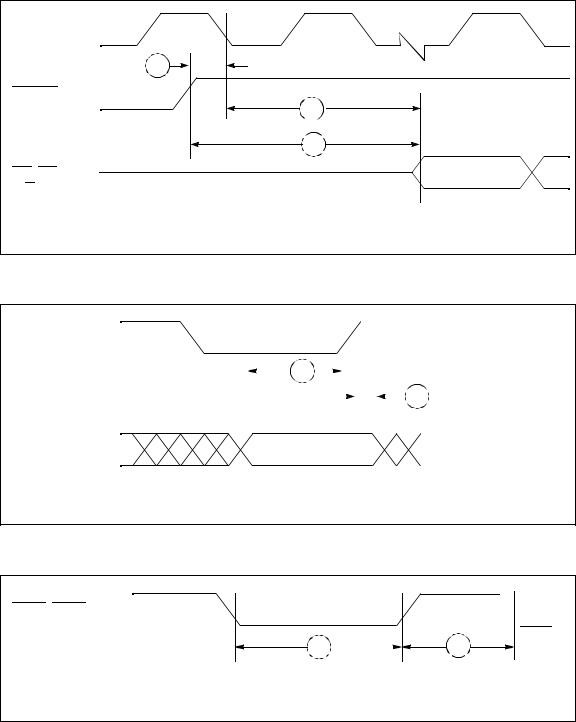
DSP56001 Electrical Characteristics
EXTAL |
12 |
RESET |
13 |
11 |
A0-A15, |
DS, PS |
X/Y |
Control Figure 2. Synchronous Reset Timing |
|
|
|
|
|
|
|
|
|
|
|
|
|
|
|
|
|
VIHR |
||
|
|
|
|
|
|
|
|
|
|
|
|
|
|
|
|
|
|||
RESET |
|
|
|
|
|
|
|
|
|
|
|
|
|
|
|
|
|
|
|
|
|
|
|
14 |
|
|
|
|
|
|
|
|
|
|
15 |
|
|
|
|
|
|
|
|
|
|
|
|
|
|||||||||||
|
|
|
|
|
|
|
|
|
|
|
|
|
|
|
|
|
|||
|
|
|
|
|
|
|
|
|
|
|
|
|
|
|
|
|
|
|
|
|
|
|
|
|
|
|
|
|
|
|
|
|
|
|
|
|
|
|
|
|
|
|
|
|
|
|
|
|
|
|
|
|
|
|
|
|
|
||
|
|
|
|
|
|
|
|
|
|
|
|
|
|
|
|
|
|||
|
|
|
|
|
|
|
|
|
|
|
|
|
|
|
|
|
|
|
|
|
|
|
|
VIHM |
|
|
|
VIH |
|||||||||||
MODA, MODB |
|
|
|
|
|
|
|
|
|
|
|
|
|
|
|
|
|
|
|
|
|
VILM |
|
|
|
|
|
IRQA, |
IRQB |
||||||||||
|
|
|
|
|
|
|
VIL |
||||||||||||
|
|
|
|
|
|
|
|
|
|
|
|
|
|
|
|
|
|
|
|
Control Figure 3. Operating Mode Select Timing
IRQA, IRQB
16 |
|
16a |
|
Control Figure 4. External Interrupt Timing (Negative Edge-Triggered)
MOTOROLA |
DSP56001 |
14 |
|

DSP56001 Electrical Characteristics
A0-A15 |
First Interrupt Instruction Execution |
RD |
|
|
20 |
WR |
|
|
21 |
17 |
19 |
IRQA |
|
IRQB |
|
|
a) First Interrupt Instruction Execution |
General |
|
Purpose |
|
I/O |
|
18 |
22 |
IRQA |
|
IRQB |
|
|
b) General Purpose I/O |
Control Figure 5. External Level-Sensitive Fast Interrupt Timing |
|
DSP56001 |
MOTOROLA |
|
15 |

DSP56001 Electrical Characteristics
EXTAL |
T0, T2 |
T1, T3 |
|
|
|
|
23 |
|
IRQA, IRQB |
|
|
|
|
24 |
A0-A15, DS |
|
|
PS, X/Y |
|
|
Control Figure 6. Synchronous Interrupt and Synchronous Wait State Timing |
||
IRQA |
25 |
|
|
|
|
|
26 |
|
A0-A15, DS, |
|
|
First Instruction Fetch |
||||
|
|
|
|
|
|
||
PS, |
X/Y |
|
|
|
|||
|
|
|
|
Control Figure 7. Recovery from Stop State Using |
|
|
|
|
|
|
|
IRQA |
|||
IRQA |
27 |
|
|
|
28 |
A0-A15, DS, |
First IRQA Interrupt |
PS, X/Y |
Instruction Fetch |
Control Figure 8. Recovery from Stop State Using IRQA Interrupt Service |
|
MOTOROLA |
DSP56001 |
16 |
|

DSP56001 Electrical Characteristics
HOST PORT USAGE CONSIDERATIONS
Careful synchronization is required when reading multibit registers that are written by another asynchronous system. This is a common problem when two asynchronous systems are connected. The situation exists in the Host port. The considerations for proper operation are discussed below.
Host Programmer Considerations
1.Unsynchronized Reading of Receive Byte Registers
When reading receive byte registers, RXH, RXM, or RXL, the Host programmer should use interrupts or poll the RXDF flag which indicates that data is available. This assures that the data in the receive byte registers will be stable.
2.Overwriting Transmit Byte Registers
The Host programmer should not write to the transmit byte registers, TXH, TXM, or TXL, unless the TXDE bit is set indicating that the transmit byte registers are empty. This guarantees that the transmit byte registers will transfer valid data to the HRX register.
3.Synchronization of Status Bits from DSP to Host
HC, HREQ, DMA, HF3, HF2, TRDY, TXDE, and RXDF (refer to DSP56000/DSP56001 User’s Manual, I/O Interface section, Host/ DMA Interface Programming Model for descriptions of these status bits) status bits are set or cleared from inside the DSP and read by the Host processor. The Host can read these status bits very quickly without regard to the clock rate used by the DSP, but the possibility exists that the state of the bit could be changing during the read operation. This is generally not a system problem, since the bit will be read correctly in the next pass of any Host polling routine.
However, if the Host asserts the HEN for more than timing number 31a (T31a), with a minimum cycle time of timing number 32a (T32a), then the status is guaranteed to be stable.
A potential problem exists when reading status bits HF3 and HF2 as an encoded pair. If the DSP changes HF3 and HF2 from 00 to 11, there is a small probability that the Host could read the bits during the transition and receive 01 or 10 instead of 11. If the combination of HF3 and HF2 has significance, the Host could read the wrong combination.
Solution:
a.Read the bits twice and check for consensus.
b.Assert HEN access for T31a so that status bit transitions are stabilized.
4.Overwriting the Host Vector
The Host programmer should change the Host Vector register only when the Host Command bit (HC) is clear. This change will guarantee that the DSP interrupt control logic will receive a stable vector.
5.Cancelling a Pending Host Command Exception
The Host processor may elect to clear the HC bit to cancel the Host Command Exception request at any time before it is recognized by the DSP. Because the Host does not know exactly when the exception will be recognized (due to exception processing synchronization and pipeline delays), the DSP may execute the Host exception after the HC bit is cleared. For these reasons, the HV bits must not be changed at the same time the HC bit is cleared.
DSP Programmer Considerations
1.Reading HF0 and HF1 as an Encoded Pair
DMA, HF1, HF0, and HCP, HTDE, and HRDF (refer to DSP56000/DSP56001 User’s Manual, I/O Interface section, Host/DMA Interface Programming Model for descriptions of these status bits) status bits are set or cleared by the Host processor side of the interface. These bits are individually synchronized to the DSP clock.
A potential problem exists when reading status bits HF1 and HF2 as an encoded pair, i.e., the four combinations 00, 01, 10, and 11 each have significance. A very small probability exists that the DSP will read the status bits synchronized during transition. The solution to this potential problem is to read the bits twice for consensus.
DSP56001 |
MOTOROLA |
|
17 |

DSP56001 Electrical Characteristics
AC Electrical Characteristics - Host I/O Timing
(Vcc = 5.0 Vdc + 10%, TJ = -40 to +105° C, CL = 50 pf + 1 TTL Load at 20.5 MHz and 27 MHz) (Vcc = 5.0 Vdc + 5%, TJ = -40 to +105° C, CL = 50 pf + 1 TTL Load at 33 MHz)
(see Host Figures 1 through 6)
cyc = Clock cycle = 1/2 instruction cycle = 2 T cycles tHSDL = Host Synchronization Delay Time
Active low lines should be “pulled up” in a manner consistent with the AC and DC specifications
Num |
|
|
|
|
|
|
|
Characteristics |
20.5 MHz |
27 MHz |
33 MHz |
Unit |
||||||||||||||||||||||||||
|
|
|
|
|
|
|
|
|
|
|
|
|
|
|
|
|
|
|
|
|
|
|
|
|
|
|
|
|
Min |
|
Max |
Min |
|
Max |
Min |
|
Max |
|
|
|
|
|
|
|
|
|
|
|
|
|
|
|
|
|
|
|
|
|
|
|
|
|
|
|
|
|
|
|
|
|
|
||||||
|
|
|
|
|
|
|
|
|
|
|
|
|
||||||||||||||||||||||||||
30 |
|
Host Synchronous Delay (see Note 1) |
tcl |
|
cyc+tcl |
tcl |
|
cyc+tcl |
tcl |
|
cyc+tcl |
ns |
||||||||||||||||||||||||||
|
|
|
|
|
|
|
|
|
|
|
|
|
|
|
|
|
|
|
|
|
|
|
|
|
|
|
|
|
|
|
|
|
|
|
|
|
||
31 |
|
|
|
|
|
|
|
|
|
|
|
|
|
|
|
|
|
|
|
|
|
|
|
|
|
|
|
|
|
|
|
|
|
|
|
|
|
|
HEN/HACK Assertion Width |
|
|
|
|
|
|
|
|
|
|
||||||||||||||||||||||||||||
|
|
|
|
|
|
|
|
|
|
(see Note 2) |
|
|
|
|
|
|
|
|
|
|
||||||||||||||||||
|
|
|
a.CVR, ICR, ISR Read (see Note 4) |
cyc+60 |
|
— |
cyc+46 |
|
— |
cyc+37 |
|
— |
ns |
|||||||||||||||||||||||||
|
|
|
b.Read |
|
|
|
|
|
|
|
|
|
|
|
|
|
|
|
|
|
|
|
50 |
|
— |
39 |
|
— |
31 |
|
— |
ns |
||||||
|
|
|
c.Write |
|
|
|
|
|
|
|
|
|
|
|
|
|
|
|
|
|
|
|
25 |
|
— |
19 |
|
— |
16 |
|
— |
ns |
||||||
|
|
|
|
|
|
|
|
|
|
|
|
|
|
|
|
|
|
|
|
|
|
|
|
|
|
|
|
|
|
|
|
|
|
|
|
|||
32 |
|
|
|
|
|
|
|
|
|
|
|
|
|
|
|
|
|
|
|
|
|
|
|
|
|
|
|
|
25 |
|
— |
19 |
|
— |
16 |
|
— |
ns |
|
HEN/HACK Deassertion Width |
|||||||||||||||||||||||||||||||||||||
|
|
|
|
|
|
|
|
|
(see Note 2 and 5) |
|
|
|
|
|
|
|
|
|
|
|||||||||||||||||||
|
|
|
|
|
|
|
|
|
|
|
|
|
|
|||||||||||||||||||||||||
32a |
|
|
Minimum Cycle Time Between Two |
|
|
|
|
|
|
|
|
|
|
|||||||||||||||||||||||||
|
|
|
HEN Assertion for Consecutive CVR, |
2*cyc+60 |
|
— |
2 *cyc+46 |
|
— |
2 *cyc+37 |
|
— |
ns |
|||||||||||||||||||||||||
|
|
|
ICR, and ISR Reads |
(see Note 2) |
|
|
|
|
|
|
|
|
|
|
||||||||||||||||||||||||
|
|
|
|
|
|
|
|
|
|
|
|
|
|
|||||||||||||||||||||||||
33 |
|
|
Host Data Input Setup Time Before |
5 |
|
— |
4 |
|
— |
4 |
|
— |
ns |
|||||||||||||||||||||||||
|
|
|
HEN/HACK Deassertion |
|
|
|
|
|
|
|
|
|
|
|||||||||||||||||||||||||
|
|
|
|
|
|
|
|
|
|
|
|
|
|
|
|
|
|
|
|
|||||||||||||||||||
34 |
|
|
Host Data Input Hold Time After |
|
|
|
|
|
|
5 |
|
— |
4 |
|
— |
4 |
|
— |
ns |
|||||||||||||||||||
|
HEN/ |
|||||||||||||||||||||||||||||||||||||
|
|
|
HACK Deassertion |
|
|
|
|
|
|
|
|
|
|
|
|
|
|
|
|
|
|
|
|
|
|
|
|
|
|
|
|
|
||||||
|
|
|
|
|
|
|
|
|
|
|
|
|
|
|
|
|
|
|
|
|
|
|
|
|
|
|
|
|
|
|
|
|
|
|||||
35 |
|
|
|
|
|
|
|
|
|
|
|
|
|
|
|
|
|
|
|
|
|
|
|
|
|
|
|
|
0 |
|
— |
0 |
|
— |
0 |
|
— |
ns |
HEN/HACK Assertion to Output Data |
||||||||||||||||||||||||||||||||||||||
|
|
|
Active from High Impedance |
|
|
|
|
|
|
|
|
|
|
|||||||||||||||||||||||||
|
|
|
|
|
|
|
|
|
|
|
|
|
|
|
|
|
|
|
|
|
|
|
|
|
|
|
|
|
|
|
|
|
|
|||||
36 |
|
|
|
|
|
|
|
|
|
|
|
|
|
|
|
|
|
|
|
|
|
|
|
|
|
|
|
|
— |
|
50 |
— |
|
39 |
— |
|
31 |
ns |
HEN/HACK Assertion to Output Data |
||||||||||||||||||||||||||||||||||||||
|
|
|
Valid (periodically sampled, and not |
|
|
|
|
|
|
|
|
|
|
|||||||||||||||||||||||||
|
|
|
100% tested) |
|
|
|
|
|
|
|
|
|
|
|
|
|
|
|
|
|
|
|
|
|
|
|
|
|
|
|
|
|
||||||
|
|
|
|
|
|
|
|
|
|
|
|
|
|
|
|
|
|
|
|
|
|
|
|
|
|
|
|
|
|
|
|
|
|
|||||
37 |
|
|
|
|
|
|
|
|
|
|
|
|
|
|
|
|
|
|
|
|
|
|
|
|
|
|
|
|
— |
|
35 |
— |
|
27 |
— |
|
22 |
ns |
|
HEN/HACK Deassertion to Output |
|||||||||||||||||||||||||||||||||||||
|
|
|
Data High Impedance |
|
|
|
|
|
|
|
|
|
|
|
|
|
|
|
|
|
|
|
|
|
|
|
|
|
|
|
|
|
||||||
|
|
|
|
|
|
|
|
|
|
|
|
|
|
|
|
|
|
|
|
|
|
|
|
|
||||||||||||||
38 |
|
|
Output Data Hold Time After |
|
|
|
|
|
|
|
|
|
|
|
|
5 |
|
— |
4 |
|
— |
4 |
|
— |
ns |
|||||||||||||
|
HEN/ |
|||||||||||||||||||||||||||||||||||||
|
|
|
HACK Deassertion |
|
|
|
|
|
|
|
|
|
|
|
|
|
|
|
|
|
|
|
|
|
|
|
|
|
|
|
|
|
||||||
|
|
|
|
|
|
|
|
|
|
|
|
|
|
|
|
|
|
|
|
|
|
|
|
|||||||||||||||
39 |
|
|
|
|
|
|
|
Low Setup Time Before |
|
|
|
|
|
|
|
|
|
|
0 |
|
— |
0 |
|
— |
0 |
|
— |
ns |
||||||||||
|
HR/W |
HEN |
||||||||||||||||||||||||||||||||||||
|
|
|
Assertion |
|
|
|
|
|
|
|
|
|
|
|
|
|
|
|
|
|
|
|
|
|
|
|
|
|
|
|
|
|
||||||
|
|
|
|
|
|
|
|
|
|
|
|
|
|
|
|
|
|
|
|
|
|
|
|
|
||||||||||||||
40 |
|
|
|
|
|
|
|
Low Hold Time After |
|
|
|
|
|
|
|
|
|
|
|
5 |
|
— |
4 |
|
— |
4 |
|
— |
ns |
|||||||||
|
HR/W |
HEN |
||||||||||||||||||||||||||||||||||||
|
|
|
Deassertion |
|
|
|
|
|
|
|
|
|
|
|
|
|
|
|
|
|
|
|
|
|
|
|
|
|
|
|
|
|
||||||
|
|
|
|
|
|
|
|
|
|
|
|
|
|
|
|
|
|
|
|
|
|
|
|
|||||||||||||||
41 |
|
|
|
|
|
|
|
High Setup Time to |
|
|
|
|
|
|
|
|
|
|
|
0 |
|
— |
0 |
|
— |
0 |
|
— |
ns |
|||||||||
|
HR/W |
HEN |
||||||||||||||||||||||||||||||||||||
|
|
|
Assertion |
|
|
|
|
|
|
|
|
|
|
|
|
|
|
|
|
|
|
|
|
|
|
|
|
|
|
|
|
|
||||||
|
|
|
|
|
|
|
|
|
|
|
|
|
|
|
|
|
|
|
|
|
|
|||||||||||||||||
42 |
|
|
|
|
|
|
|
High Hold Time After |
|
|
|
|
|
|
|
|
|
|
|
5 |
|
— |
4 |
|
— |
4 |
|
— |
ns |
|||||||||
|
HR/W |
HEN/ |
||||||||||||||||||||||||||||||||||||
|
|
|
HACK Deassertion |
|
|
|
|
|
|
|
|
|
|
|
|
|
|
|
|
|
|
|
|
|
|
|
|
|
|
|
|
|
||||||
|
|
|
|
|
|
|
|
|
|
|
|
|
|
|
|
|
||||||||||||||||||||||
43 |
|
HA0-HA2 Setup Time Before |
|
|
|
|
|
|
|
|
|
|
0 |
|
— |
0 |
|
— |
0 |
|
— |
ns |
||||||||||||||||
HEN |
||||||||||||||||||||||||||||||||||||||
|
|
|
Assertion |
|
|
|
|
|
|
|
|
|
|
|
|
|
|
|
|
|
|
|
|
|
|
|
|
|
|
|
|
|
||||||
|
|
|
|
|
|
|
|
|
|
|
|
|
|
|
|
|
||||||||||||||||||||||
44 |
|
|
HA0-HA2 Hold Time After |
|
|
|
|
|
|
|
|
|
5 |
|
— |
4 |
|
— |
4 |
|
— |
ns |
||||||||||||||||
|
HEN |
|||||||||||||||||||||||||||||||||||||
|
|
|
Deassertion |
|
|
|
|
|
|
|
|
|
|
|
|
|
|
|
|
|
|
|
|
|
|
|
|
|
|
|
|
|
||||||
|
|
|
|
|
|
|
|
|
|
|
|
|
|
|
|
|
||||||||||||||||||||||
45 |
|
DMA |
|
|
Assertion to |
|
|
|
|
|
|
|
|
|
|
|
5 |
|
60 |
4 |
|
46 |
4 |
|
49 |
ns |
||||||||||||
HACK |
HREQ |
|||||||||||||||||||||||||||||||||||||
|
|
|
Deassertion |
(see Note 3) |
|
|
|
|
|
|
|
|
|
|
||||||||||||||||||||||||
|
|
|
|
|
|
|
|
|
|
|
|
|
|
|
|
|
|
|
|
|
|
|
|
|
|
|
|
|
|
|
|
|
|
|
|
|
|
|
MOTOROLA |
DSP56001 |
18 |
|

DSP56001 Electrical Characteristics
AC Electrical Characteristics - Host I/O Timing (Continued)
(Vcc = 5.0 Vdc + 10%, TJ = -40 to +105° C, CL = 50 pf + 1 TTL Load at 20.5 MHz and 27 MHz (Vcc = 5.0 Vdc + 5%, TJ = -40 to +105° C, CL = 50 pf + 1 TTL Load at 33 MHz,
see Host Figures 1 through 6)
cyc = Clock cycle = 1/2 instruction cycle = 2 T cycles tHSDL = Host Synchronization Delay Time
Active low lines should be “pulled up” in a manner consistent with the AC and DC specifications
Num |
|
Characteristics |
20.5 MHz |
27 MHz |
|
|
33 MHz |
Unit |
||||||||||||||||||
|
|
|
|
|
|
|
|
|
|
|
|
|
|
|
|
Min |
|
Max |
Min |
|
Max |
|
Min |
|
Max |
|
|
|
|
|
|
|
|
|
|
|
|
|
|
|
|
|
|
|
|
|
|
||||||
|
|
|
|
|
|
|
|
|
|
|
|
|
|
|
|
|
|
|
|
|
|
|
|
|||
46 |
DMA |
|
|
|
|
Deassertion to |
|
|
|
|
|
|
|
|
|
|
|
|
|
|
|
|
|
|||
HACK |
HREQ |
|
|
|
|
|
|
|
|
|
|
|
||||||||||||||
|
Assertion |
(see Note 3) |
|
|
|
|
|
|
|
|
|
|
|
|||||||||||||
|
|
|
|
|
|
|
|
for DMA RXL Read |
tHSDL+cyc |
|
— |
tHSDL+cyc |
|
— |
|
tHSDL+cyc |
|
— |
ns |
|||||||
|
|
|
|
|
|
|
|
|
|
|
|
|
|
|
|
+tch+5 |
|
|
+tch+4 |
|
|
|
+tch+4 |
|
|
|
|
|
|
|
|
|
|
|
for DMA TXL Write |
tHSDL+cyc+5 |
|
— |
tHSDL+cyc+4 |
|
— |
|
tHSDL+cyc+4 |
|
— |
ns |
|||||||
|
|
|
|
|
|
|
|
for All Other Cases |
5 |
|
— |
4 |
|
— |
|
4 |
|
— |
ns |
|||||||
|
|
|
|
|
|
|
|
|
|
|
|
|
|
|
|
|
|
|
|
|||||||
47 |
Delay from |
|
|
|
|
Deassertion to |
|
|
|
|
tHSDL+cyc |
|
— |
tHSDL+cyc |
|
— |
|
tHSDL+cyc |
|
— |
ns |
|||||
HEN |
HREQ |
|||||||||||||||||||||||||
|
Assertion for RXL Read |
(see Note 3) |
+tch+5 |
|
|
+tch+4 |
|
|
|
+tch+4 |
|
|
|
|||||||||||||
|
|
|
|
|
|
|
|
|
|
|
|
|
|
|
|
|
|
|
|
|||||||
48 |
Delay from |
|
|
|
|
|
Deassertion to |
|
|
|
|
tHSDL+cyc+5 |
|
— |
tHSDL+cyc+4 |
|
— |
|
tHSDL+cyc+4 |
|
— |
ns |
||||
HEN |
HREQ |
|||||||||||||||||||||||||
|
Assertion for TXL Write |
(see Note 3) |
|
|
|
|
|
|
|
|
|
|
|
|||||||||||||
|
|
|
|
|
|
|
|
|
|
|
|
|
|
|
|
|
||||||||||
49 |
Delay from |
|
|
|
Assertion to |
|
|
|
|
|
|
|
|
|
|
|
|
|
|
|
||||||
HEN |
HREQ |
|
|
|
|
|
|
|
|
|
|
|
||||||||||||||
|
DeassertionforRXLRead,TXLWrite |
5 |
|
75 |
4 |
|
70 |
|
4 |
|
65 |
ns |
||||||||||||||
|
(see Note 3) |
|
|
|
|
|
|
|
|
|
|
|
|
|
|
|
|
|
|
|||||||
|
|
|
|
|
|
|
|
|
|
|
|
|
|
|
|
|
|
|
|
|
|
|
|
|
|
|
Notes:
1. “Host synchronization delay (tHSDL)” is the time period required for the DSP56001 to sample any external asynchronous input signal, determine whether it is high or low, and synchronize it to the DSP56001 internal clock.
2.See HOST PORT USAGE CONSIDERATIONS.
3.HREQ is pulled up by a 1kΩ resistor.
4.This timing must be adhered to only if two consecutive reads from one of these registers are executed.
5.It is recommended that timing #32 be 2cyc+tch+10 minimum for 20.5 MHz, 2cyc+tch+7 minimum for 27 MHz, and 2cyc+tch+6 minimum for 33 MHz if two consecutive writes to TXL are executed without polling TXDE or HREQ.
EXTERNAL
30 |
30 |
INTERNAL
Host Figure 1. Host Synchronization Delay
DSP56001 |
MOTOROLA |
|
19 |

DSP56001 Electrical Characteristics
HREQ |
|
|
|
(OUTPUT) |
|
|
|
|
31 |
32 |
|
HACK |
|
|
|
(INPUT) |
|
|
|
|
41 |
42 |
|
HR/W |
|
|
|
(INPUT) |
|
|
|
|
36 |
37 |
|
|
35 |
38 |
|
H0-H7 |
Data |
Valid |
|
(OUTPUT) |
|||
|
|
||
|
Host Figure 2. Host Interrupt Vector Register (IVR) Read |
||
MOTOROLA |
DSP56001 |
20 |
|
 Loading...