


 Loading...
Mitsubishi M38504M6-XXXSP, M38504M6-XXXFP, M38504E6SS, M38504E6SP, M38504E6FP Datasheet
...MITSUBISHI MICROCOMPUTERS
3850 Group
SINGLE-CHIP 8-BIT CMOS MICROCOMPUTER
DESCRIPTION
The 3850 group is the 8-bit microcomputer based on the 740 family core technology.
The 3850 group is designed for the household products and office automation equipment and includes serial I/O functions, 8-bit timer, and A-D converter.
FEATURES |
|
|
●Basic machine-language instructions |
...................................... 71 |
|
●Minimum instruction execution time .................................. |
0.5 μs |
|
(at 8 MHz oscillation frequency) |
|
|
●Memory size |
|
|
ROM ................................................................... |
|
8K to 24K bytes |
RAM ..................................................................... |
|
512 to 640 byte |
●Programmable input/output ports ............................................ |
34 |
|
●Interrupts ................................................. |
|
14 sources, 14 vectors |
●Timers ............................................................................. |
|
8 - bit 4 |
●Serial I/O ....................... |
8-bit 1(UART or Clock-synchronized) |
|
●PWM ............................................................................... |
|
8 - bit 1 |
●A-D converter ............................................... |
|
10 - bit 5 channels |
●Watchdog timer ............................................................ |
|
16 - bit 1 |
●Clock generating circuit ..................................... |
|
Built - in 2 circuits |
(connect to external ceramic resonator or quartz-crystal oscillator) |
||
●Power source voltage |
|
In high-speed mode .................................................. |
4.0 to 5.5 V |
(at 8 MHz oscillation frequency) |
|
In high-speed mode .................................................. |
2.7 to 5.5 V |
(at 4 MHz oscillation frequency) |
|
In middle-speed mode ............................................... |
2.7 to 5.5 V |
(at 8 MHz oscillation frequency) |
|
In low-speed mode .................................................... |
2.7 to 5.5 V |
(at 32 kHz oscillation frequency) |
|
●Power dissipation |
|
In high-speed mode .......................................................... |
34 mW |
(at 8 MHz oscillation frequency, at 5 V power source voltage) |
|
In low-speed mode ............................................................ |
60 μW |
(at 32 kHz oscillation frequency, at 3 V power source voltage) |
|
●Operating temperature range.................................... |
–20 to 85°C |
APPLICATION
Office automation equipment, FA equipment, Household products, Consumer electronics, etc.
PIN CONFIGURATION (TOP VIEW)
VCC 1
VREF 
 2
2
AVSS |
|
|
3 |
|
P44/INT3/PWM 

 4
4
P43/INT2 

 5
5
P42/INT1 

 6
6
P41/INT0 

 7
7
P40/CNTR1 

 8
8
P27/CNTR0/SRDY 

 9
9
P26/SCLK 

 10
10
P25/TxD 

 11
11
P24/RxD 

 12
12
P23 

 13
13
P22 

 14
14
CNVSS 
 15
15
P21/XCIN 

 16
16
P20/XCOUT 

 17
17
RESET 
 18
18
XIN 
 19
19
XOUT 
 20
20
VSS 
 21
21
XXXSP-M38503M4 |
XXXFP-M38503M4 |
|
|
|
P30/AN0 |
42 |
|
|
|
|
|
|
P31/AN1 |
41 |
|
|
|
|
|||
|
|
|
P32/AN2 |
40 |
|
|
|
|
|||
|
|
|
P33/AN3 |
39 |
|
|
|
|
|
|
P34/AN4 |
38 |
|
|
|
|
|||
|
|
|
P00 |
37 |
|
|
|
|
|
|
P01 |
36 |
|
|
|
|
|||
|
|
|
P02 |
35 |
|
|
|
|
|
|
P03 |
34 |
|
|
|
|
|||
|
|
|
P04 |
33 |
|
|
|
|
|||
|
|
|
P05 |
32 |
|
|
|
|
|||
|
|
|
P06 |
31 |
|
|
|
|
|
|
P07 |
30 |
|
|
|
|
|
|
P10 |
29 |
|
|
|
|
|
|
P11 |
28 |
|
|
|
|
|
|
P12 |
27 |
|
|
|
|
|
|
P13/(LED0) |
26 |
|
|
|
|
|
|
P14/(LED1) |
25 |
|
|
|
|
|
|
P15/(LED2) |
24 |
|
|
|
|
|||
|
|
|
P16/(LED3) |
23 |
|
|
|
|
|||
|
|
|
P17/(LED4) |
22 |
|
|
|
|
|||
|
|
|
|
Package type : |
FP ........................... |
42P2R-A (42-pin plastic-molded SSOP) |
Package type : |
SP ........................... |
42P4B (42-pin shrink plastic-molded DIP) |
Fig. 1 M38503M4-XXXFP/SP pin configuration

2 |
diagramblockFunctional 2 .Fig |
19 |
20 |
|
|
|
|
|
|
21 |
1 |
18 |
|
15 |
|
|
|
|
BLOCKFUNCTIONAL |
|
|
|
|
FUNCTIONAL BLOCK DIAGRAM |
|
|
|
|
|
|
|
|
|
|
|
|
|
|
|
|
|||
|
|
Main-clock |
Main-clock |
|
|
|
|
|
|
|
Reset input |
|
|
|
|
|
|
|
|
|
|
|
|
input |
output |
|
|
|
|
|
|
|
|
|
|
|
|
|
|
|
|
|
|
|
|
|
|
|
|
|
|
|
|
|
CNVSS |
|
|
|
|
|
|
|
|||
|
|
XIN |
XOUT |
|
|
|
|
|
|
VSS |
VCC |
RESET |
|
|
|
|
|
|
|
||
|
|
|
Sub-clock Sub-clock |
|
|
|
|
|
|
|
|
|
|
|
|
|
|
|
|
||
|
|
|
|
input |
output |
|
|
|
|
|
|
|
|
|
|
|
|
|
|
|
|
|
|
|
|
XCIN |
XCOUT |
|
|
|
|
|
|
|
|
|
|
|
|
|
|
|
|
|
|
|
Clock generating circuit |
|
|
|
|
|
|
|
|
|
|
Timer |
1( 8 ) |
|
|
|
|||
|
|
|
|
|
|
|
|
|
|
|
|
|
|
|
|
|
|
|
|||
|
|
|
|
|
|
|
|
|
|
|
|
|
|
Prescaler |
12(8) |
Timer |
2( 8 ) |
|
|
|
|
|
|
|
|
|
|
|
|
|
|
|
|
|
|
Prescaler |
X(8) |
Timer |
X( 8 ) |
|
|
|
|
|
|
Watchdog |
|
|
|
|
|
|
|
|
|
|
Prescaler |
Y(8) |
Timer |
Y( 8 ) |
|
|
|
||
|
|
|
Reset |
|
|
|
|
|
|
|
|
|
|
|
|
|
|
|
|
||
|
|
|
timer |
|
|
|
|
|
|
|
|
|
|
|
|
|
|
|
|
|
|
|
|
|
|
|
|
|
|
|
|
|
|
|
|
|
|
|
|
|
|
|
|
|
|
|
|
A-D |
PWM |
|
|
|
|
|
SI/O(8) |
|
|
|
|
|
|
|
SINGLE |
|
|
|
|
|
|
|
|
|
|
|
|
|
|
|
|
|
|
- |
|
|
|||
|
|
|
converter |
(8) |
|
|
|
|
|
|
|
|
|
|
|
|
|
|
|
||
|
|
|
|
|
|
|
|
|
|
|
|
|
|
|
|
MICROCOMPUTERCMOSBIT-8CHIP |
Group3850 |
MICROCOMPUTERSMITSUBISHI |
|||
|
|
|
|
(10) |
|
|
|
|
|
|
|
|
|
|
|
|
|
|
|||
|
|
|
|
|
|
|
|
|
|
|
|
|
|
|
XCOUT |
|
|
|
|
|
|
|
|
|
|
|
|
|
|
|
|
|
|
|
|
|
XCIN |
|
|
|
|
|
|
|
|
|
|
|
|
|
|
|
|
INT0– |
|
|
|
|
|
|
|
|
|
|
|
|
|
|
|
|
|
|
|
|
|
INT3 |
|
|
|
|
|
|
|
|
|
|
|
|
|
|
|
|
|
P4(5) |
|
P3(5) |
|
|
|
P2(8) |
|
P1(8) |
|
P0(8) |
|
|
|
||
|
|
|
2 |
3 |
4 |
5 |
6 |
7 |
8 |
38 39 40 41 42 |
|
|
9 |
10 11 12 13 1416 17 |
22 23 24 25 26 27 28 29 |
30 31 32 33 34 35 36 37 |
|
|
|
||
|
|
|
|
|
I/O port P4 |
I/O port P3 |
|
|
|
I/O port P2 |
I/O port P1 |
I/O port P0 |
|
|
|
||||||
|
|
|
VREF |
|
|
|
|
|
|
|
|
|
|
|
|
|
|
|
|
|
|
|
|
|
AVSS |
|
|
|
|
|
|
|
|
|
|
|
|
|
|
|
|
|
|

MITSUBISHI MICROCOMPUTERS
3850 Group
SINGLE-CHIP 8-BIT CMOS MICROCOMPUTER
PIN DESCRIPTION
Table 1 Pin description
|
|
Pin |
Name |
Functions |
|
|
|
|
Function except a port function |
||||
|
|
|
|
|
|
|
|
|
|
|
|
|
|
|
VCC, VSS |
Power source |
•Apply voltage of 2.7 V – 5.5 V to Vcc, and 0 V to Vss. |
|
||
|
|
|
|
|
|
|
|
CNVSS |
CNVSS input |
•This pin controls the operation mode of the chip. |
|
||
|
•Normally connected to VSS. |
|
||||
|
|
|
|
|
|
|
|
|
|
|
|
|
|
|
|
|
Reset input |
•Reset input pin for active “L.” |
|
|
|
RESET |
|
||||
|
XIN |
|
|
Clock input |
•Input and output pins for the clock generating circuit. |
|
|
|
|
•Connect a ceramic resonator or quartz-crystal oscillator between the XIN and XOUT pins to set |
|||
|
|
|
|
|
||
|
|
|
|
|
the oscillation frequency. |
|
|
|
|
|
|
|
|
|
XOUT |
Clock output |
•When an external clock is used, connect the clock source to the XIN pin and leave the XOUT |
|||
|
|
|
|
|
pin open. |
|
|
|
|
|
|
•8-bit CMOS I/O port. |
|
|
P00 |
–P07 |
I/O port P0 |
•I/O direction register allows each pin to be individually programmed as either input or output. |
||
|
|
|
|
|
||
|
|
|
|
|
•CMOS compatible input level. |
|
|
|
|
|
|
|
|
|
P10 |
–P17 |
I/O port P1 |
•CMOS 3-state output structure. |
|
|
|
•P13 to P17 (5 bits) are enabled to output large current for LED drive. |
|||||
|
|
|
|
|
||
|
|
|
|
|
|
|
|
P20 |
/XCOUT |
|
•8-bit CMOS I/O port. |
• Sub-clock generating circuit I/O |
|
|
P21 |
/XCIN |
|
•I/O direction register allows each pin to be individually |
pins (connect a resonator) |
|
|
|
|
|
|
programmed as either input or output. |
|
|
P22 |
|
|
|
|
|
|
|
|
|
•CMOS compatible input level. |
|
|
|
P23 |
|
|
|
|
|
|
|
|
|
•P20, P21, P24 to P27: CMOS3-state output structure. |
|
|
|
|
|
|
|
|
|
|
P24 |
/RxD |
I/O port P2 |
• Serial I/O function pin |
||
|
•P22, P23: N-channel open-drain structure. |
|||||
|
P25 |
/TxD |
|
|||
|
|
|
|
|||
|
|
|
|
|
||
|
P26/SCLK |
|
|
|
||
|
|
|
|
|
|
|
|
P27 |
/CNTR0/ |
|
|
• Serial I/O function pin/ |
|
|
SRDY |
|
|
Timer X function pin |
||
|
|
|
|
|
|
|
|
P30/AN0– |
I/O port P3 |
•8-bit CMOS I/O port with the same function as port P0. |
• A-D converter input pin |
||
|
P34 |
/AN4 |
|
•CMOS compatible input level. |
|
|
|
|
|
|
|
•CMOS 3-state output structure. |
|
|
|
|
|
|
|
|
|
P40 |
/CNTR1 |
I/O port P4 |
•8-bit CMOS I/O port with the same function as port P0. |
• Timer Y function pin |
|
|
P41 |
/INT0– |
|
•CMOS compatible input level. |
• Interrupt input pins |
|
|
P43/INT2 |
|
•CMOS 3-state output structure. |
|
||
|
P44 |
/INT3/PWM |
|
|
• Interrupt input pin |
|
|
|
|
• PWM output pin |
|||
|
|
|
|
|
|
|
|
|
|
|
|
|
|
3

MITSUBISHI MICROCOMPUTERS
3850 Group
SINGLE-CHIP 8-BIT CMOS MICROCOMPUTER
PART NUMBERING
Product M3850 3 M 4 XXX FP
Package type
FP |
: 42P2R-A package |
SP |
: 42P4B package |
SS |
: 42S1B-A package |
ROM number
Omitted in some types.
ROM/PROM size
1 : 4096 bytes
2 : 8192 bytes
3 : 12288 bytes
4 : 16384 bytes
5 : 20480 bytes
6 : 24576 bytes
7 : 28672 bytes
8 : 32768 bytes
9 : 36864 bytes A : 40960 bytes B : 45056 bytes C : 49152 bytes D : 53248 bytes E : 57344 bytes F : 61440 bytes
The first 128 bytes and the last 2 bytes of ROM are reserved areas ; they cannot be used.
Memory type
M : Mask ROM version
E : EPROM or One Time PROM version
RAM size
0 : 192 bytes
1 : 256 bytes
2 : 384 bytes
3 : 512 bytes
4 : 640 bytes
5 : 768 bytes
6 : 896 bytes
7 : 1024 bytes
8 : 1536 bytes
9 : 2048 bytes
Fig. 3 Part numbering
4

MITSUBISHI MICROCOMPUTERS
3850 Group
SINGLE-CHIP 8-BIT CMOS MICROCOMPUTER
GROUP EXPANSION |
Packages |
Mitsubishi plans to expand the 3850 group as follows:
Memory Type
Support for mask ROM, One Time PROM, and EPROM versions.
Memory Size
42P4B.......................................... |
42-pin shrink plastic molded DIP |
42P2R-A ............................................ |
42-pin plastic molded SSOP |
42S1B-A ................... |
42-pin shrink ceramic DIP(EPROM version) |
ROM/PROM size ................................................... |
8K to 24K bytes |
RAM size .............................................................. |
512 to 640 bytes |
Memory Expansion Plan
ROM size (bytes)
48K |
|
|
|
|
|
|
|
|
32K |
|
|
|
|
|
|
|
|
28K |
|
|
|
Under development |
|
|
|
|
|
|
|
|
|
|
|
||
24K |
|
|
|
|
M38504M6/E6 |
|
|
|
20K |
|
|
Mass production |
|
|
|
|
|
|
|
|
|
|
|
|
||
16K |
|
|
|
M38503M4/E4 |
|
|
|
|
12K |
|
|
Mass production |
|
|
|
|
|
|
|
|
|
|
|
|
||
8K |
|
|
|
M38503M2 |
|
|
|
|
128 |
192 |
256 |
384 |
512 |
640 |
768 |
896 |
1024 |
RAM size (bytes)
Products under development or planning : the development schedule and specification may be revised without notice.
Planning products may be stopped the development.
Fig. 4 Memory expansion plan
Currently planning products are listed below.
Table 2 Support products |
|
|
|
|
|
|
As of August 1998 |
|
|
|
|
|
|
|
|
||
Product name |
(P) ROM size (bytes) |
RAM size (bytes) |
|
Package |
Remarks |
|||
ROM size for User in ( |
) |
|
||||||
|
|
|
|
|
|
|
||
|
|
|
|
|
|
|
||
M38503M2-XXXSP |
8192 |
|
512 |
|
42P4B |
Mask ROM version |
||
M38503M2-XXXFP |
(8062) |
|
|
42P2R-A |
Mask ROM version |
|||
|
|
|
||||||
M38503M4-XXXSP |
|
|
|
|
|
|
|
Mask ROM version |
M38503E4-XXXSP |
|
|
|
|
42P4B |
One Time PROM version |
||
M38503E4SP |
16384 |
|
|
|
|
|
|
One Time PROM version (blank) |
M38503E4SS |
|
512 |
|
42S1B-A |
EPROM version (stock only replaced by M38504E6SS) |
|||
(16254) |
|
|
||||||
M38503M4-XXXFP |
|
|
|
|
|
|
Mask ROM version |
|
|
|
|
|
|
|
|
||
M38503E4-XXXFP |
|
|
|
|
42P2R-A |
One Time PROM version |
||
M38503E4FP |
|
|
|
|
|
|
|
One Time PROM version (blank) |
M38504M6-XXXSP |
|
|
|
|
|
|
|
Mask ROM version |
M38504E6-XXXSP |
|
|
|
|
42P4B |
One Time PROM version |
||
M38504E6SP |
32768 |
|
|
|
|
|
|
One Time PROM version (blank) |
M38504E6SS |
|
640 |
|
42S1B-A |
EPROM version |
|||
(32638) |
|
|
||||||
M38504M6-XXXFP |
|
|
|
|
|
|
Mask ROM version |
|
|
|
|
|
|
|
|
||
M38504E6-XXXFP |
|
|
|
|
42P2R-A |
One Time PROM version |
||
M38504E6FP |
|
|
|
|
|
|
|
One Time PROM version (blank) |
|
|
|
|
|
|
|
|
|
|
|
|
|
|
|
|
|
5 |
|
|
|
|
|
|
|
|
|
|
|
|
|
|
|
|
|
|
|
|
|
|
|
|
|
|
|
MITSUBISHI MICROCOMPUTERS
3850 Group
SINGLE-CHIP 8-BIT CMOS MICROCOMPUTER
FUNCTIONAL DESCRIPTION
CENTRAL PROCESSING UNIT (CPU)
The 3850 group uses the standard 740 Family instruction set. Refer to the table of 740 Family addressing modes and machine instructions or the 740 Family Software Manual for details on the instruction set.
Machine-resident 740 Family instructions are as follows:
The FST and SLW instructions cannot be used.
The STP, WIT, MUL, and DIV instructions can be used.
[CPU Mode Register (CPUM)] 003B16
The CPU mode register contains the stack page selection bit, etc.
The CPU mode register is allocated at address 003B16.
b7 |
b0 |
CPU mode register
(CPUM : address 003B16)
Processor mode bits
b1 |
b0 |
|
0 |
0 |
: Single-chip mode |
0 |
1 |
: |
1 |
0 |
: Not available |
1 |
1 |
: |
Stack page selection bit 0 : 0 page
1 : 1 page
Not used (return “1” when read) (Do not write “0” to this bit.)
Port XC switch bit
0 : I/O port function (stop oscillating)
1 : XCIN–XCOUT oscillating function
Main clock (XIN–XOUT) stop bit 0 : Oscillating
1 : Stopped
Main clock division ratio selection bits b7 b6
0 0 : φ = f(XIN)/2 (high-speed mode)
0 1 : φ = f(XIN)/8 (middle-speed mode) 1 0 : φ = f(XCIN)/2 (low-speed mode) 1 1 : Not available
Fig. 5 Structure of CPU mode register
6

|
|
|
|
|
|
|
|
|
|
|
|
MITSUBISHI MICROCOMPUTERS |
|||
|
|
|
|
|
|
|
|
|
|
|
|
|
3850 Group |
||
|
|
|
|
|
|
|
|
|
|
|
SINGLE-CHIP 8-BIT CMOS MICROCOMPUTER |
||||
|
|
|
|
|
|
|
|
|
|
|
|
|
|
|
|
MEMORY |
|
|
|
|
|
Zero Page |
|
|
|
||||||
Special Function Register (SFR) Area |
Access to this area with only 2 bytes is possible in the zero page |
||||||||||||||
The Special Function Register area in the zero page contains con- |
addressing mode. |
|
|
|
|||||||||||
trol registers such as I/O ports and timers. |
|
|
Special Page |
|
|
|
|||||||||
RAM |
|
|
|
|
|
|
|
|
|||||||
|
|
|
|
|
Access to this area with only 2 bytes is possible in the special |
||||||||||
RAM is used for data storage and for stack area of subroutine |
page addressing mode. |
|
|
|
|||||||||||
calls and interrupts. |
|
|
|
|
|
|
|
|
|
|
|
|
|
|
|
ROM |
|
|
|
|
|
|
|
|
|
|
|
|
|
|
|
The first 128 bytes and the last 2 bytes of ROM are reserved for |
|
|
|
|
|
|
|
|
|
||||||
device testing and the rest is user area for storing programs. |
|
|
|
|
|
|
|
|
|
||||||
Interrupt Vector Area |
|
|
|
|
|
|
|
|
|
|
|
||||
The interrupt vector area contains reset and interrupt vectors. |
|
|
|
|
|
|
|
|
|
||||||
|
|
|
|
|
|
|
|
|
|
|
|
|
|
|
|
|
RAM area |
|
|
|
|
|
|
|
|
|
|
|
|
|
|
|
|
|
|
|
|
|
|
|
|
|
|
|
|
|
|
|
RAM size |
Address |
|
|
|
000016 |
|
|
|
|
|||||
|
|
|
|
|
|
||||||||||
|
(bytes) |
XXXX16 |
|
|
|
SFR area |
|
|
|
||||||
|
|
|
|
|
|
|
|
|
|
|
|
||||
|
|
|
|
|
|
|
|
|
|
|
|
|
|
|
|
|
192 |
00FF16 |
|
|
|
|
|
|
|
|
|
|
|
Zero page |
|
|
256 |
013F16 |
|
|
|
|
004016 |
|
|
|
|
||||
|
|
|
|
|
|
|
|
|
|
|
|
|
|||
|
384 |
01BF16 |
|
|
|
|
010016 |
|
|
|
|
||||
|
|
|
|
|
|
|
|
|
|
|
|
||||
|
512 |
023F16 |
|
|
|
RAM |
|
|
|
|
|||||
|
|
|
|
|
|
|
|
|
|
|
|
||||
|
640 |
02BF16 |
|
|
|
|
|
|
|
|
|
|
|
||
|
|
|
|
|
|
|
|
|
|
|
|
|
|||
|
768 |
033F16 |
|
|
|
|
|
|
|
|
|
|
|
|
|
|
896 |
03BF16 |
|
|
|
|
|
|
|
XXXX16 |
|
|
|
|
|
|
1024 |
043F16 |
|
|
|
|
|
|
|
|
|
|
|
|
|
|
1536 |
063F16 |
|
|
|
|
|
|
|
|
Reserved area |
|
|
|
|
|
2048 |
083F16 |
|
|
|
|
|
|
|
|
|
|
|
|
|
|
3072 |
0C3F16 |
|
|
|
044016 |
|
|
|
|
|||||
|
4032 |
0FFF16 |
|
|
|
|
|
|
|
|
Not used |
|
|
|
|
|
ROM area |
|
|
|
|
|
|
|
|
|
YYYY16 |
Reserved ROM area |
|
|
|
|
|
|
|
|
|
|
|
|
|
|
|
|
|||
|
|
|
|
|
|
|
|
|
|
|
|
|
|
||
|
ROM size |
Address |
|
|
Address |
|
|
|
|
|
|
(128 bytes) |
|
|
|
|
(bytes) |
YYYY16 |
|
|
ZZZZ16 |
|
|
|
|
|
ZZZZ16 |
|
|
|
|
|
|
|
|
|
|
|
|
|
|
|
|
|
|
|
|
|
4096 |
F00016 |
|
|
F08016 |
|
|
|
|
|
|||||
|
|
|
|
|
|
|
|
|
|
|
|
|
|||
|
8192 |
E00016 |
|
|
E08016 |
|
|
|
|
|
|
|
|
|
|
|
12288 |
D00016 |
|
|
D08016 |
|
|
|
|
|
|
|
|
|
|
|
16384 |
C00016 |
|
|
C08016 |
|
ROM |
|
|
|
|
|
|
|
|
|
20480 |
B00016 |
|
|
B08016 |
|
|
|
|
|
|
||||
|
|
|
|
|
|
|
|
|
|
|
|
|
|||
|
24576 |
A00016 |
|
|
A08016 |
|
|
|
|
|
FF0016 |
|
|
|
|
|
|
|
|
|
|
|
|
||||||||
|
28672 |
900016 |
|
|
908016 |
|
|
|
|
|
|
|
|
|
|
|
32768 |
800016 |
|
|
808016 |
|
|
|
|
|
FFDC16 |
|
|
|
|
|
|
|
|
|
|
|
|
|
|||||||
|
36864 |
700016 |
|
|
708016 |
|
|
|
|
|
|
Interrupt vector area |
|
|
Special page |
|
40960 |
600016 |
|
|
608016 |
|
|
|
|
|
|
|
|
|
|
|
|
|
|
|
|
|
|
|
|
|
|
|
|||
|
45056 |
500016 |
|
|
508016 |
|
|
|
|
|
FFFE16 |
|
|
|
|
|
|
|
|
|
|
|
|
|
|||||||
|
49152 |
400016 |
|
|
408016 |
|
|
|
|
|
Reserved ROM area |
|
|
|
|
|
|
|
|
|
|
|
|
FFFF16 |
|
|
|
||||
|
53248 |
300016 |
|
|
308016 |
|
|
|
|
|
|
|
|
|
|
|
|
|
|
|
|
|
|
|
|
|
|
|
|||
|
57344 |
200016 |
|
|
208016 |
|
|
|
|
|
|
|
|
|
|
|
61440 |
100016 |
|
|
108016 |
|
|
|
|
|
|
|
|
|
|
|
|
|
|
|
|
|
|
|
|
|
|
|
|
|
|
Fig. 6 Memory map diagram
7

MITSUBISHI MICROCOMPUTERS
3850 Group
SINGLE-CHIP 8-BIT CMOS MICROCOMPUTER
000016
000116
000216
000316
000416
000516
000616
000716
000816
000916
000A16
000B16
000C16
000D16
000E16
000F16
001016
001116
001216
001316
001416
001516
001616
001716
001816
001916
001A16
001B16
001C16
001D16
001E16
001F16
Port P0 (P0)
Port P0 direction register (P0D)
Port P1 (P1)
Port P1 direction register (P1D)
Port P2 (P2)
Port P2 direction register (P2D)
Port P3 (P3)
Port P3 direction register (P3D)
Port P4 (P4)
Port P4 direction register (P4D)
Reserved
Reserved
Reserved
Transmit/Receive buffer register (TB/RB)
Serial I/O status register (SIOSTS)
Serial I/O control register (SIOCON)
UART control register (UARTCON)
Baud rate generator (BRG)
PWM control register (PWMCON)
PWM prescaler (PREPWM)
PWM register (PWM)
Reserved : Do not write “1” to this address.
002016
002116
002216
002316
002416
002516
002616
002716
002816
002916
002A16
002B16
002C16
002D16
002E16
002F16
003016
003116
003216
003316
003416
003516
003616
003716
003816
003916
003A16
003B16
003C16
003D16
003E16
003F16
Prescaler 12 (PRE12)
Timer 1 (T1)
Timer 2 (T2)
Timer XY mode register (TM)
Prescaler X (PREX)
Timer X (TX)
Prescaler Y (PREY)
Timer Y (TY)
Timer count source selection register (TCSS)
Reserved
Reserved
Reserved
Reserved
Reserved
Reserved
A-D control register (ADCON)
A-D conversion low-order register (ADL)
A-D conversion high-order register (ADH)
MISRG
Watchdog timer control register (WDTCON)
Interrupt edge selection register (INTEDGE)
CPU mode register (CPUM)
Interrupt request register 1 (IREQ1)
Interrupt request register 2 (IREQ2)
Interrupt control register 1 (ICON1)
Interrupt control register 2 (ICON2)
Fig. 7 Memory map of special function register (SFR)
8

MITSUBISHI MICROCOMPUTERS
3850 Group
SINGLE-CHIP 8-BIT CMOS MICROCOMPUTER
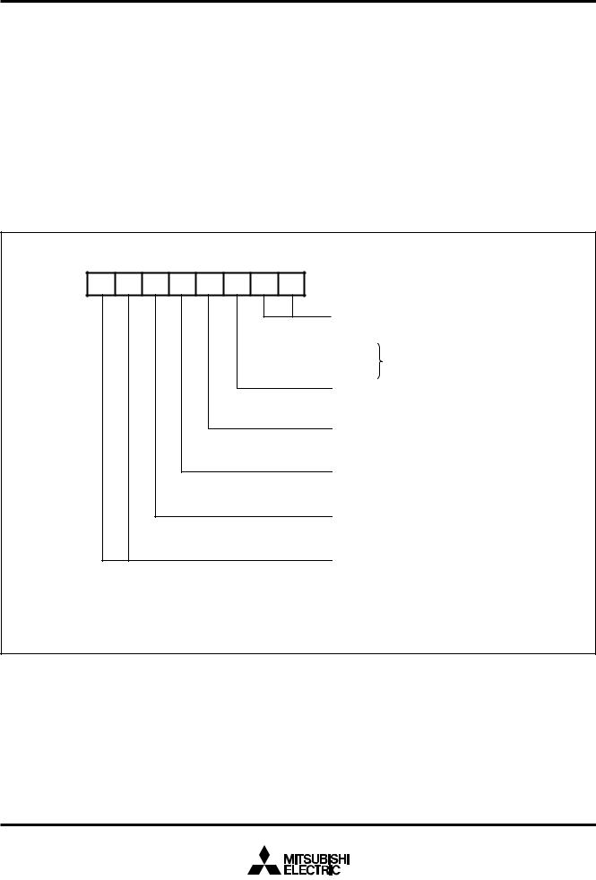
I/O PORTS
The I/O ports have direction registers which determine the input/ output direction of each individual pin. Each bit in a direction register corresponds to one pin, and each pin can be set to be input port or output port.
When “0” is written to the bit corresponding to a pin, that pin becomes an input pin. When “1” is written to that bit, that pin becomes an output pin.
If data is read from a pin which is set to output, the value of the port output latch is read, not the value of the pin itself. Pins set to input are floating. If a pin set to input is written to, only the port output latch is written to and the pin remains floating.
Table 3 I/O port function
|
Pin |
Name |
Input/Output |
I/O Structure |
Non-Port Function |
Related SFRs |
Ref.No. |
|||
P00–P07 |
Port P0 |
|
|
|
|
|
(1) |
|||
|
|
|
|
|
|
CMOS compatible |
|
|
||
P10 |
–P17 |
Port P1 |
|
|
|
|||||
|
|
|
|
|||||||
|
input level |
|
|
|
||||||
|
|
|
|
|
|
|
|
|
||
P20 |
/XCOUT |
|
|
|
|
(2) |
||||
|
|
CMOS 3-state output |
Sub-clock generating |
CPU mode register |
||||||
P21 |
/XCIN |
|
|
|
|
circuit |
(3) |
|||
|
|
|
|
|
||||||
|
|
|
|
|
|
|
|
|
|
|
P22 |
|
|
|
|
|
CMOS compatible |
|
|
|
|
|
|
|
|
|
input level |
|
|
(4) |
||
P23 |
|
|
|
|
|
N-channel open-drain |
|
|
||
|
|
|
|
|
|
|
|
|||
|
|
|
|
|
|
output |
|
|
|
|
|
|
|
|
Port P2 |
|
|
|
|
|
|
P24 |
/RxD |
|
|
|
|
Serial I/O control |
(5) |
|||
|
|
|
|
Serial I/O function I/O |
||||||
P25 |
/TxD |
|
|
|
|
(6) |
||||
|
|
|
|
register |
||||||
|
Input/output, |
|
|
|
||||||
|
|
|
|
|
|
|
|
|
|
|
|
|
|
|
|
individual |
|
|
Serial I/O function I/O |
Serial I/O control |
(7) |
P26 |
/SCLK |
|
bits |
|
|
|||||
|
|
|
register |
|
||||||
|
|
|
|
|
|
|
|
|
|
|
|
|
|
|
|
|
|
|
|
|
|
|
|
|
|
|
|
|
|
Serial I/O function I/O |
Serial I/O control |
(8) |
|
|
|
|
|
|
|
|
register |
||
P27 |
/CNTR0/SRDY |
|
|
CMOS compatible |
Timer X function I/O |
|||||
|
|
|
||||||||
|
|
|
|
|
|
input level |
Timer XY mode register |
|
||
|
|
|
|
|
|
|
|
|||
P30 |
/AN0– |
Port P3 |
|
CMOS 3-state output |
A-D conversion input |
|
(9) |
|||
|
|
|
A-D control register |
|||||||
P34 |
/AN4 |
|
|
|
||||||
|
|
|
|
|
|
|
||||
|
|
|
|
|
|
|
|
|
|
|
P40 |
/CNTR1 |
|
|
|
|
Timer Y function I/O |
Timer XY mode register |
(10) |
||
|
|
|
|
|
|
|
|
|
||
P41 |
/INT0– |
|
|
|
|
External interrupt input |
Interrupt edge selection |
(11) |
||
P43 |
/INT2 |
Port P4 |
|
|
|
register |
||||
|
|
|
|
|
||||||
|
|
|
|
|
|
|
|
|
|
|
|
|
|
|
|
|
|
|
External interrupt input |
Interrupt edge selection |
|
P44 |
/INT3/PWM |
|
|
|
|
register |
(12) |
|||
|
|
|
|
PWM output |
||||||
|
|
|
|
|
|
|
|
PWM control register |
|
|
|
|
|
|
|
|
|
|
|
|
|
9
MITSUBISHI MICROCOMPUTERS
3850 Group
SINGLE-CHIP 8-BIT CMOS MICROCOMPUTER
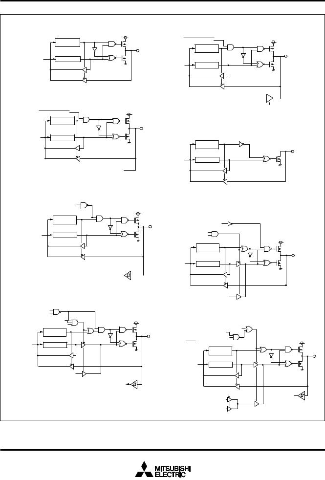
(1) Port P0, P1 |
|
|
Direction |
|
register |
Data bus |
Port latch |
(3) Port P21 |
|
Port XC switch bit |
|
|
Direction |
|
register |
Data bus |
Port latch |
Sub-clock generating circuit input
(5) Port P24
Serial I/O enable bit
Receive enable bit
|
Direction |
|
register |
Data bus |
Port latch |
Serial I/O input 

(7) Port P26
Serial I/O clock selection bit
Serial I/O enable bit
Serial I/O mode selection bit
Serial I/O enable bit
|
Direction |
|
register |
Data bus |
Port latch |
|
Serial clock output |
|
External clock input |
(2) Port P20 |
|
Port XC switch bit |
|
|
Direction |
|
register |
Data bus |
Port latch |
Oscillator
Port P21 

Port XC switch bit
(4) Port P22, P23
|
Direction |
|
register |
Data bus |
Port latch |
(6) Port P25
P-channel output disable bit
Serial I/O enable bit
Transmit enable bit
|
Direction |
|
register |
Data bus |
Port latch |
Serial I/O output
(8) Port P27
Pulse output mode
Serial I/O mode selection bit
Serial I/O enable bit
SRDY output enable bit 
|
Direction |
|
register |
Data bus |
Port latch |
Pulse output mode
Serial ready output
CNTR0 interrupt input
Timer output
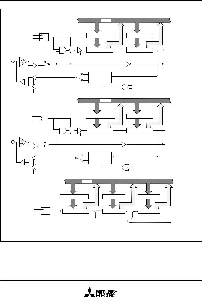
Fig. 8 Port block diagram (1)
10
MITSUBISHI MICROCOMPUTERS
3850 Group
SINGLE-CHIP 8-BIT CMOS MICROCOMPUTER
(9) Port P30–P34 |
|
|
Direction |
|
register |
Data bus |
Port latch |
|
A-D converter input |
Analog input pin selection bit
(11) Port P41–P43 |
|
|
Direction |
|
register |
Data bus |
Port latch |
|
Interrupt input |
(10) Port P40
Data bus
Direction |
register |
Port latch |
Pulse output mode
Timer output
CNTR1 interrupt input
(12) Port P44 |
|
PWM output enable bit |
|
|
Direction |
|
register |
Data bus |
Port latch |
|
PWM output |
Fig. 9 Port block diagram (2)
11

MITSUBISHI MICROCOMPUTERS
3850 Group
SINGLE-CHIP 8-BIT CMOS MICROCOMPUTER
INTERRUPTS
Interrupts occur by 14 sources among 14 sources: six external, seven internal, and one software.
■Notes
When the active edge of an external interrupt (INT0–INT3, CNTR0,
CNTR1) is set, the corresponding interrupt request bit may also be set. Therefore, take the following sequence:
Interrupt Control
Each interrupt is controlled by an interrupt request bit, an interrupt |
1. |
Disable the interrupt |
enable bit, and the interrupt disable flag except for the software in- |
2. |
Change the interrupt edge selection register |
terrupt set by the BRK instruction. An interrupt occurs if the |
|
(the timer XY mode register for CNTR0 and CNTR1) |
corresponding interrupt request and enable bits are “1” and the in- |
3. |
Clear the interrupt request bit to “0” |
terrupt disable flag is “0”. |
4. Accept the interrupt. |
|
Interrupt enable bits can be set or cleared by software. |
|
|
Interrupt request bits can be cleared by software, but cannot be |
|
|
set by software. |
|
|
The BRK instruction cannot be disabled with any flag or bit. The I |
|
|
(interrupt disable) flag disables all interrupts except the BRK in- |
|
|
struction interrupt. |
|
|
When several interrupts occur at the same time, the interrupts are |
|
|
received according to priority. |
|
|
Interrupt Operation
By acceptance of an interrupt, the following operations are automatically performed:
1.The contents of the program counter and the processor status register are automatically pushed onto the stack.
2.The interrupt disable flag is set and the corresponding interrupt request bit is cleared.
3.The interrupt jump destination address is read from the vector table into the program counter.
12

MITSUBISHI MICROCOMPUTERS
3850 Group
SINGLE-CHIP 8-BIT CMOS MICROCOMPUTER
Table 4 Interrupt vector addresses and priority
Interrupt Source |
Priority |
Vector Addresses (Note 1) |
Interrupt Request |
Remarks |
||
High |
Low |
Generating Conditions |
||||
|
|
|
||||
|
|
|
|
|
|
|
Reset (Note 2) |
1 |
FFFD16 |
FFFC16 |
At reset |
Non-maskable |
|
|
|
|
|
|
|
|
INT0 |
2 |
FFFB16 |
FFFA16 |
At detection of either rising or |
External interrupt |
|
falling edge of INT0 input |
(active edge selectable) |
|||||
|
|
|
|
|||
|
|
|
|
|
|
|
Reserved |
3 |
FFF916 |
FFF816 |
Reserved |
|
|
INT1 |
4 |
FFF716 |
FFF616 |
At detection of either rising or |
External interrupt |
|
falling edge of INT1 input |
(active edge selectable) |
|||||
|
|
|
|
|||
|
|
|
|
|
|
|
INT2 |
5 |
FFF516 |
FFF416 |
At detection of either rising or |
External interrupt |
|
falling edge of INT2 input |
(active edge selectable) |
|||||
|
|
|
|
|||
|
|
|
|
|
|
|
INT3 |
6 |
FFF316 |
FFF216 |
At detection of either rising or |
External interrupt |
|
falling edge of INT3 input |
(active edge selectable) |
|||||
|
|
|
|
|||
|
|
|
|
|
|
|
Reserved |
7 |
FFF116 |
FFF016 |
Reserved |
|
|
Timer X |
8 |
FFEF16 |
FFEE16 |
At timer X underflow |
|
|
|
|
|
|
|
|
|
Timer Y |
9 |
FFED16 |
FFEC16 |
At timer Y underflow |
|
|
Timer 1 |
10 |
FFEB16 |
FFEA16 |
At timer 1 underflow |
STP release timer underflow |
|
|
|
|
|
|
|
|
Timer 2 |
11 |
FFE916 |
FFE816 |
At timer 2 underflow |
|
|
Serial I/O |
12 |
FFE716 |
FFE616 |
At completion of serial I/O data |
Valid when serial I/O is selected |
|
reception |
||||||
reception |
||||||
|
|
|
|
|||
|
|
|
|
|
||
|
|
|
|
|
|
|
Serial I/O |
|
|
|
At completion of serial I/O trans- |
|
|
13 |
FFE516 |
FFE416 |
fer shift or when transmission |
Valid when serial I/O is selected |
||
Transmission |
||||||
|
|
|
buffer is empty |
|
||
|
|
|
|
|
||
|
|
|
|
|
|
|
CNTR0 |
14 |
FFE316 |
FFE216 |
At detection of either rising or |
External interrupt |
|
falling edge of CNTR0 input |
(active edge selectable) |
|||||
|
|
|
|
|||
|
|
|
|
|
|
|
CNTR1 |
15 |
FFE116 |
FFE016 |
At detection of either rising or |
External interrupt |
|
falling edge of CNTR1 input |
(active edge selectable) |
|||||
|
|
|
|
|||
|
|
|
|
|
|
|
A-D converter |
16 |
FFDF16 |
FFDE16 |
At completion of A-D conversion |
|
|
BRK instruction |
17 |
FFDD16 |
FFDC16 |
At BRK instruction execution |
Non-maskable software interrupt |
|
|
|
|
|
|
|
|
Notes 1: Vector addresses contain interrupt jump destination addresses.
2: Reset function in the same way as an interrupt with the highest priority.
13
MITSUBISHI MICROCOMPUTERS
3850 Group
SINGLE-CHIP 8-BIT CMOS MICROCOMPUTER
Interrupt request bit 
Interrupt enable bit 
Interrupt disable flag (I)
BRK instruction |
|
|
Interrupt request |
|
|||
Reset |
|
|
|
Fig. 10 Interrupt control
b7
b7
b7
b0 Interrupt edge selection register 


 (INTEDGE : address 003A16)
INT0 active edge selection bit |
|
|
INT1 active edge selection bit |
|
|
INT2 active edge selection bit |
|
|
INT3 active edge selection bit |
|
|
Reserved(Do not write “1” to this bit) |
0 |
: Falling edge active |
Not used (returns “0” when read) |
1 |
: Rising edge active |
b0 Interrupt request register 1
(IREQ1 : address 003C16)
INT0 interrupt request bit
Reserved
INT1 interrupt request bit
INT2 interrupt request bit
INT3 interrupt request bit
Reserved
Timer X interrupt request bit
Timer Y interrupt request bit
0 : No interrupt request issued
1 : Interrupt request issued
b0
Interrupt control register 1 (ICON1 : address 003E16)
INT0 interrupt enable bit
Reserved(Do not write "1" to this bit)
INT1 interrupt enable bit
INT2 interrupt enable bit
INT3 interrupt enable bit
Reserved(Do not write "1" to this bit)
Timer X interrupt enable bit
Timer Y interrupt enable bit
0 : Interrupts disabled
1 : Interrupts enabled
b7
b7
b0 Interrupt request register 2
(IREQ2 : address 003D16)
 Timer 1 interrupt request bit Timer 2 interrupt request bit
Serial I/O reception interrupt request bit Serial I/O transmit interrupt request bit CNTR0 interrupt request bit
CNTR1 interrupt request bit
AD converter interrupt request bit Not used (returns “0” when read)
0 : No interrupt request issued
1 : Interrupt request issued
b0 Interrupt control register 2
(ICON2 : address 003F16)
Timer 1 interrupt enable bit Timer 2 interrupt enable bit
Serial I/O reception interrupt enable bit Serial I/O transmit interrupt enable bit CNTR0 interrupt enable bit
CNTR1 interrupt enable bit
AD converter interrupt enable bit Not used (returns “0” when read) (Do not write “1” to this bit)
0 : Interrupts disabled
1 : Interrupts enabled
Fig. 11 Structure of interrupt-related registers (1)
14
MITSUBISHI MICROCOMPUTERS
3850 Group
SINGLE-CHIP 8-BIT CMOS MICROCOMPUTER
TIMERS
The 3850 group has four timers: timer X, timer Y, timer 1, and timer 2.
The division ratio of each timer or prescaler is given by 1/(n + 1), where n is the value in the corresponding timer or prescaler latch.
All timers are count down. When the timer reaches “0016”, an underflow occurs at the next count pulse and the corresponding timer latch is reloaded into the timer and the count is continued.
When a timer underflows, the interrupt request bit corresponding to that timer is set to “1”.
Timer 1 and Timer 2
The count source of prescaler 12 is the oscillation frequency which is selected by timer 12 count source selection bit. The output of prescaler 12 is counted by timer 1 and timer 2, and a timer underflow sets the interrupt request bit.
Timer X and Timer Y
Timer X and Timer Y can each select in one of four operating modes by setting the timer XY mode register.
b7 |
|
|
b0 |
|
|||||||||||||
|
|
|
|
|
|
|
|
|
|
|
|
|
|
|
|
Timer XY mode register |
|
|
|
|
|
|
|
|
|
|
|
|
|
|
|
|
|
(TM : address 002316) |
|
|
|
|
|
|
|
|
|
|
|
|
|
|
|
|
|
Timer X operating mode bit |
|
|
|
|
|
|
|
|
|
|
|
|
|
|
|
|
|
||
|
|
|
|
|
|
|
|
|
|
|
|
|
|
|
|
b1b0 |
|
|
|
|
|
|
|
|
|
|
|
|
0 |
0: Timer mode |
|||||
|
|
|
|
|
|
|
|
|
|
|
0 |
1: Pulse output mode |
|||||
|
|
|
|
|
|
|
|
|
|
|
1 |
0: Event counter mode |
|||||
|
|
|
|
|
|
|
|
|
|
|
1 |
1: Pulse width measurement mode |
|||||
|
|
|
|
|
|
|
|
|
|
|
|
|
|
|
|
CNTR0 active edge selection bit |
|
|
|
|
|
|
|
|
|
|
|
|
|
|
|
|
|
||
|
|
|
|
|
|
|
|
|
|
|
|
|
|
|
|
|
0: Interrupt at falling edge |
|
|
|
|
|
|
|
|
|
|
|
|
|
|
|
|
|
Count at rising edge in event |
|
|
|
|
|
|
|
|
|
|
|
|
|
|
|
|
|
counter mode |
|
|
|
|
|
|
|
|
|
|
|
|
|
|
|
|
|
1: Interrupt at rising edge |
|
|
|
|
|
|
|
|
|
|
|
|
|
|
|
|
|
Count at falling edge in event |
|
|
|
|
|
|
|
|
|
|
|
|
|
|
|
|
|
counter mode |
|
|
|
|
|
|
|
|
|
|
|
|
|
|
|
|
Timer X count stop bit |
|
|
|
|
|
|
|
|
|
|
|
|
|
|
|
|
|
||
|
|
|
|
|
|
|
|
|
|
|
|
|
|
|
|
|
0: Count start |
|
|
|
|
|
|
|
|
|
|
|
|
|
|
|
|
|
1: Count stop |
|
|
|
|
|
|
|
|
|
|
|
|
|
|
|
|
Timer Y operating mode bit |
|
|
|
|
|
|
|
|
|
|
|
|
|
|
|
|
|||
|
|
|
|
|
|
|
|
|
|
|
|
|
|
|
|
b5b4 |
|
|
|
|
|
|
|
|
|
|
|
|
0 |
0: Timer mode |
|||||
|
|
|
|
|
|
|
|
|
|
|
0 |
1: Pulse output mode |
|||||
|
|
|
|
|
|
|
|
|
|
|
1 |
0: Event counter mode |
|||||
|
|
|
|
|
|
|
|
|
|
|
1 |
1: Pulse width measurement mode |
|||||
|
|
|
|
|
|
|
|
|
|
|
|
|
|
|
|
CNTR1 active edge selection bit |
|
|
|
|
|
|
|
|
|
|
|
|
|
|
|
|
|
||
|
|
|
|
|
|
|
|
|
|
|
|
|
|
|
|
|
0: Interrupt at falling edge |
|
|
|
|
|
|
|
|
|
|
|
|
|
|
|
|
|
Count at rising edge in event |
|
|
|
|
|
|
|
|
|
|
|
|
|
|
|
|
|
counter mode |
|
|
|
|
|
|
|
|
|
|
|
|
|
|
|
|
|
1: Interrupt at rising edge |
|
|
|
|
|
|
|
|
|
|
|
|
|
|
|
|
|
Count at falling edge in event |
|
|
|
|
|
|
|
|
|
|
|
|
|
|
|
|
|
counter mode |
|
|
|
|
|
|
|
|
|
|
|
|
|
|
|
|
Timer Y count stop bit |
|
|
|
|
|
|
|
|
|
|
|
|
|
|
|
|
|
||
|
|
|
|
|
|
|
|
|
|
|
|
|
|
|
|
|
0: Count start |
|
|
|
|
|
|
|
|
|
|
|
|
|
|
|
|
|
1: Count stop |
Fig. 12 Structure of timer XY mode register
b7 |
b0 |
Timer count source selection register (TCSS : address 002816)
Timer X count source selection bit
0 : f(XIN)/16 (f(XCIN)/16 at low-speed mode) 1 : f(XIN)/2 (f(XCIN)/2 at low-speed mode)
Timer Y count source selection bit
0 : f(XIN)/16 (f(XCIN)/16 at low-speed mode) 1 : f(XIN)/2 (f(XCIN)/2 at low-speed mode)
Timer 12 count source selection bit
0 : f(XIN)/16 (f(XCIN)/16 at low-speed mode) 1 : f(XCIN)
Not used (returns “0” when read)
Fig. 13 Structure of timer count source selection register
(1) Timer Mode
The timer counts the count source selected by Timer count source selection bit.
(2) Pulse Output Mode
The timer counts the count source selected by Timer count source selection bit. Whenever the contents of the timer reach “0016”, the signal output from the CNTR0 (or CNTR1) pin is inverted. If the CNTR0 (or CNTR1) active edge selection bit is “0”, output begins at “ H”.
If it is “1”, output starts at “L”. When using a timer in this mode, set the corresponding port P27 ( or port P40) direction register to output mode.
(3) Event Counter Mode
Operation in event counter mode is the same as in timer mode, except that the timer counts signals input through the CNTR0 or CNTR1 pin.
When the CNTR0 (or CNTR1) active edge selection bit is “0”, the rising edge of the CNTR0 (or CNTR1) pin is counted.
When the CNTR0 (or CNTR1) active edge selection bit is “1”, the falling edge of the CNTR0 (or CNTR1) pin is counted.
(4) Pulse Width Measurement Mode
If the CNTR0 (or CNTR1) active edge selection bit is “0”, the timer counts the selected signals by the count source selection bit while the CNTR0 (or CNTR1) pin is at “H”. If the CNTR0 (or CNTR1) active edge selection bit is “1”, the timer counts it while the CNTR0
(or CNTR1) pin is at “L”.
The count can be stopped by setting “1” to the timer X (or timer Y) count stop bit in any mode. The corresponding interrupt request bit is set each time a timer underflows.
■Note
When switching the count source by the timer 12, X and Y count source bit, the value of timer count is altered in unconsiderable amount owing to generating of a thin pulses in the count input signals.
Therefore, select the timer count source before set the value to the prescaler and the timer.
15
MITSUBISHI MICROCOMPUTERS
3850 Group
SINGLE-CHIP 8-BIT CMOS MICROCOMPUTER
|
|
|
|
|
|
|
Data bus |
|
|
f(XIN)/16 |
|
|
|
|
|
Prescaler X latch (8) |
Timer X latch (8) |
|
|
f(XIN)/2 |
|
|
Pulse width |
|
|
|
|
|
|
Timer X count source selection bit |
Timer mode |
|
|
|
|
||||
measurement |
|
|
|
|
|||||
|
|
|
mode |
Pulse output mode |
|
To timer X interrupt |
|||
|
|
|
|
|
|
|
|||
|
|
|
|
|
|
|
Prescaler X (8) |
Timer X (8) |
|
|
|
|
|
|
|
|
request bit |
||
|
CNTR0 active |
|
Event |
Timer X count stop bit |
|
|
|||
|
edge selection |
|
|
||||||
P27/CNTR0 |
counter |
|
|
||||||
“0” |
bit |
|
|
|
|
|
|||
|
mode |
|
|
|
|
To CNTR0 interrupt |
|||
|
|
|
|
|
|
|
|
||
|
|
|
|
|
|
|
|
|
|
|
|
|
|
|
|
|
|
|
request bit |
|
“1” |
|
|
CNTR0 active |
|
|
|
|
|
|
|
|
|
|
|
|
|
||
|
|
|
|
edge selection “1” |
Q |
|
|
|
|
|
|
|
|
bit |
|
Toggle flip-flop T |
|
|
|
|
|
|
|
|
|
|
|
||
|
|
|
|
|
|
|
|
|
|
|
|
|
|
|
“0” |
Q |
R |
|
|
|
|
|
|
|
|
Timer X latch write pulse |
|
||
|
Port P27 |
|
|
|
|
|
|
|
|
Port P27 |
|
|
|
|
|
|
Pulse output mode |
|
|
latch |
|
|
|
|
|
|
|
||
direction register |
|
|
|
|
|
|
|
|
|
Pulse output mode |
|
|
|
|
|
|
|
|
|
|
|
|
|
|
|
|
Data bus |
|
|
f(XIN)/16 |
|
|
|
|
|
Prescaler Y latch (8) |
Timer Y latch (8) |
|
|
f(XIN)/2 |
|
|
|
Pulse width |
|
|
|
|
|
|
|
|
|
Timer mode |
|
|
|
|
|
Timer Y count source selection bit |
|
measure- |
|
|
|
|
|||
|
ment mode |
Pulse output mode |
|
|
|||||
|
|
|
|
|
|
||||
|
|
|
|
|
|
|
Prescaler Y (8) |
Timer Y (8) |
To timer Y interrupt |
|
CNTR1 active |
|
|
|
|
|
|
request bit |
|
|
|
Event |
|
|
|
|
|
||
P40/CNTR1 |
edge selection |
|
Timer Y count stop bit |
|
|
||||
“0” |
bit |
|
counter |
|
|
|
|
|
|
|
|
|
|
|
|
|
|||
|
|
|
|
mode |
|
|
|
|
To CNTR1 interrupt |
|
|
|
|
|
|
|
|
|
|
|
“1” |
|
|
|
|
|
|
|
request bit |
|
|
|
CNTR1 active |
|
|
|
|
||
|
|
|
|
|
|
|
|
||
|
|
|
|
edge selection “1” |
Q |
|
|
|
|
|
|
|
|
bit |
|
Toggle flip-flop T |
|
|
|
|
|
|
|
|
|
|
|
|
|
|
|
|
|
|
“0” |
Q |
R |
|
|
|
|
|
|
|
|
|
|
||
|
Port P40 |
|
|
|
|
|
Timer Y latch write pulse |
|
|
|
|
|
|
|
|
|
|
||
Port P40 |
latch |
|
|
|
|
|
|
Pulse output mode |
|
|
|
|
|
|
|
|
|
||
direction register
Pulse output mode
|
Data bus |
|
|
|
Prescaler 12 latch (8) |
Timer 1 latch (8) |
|
f(XIN)/16 |
Prescaler 12 (8) |
Timer 1 (8) |
|
f(XCIN) |
|||
|
|
||
Timer 12 count source selection bit |
|
|
Timer 2 latch (8)
Timer 2 (8)
 To timer 2 interrupt request bit
 To timer 1 interrupt request bit
Fig. 14 Block diagram of timer X, timer Y, timer 1, and timer 2
16
Loading...