


 Loading...
MITSUBISHI MICROCOMPUTERS
3850 Group (Spec. H)
SINGLE-CHIP 8-BIT CMOS MICROCOMPUTER
DESCRIPTION
The 3850 group (spec. H) is the 8-bit microcomputer based on the 740 family core technology.
The 3850 group (spec. H) is designed for the household products and office automation equipment and includes serial I/O functions, 8-bit timer, and A-D converter.
FEATURES |
|
|
●Basic machine-language instructions |
...................................... 71 |
|
●Minimum instruction execution time .................................. |
0.5 μs |
|
|
(at 8 MHz oscillation frequency) |
|
●Memory size |
|
|
ROM ................................................................... |
|
8K to 32K bytes |
RAM ................................................................. |
|
512 to 1024 bytes |
●Programmable input/output ports ............................................ |
34 |
|
●Interrupts ................................................. |
|
14 sources, 14 vectors |
●Timers ............................................................................. |
|
8 - bit 4 |
●Serial I/O1 .................... |
8-bit 1(UART or Clock-synchronized) |
|
●Serial I/O2 ................................... |
8-bit 1(Clock-synchronized) |
|
●PWM ............................................................................... |
|
8 - bit 1 |
●A-D converter ............................................... |
|
10 - bit 5 channels |
●Watchdog timer ............................................................ |
|
16 - bit 1 |
●Clock generating circuit ..................................... |
|
Built - in 2 circuits |
(connect to external ceramic resonator or quartz-crystal oscillator) |
||
●Power source voltage |
|
In high-speed mode .................................................. |
4.0 to 5.5 V |
(at 8 MHz oscillation frequency) |
|
In middle-speed mode ............................................... |
2.7 to 5.5 V |
(at 8 MHz oscillation frequency) |
|
In low-speed mode .................................................... |
2.7 to 5.5 V |
(at 32 kHz oscillation frequency) |
|
●Power dissipation |
|
In high-speed mode .......................................................... |
34 mW |
(at 8 MHz oscillation frequency, at 5 V power source voltage) |
|
In low-speed mode ............................................................ |
60 μW |
(at 32 kHz oscillation frequency, at 3 V power source voltage) |
|
●Operating temperature range .................................... |
–20 to 85°C |
APPLICATION
Office automation equipment, FA equipment, Household products, Consumer electronics, etc.
PIN CONFIGURATION (TOP VIEW)
|
|
VCC |
1 |
|||||||||
|
|
VREF |
|
|
|
|
|
|
|
|
||
|
|
|
|
|
|
|
|
2 |
||||
|
||||||||||||
|
|
AVSS |
|
|
|
|
|
|
|
|
|
|
P44/INT3/PWM |
|
|
|
|
|
|
|
3 |
||||
|
|
|
|
|
|
|
|
|||||
|
|
|
|
|
|
4 |
||||||
P43/INT2/SCMP2 |
|
|
|
|
|
|
|
|
||||
|
|
|
|
|
|
5 |
||||||
P42/INT1 |
|
|
|
|
|
|
|
|
||||
|
|
|
|
|
|
6 |
||||||
P41/INT0 |
|
|
|
|
|
|
|
|
||||
|
|
|
|
|
|
7 |
||||||
P40/CNTR1 |
|
|
|
|
|
|
|
|
||||
|
|
|
|
|
|
8 |
||||||
|
|
|
|
|
|
|
|
|||||
P27/CNTR0/SRDY1 |
|
|
|
|
|
|||||||
|
|
|
|
|
9 |
|||||||
|
|
|
|
|
|
|||||||
P26/SCLK |
|
|
|
|
||||||||
|
|
|
|
|
10 |
|||||||
|
|
|
|
|
|
|||||||
P25/TxD |
|
|
|
|
||||||||
|
|
|
|
|
11 |
|||||||
|
|
|
|
|
|
|||||||
P24/RxD |
|
|
|
|||||||||
|
|
|
|
12 |
||||||||
|
|
|
|
|
|
|||||||
|
|
P23 |
|
|
|
|||||||
|
|
|
|
13 |
||||||||
|
|
|
|
|
|
|||||||
|
|
P22 |
|
|
|
|
|
|
|
|||
|
|
|
|
|
14 |
|||||||
|
CNVSS |
|
|
|
|
|
||||||
|
|
|
15 |
|||||||||
P21/XCIN |
|
|
|
|
|
|
||||||
|
|
|
|
|
|
16 |
||||||
|
|
|||||||||||
P20/XCOUT |
|
|
|
|
|
|
||||||
|
|
|
|
|
|
17 |
||||||
|
|
|||||||||||
|
RESET |
|
|
|
|
|
|
|||||
|
|
|
18 |
|||||||||
|
|
XIN |
|
|
|
|
||||||
|
19 |
|||||||||||
|
|
XOUT |
|
|
|
|
|
|
|
|
||
|
|
|
|
|
|
|
||||||
|
|
|
|
20 |
||||||||
|
||||||||||||
|
|
VSS |
|
|
|
|
|
|||||
|
|
|
|
|
21 |
|||||||
|
||||||||||||
XXXFP-38503M4HM XXXSP-M38503M4H
42 |
|
|
|
|
P30/AN0 |
||
|
|
|
|||||
|
|
|
|
|
P31/AN1 |
||
41 |
|
|
|
|
|||
|
|
|
|||||
|
|
|
|
|
P32/AN2 |
||
40 |
|
|
|
|
|||
|
|
|
|||||
|
|
|
|
|
P33/AN3 |
||
39 |
|
|
|
|
|||
|
|
|
|
|
P34/AN4 |
||
38 |
|
|
|
|
|||
|
|
|
|
|
P00/SIN2 |
||
37 |
|
|
|
|
|||
|
|
|
|
|
P01/SOUT2 |
||
36 |
|
|
|
|
|||
|
|
|
|
|
P02/SCLK2 |
||
35 |
|
|
|
|
|||
|
|
|
|
|
|
|
|
|
|
|
|
|
P03/SRDY2 |
|
|
34 |
|
|
|
|
|||
|
|
|
|||||
|
|
|
|||||
|
|
|
|
|
P04 |
||
33 |
|
|
|
|
|||
|
|
|
|||||
|
|
|
|||||
|
|
|
|
|
P05 |
||
32 |
|
|
|
|
|||
|
|
|
|||||
|
|
|
|||||
|
|
|
|
|
P06 |
||
31 |
|
|
|
|
|||
|
|
|
|
||||
|
|
|
|
|
P07 |
||
30 |
|
|
|
|
|||
|
|
|
|
||||
|
|
|
|
|
P10/(LED0) |
||
29 |
|
|
|
|
|||
|
|
|
|
|
P11/(LED1) |
||
28 |
|
|
|
|
|||
|
|
|
|
|
P12/(LED2) |
||
27 |
|
|
|
|
|||
|
|
|
|
||||
|
|
|
|
|
P13/(LED3) |
||
26 |
|
|
|
|
|||
|
|
|
|
||||
|
|
|
|
|
P14/(LED4) |
||
25 |
|
|
|
|
|||
|
|
|
|
||||
|
|
|
|
|
P15/(LED5) |
||
24 |
|
|
|
|
|||
|
|
|
|||||
|
|
|
|
|
P16/(LED6) |
||
|
|
|
|
|
|||
23 |
|
|
|
|
|||
|
|
|
|||||
|
|
|
|
|
P17/(LED7) |
||
22 |
|
|
|
|
|||
|
|
|
|||||
Package type : |
FP ........................... |
42P2R-A/E (42-pin plastic-molded SSOP) |
Package type : |
SP ........................... |
42P4B (42-pin plastic-molded SDIP) |
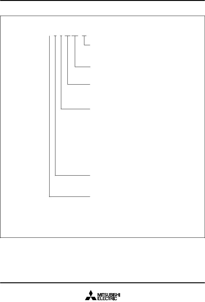
Fig. 1 M38503M4H-XXXFP/SP pin configuration

2 |
diagramblockFunctional 2 .Fig |
|
|
|
|
|
|
|
|
|
|
|
|
|
|
|
|
|
BLOCKFUNCTIONAL |
|
|
|
FUNCTIONAL BLOCK DIAGRAM |
|
|
|
|
|
|
|
|
|
|
|
|
|
|||||||
|
Main-clock |
Main-clock |
|
|
|
|
|
|
|
Reset input |
|
|
|
|
|
|
|
|
|
|
|
|
input |
output |
|
|
|
|
|
|
|
|
|
CNVSS |
|
|
|
|
|
|
|
|
|
|
XIN |
XOUT |
|
|
|
|
|
|
VSS |
VCC |
RESET |
|
|
|
|
|
|
|
|
||
|
19 |
20 |
|
|
|
|
|
|
21 |
1 |
18 |
|
15 |
|
|
|
|
|
|
|
|
|
|
Sub-clock Sub-clock |
|
|
|
|
|
|
|
|
|
|
|
|
|
|
|
|
|
||
|
|
|
input |
output |
|
|
|
|
|
|
|
|
|
|
|
|
|
|
|
|
|
|
|
|
XCIN |
XCOUT |
|
|
|
|
|
|
|
|
|
|
|
|
|
|
|
|
|
|
Clock generating circuit |
|
|
|
|
|
|
|
|
|
|
|
Timer |
1( 8 ) |
|
|
|
|
|||
|
|
|
|
|
|
|
|
|
|
|
|
|
|
|
|
|
|
|
|
||
|
|
|
|
|
|
|
|
|
|
|
|
|
|
Prescaler |
12(8) |
Timer |
2( 8 ) |
|
|
|
|
|
|
|
|
|
|
|
|
|
|
|
|
|
|
Prescaler |
X(8) |
Timer |
X( 8 ) |
|
|
|
|
|
|
|
|
|
|
|
|
|
|
|
|
|
CNTR0 |
Prescaler |
Y(8) |
Timer |
Y( 8 ) |
|
|
|
|
|
Watchdog |
|
|
|
|
|
|
|
|
|
|
|
|
|
|
|
|||||
|
|
Reset |
|
|
|
|
|
|
|
|
|
|
|
|
|
|
|
|
|
||
|
|
timer |
|
|
|
|
|
|
|
|
|
|
|
|
|
|
|
|
|
|
|
|
|
|
|
|
|
|
|
|
|
|
|
|
|
|
|
|
|
|
|
|
|
|
|
|
|
|
|
|
|
|
|
|
|
|
|
CNTR1 |
|
|
|
|
|
|
|
|
|
|
A-D |
PWM |
|
|
|
|
|
SI/O1(8) |
|
|
|
|
|
|
|
SI/O2(8) |
SINGLE |
|
|
|
|
converter |
(8) |
|
|
|
|
|
|
|
|
|
|
|
|
|
|
|
|
|
|
|
|
|
(10) |
|
|
|
|
|
|
|
|
|
|
XCOUT |
|
|
|
|
|
|
|
|
|
|
|
|
|
|
|
|
|
|
|
|
|
|
|
|
|
|
|
|
|
|
|
|
|
|
|
|
|
|
|
|
|
|
|
XCIN |
|
|
|
|
MICROCOMPUTERCMOSBIT-8CHIP- |
H).(SpecGroup3850 |
MICROCOMPUTERSMITSUBISHI |
|
|
|
|
|
|
|
|
INT0– |
|
|
|
|
|
|
|
|
|
|
|||
|
|
|
|
|
|
|
|
INT3 |
|
|
|
|
|
|
|
|
|
|
|
|
|
|
|
|
|
|
P4(5) |
|
P3(5) |
|
|
|
P2(8) |
|
P1(8) |
P0(8) |
|
|
|
|
|||
|
|
2 |
3 |
4 |
5 |
6 |
7 |
8 |
38 39 40 41 42 |
|
|
9 |
10 11 12 13 1416 17 |
22 23 24 25 26 27 28 29 |
30 31 32 33 34 35 36 37 |
|
|
|
|
||
|
|
|
|
I/O port P4 |
I/O port P3 |
|
|
|
I/O port P2 |
|
I/O port P1 |
I/O port P0 |
|
|
|
|
|||||
|
|
VREF |
|
|
|
|
|
|
|
|
|
|
|
|
|
|
|
|
|
|
|
|
|
AVSS |
|
|
|
|
|
|
|
|
|
|
|
|
|
|
|
|
|
|
|

MITSUBISHI MICROCOMPUTERS
3850 Group (Spec. H)
SINGLE-CHIP 8-BIT CMOS MICROCOMPUTER
PIN DESCRIPTION
Table 1 Pin description
|
|
Pin |
Name |
Functions |
|
|||
Function except a port function |
||||||||
|
|
|
|
|
|
|
||
|
|
|
|
|
|
|
|
|
|
VCC, VSS |
Power source |
•Apply voltage of 2.7 V – 5.5 V to Vcc, and 0 V to Vss. |
|
||||
|
|
|
|
|
|
|
|
|
|
CNVSS |
CNVSS input |
•This pin controls the operation mode of the chip. |
|
||||
|
•Normally connected to VSS. |
|
||||||
|
|
|
|
|
|
|
||
|
|
|
|
|
|
|
|
|
|
|
|
|
Reset input |
•Reset input pin for active “L.” |
|
||
|
RESET |
|
|
|
||||
|
XIN |
Clock input |
•Input and output pins for the clock generating circuit. |
|
||||
|
•Connect a ceramic resonator or quartz-crystal oscillator between the XIN and XOUT pins to set |
|||||||
|
|
|
|
|
|
|||
|
|
|
|
|
|
the oscillation frequency. |
|
|
|
|
|
|
|
|
|
||
|
XOUT |
Clock output |
•When an external clock is used, connect the clock source to the XIN pin and leave the XOUT |
|||||
|
|
|
|
|
|
pin open. |
|
|
|
P00/SIN2 |
|
•8-bit CMOS I/O port. |
• Serial I/O2 function pin |
||||
|
P01/SOUT2 |
|
•I/O direction register allows each pin to be individually |
|
||||
|
P02/SCLK2 |
I/O port P0 |
programmed as either input or output. |
|
||||
|
|
•CMOS compatible input level. |
|
|||||
|
|
|
|
|
|
|
||
|
P03/SRDY2 |
|
|
|||||
|
|
•CMOS 3-state output structure. |
|
|||||
|
P04–P07 |
|
|
|||||
|
|
•P10 to P17 (8 bits) are enabled to output large current for LED drive. |
||||||
|
|
|
|
|
|
|||
|
P10–P17 |
I/O port P1 |
||||||
|
|
|
||||||
|
|
|
|
|
|
|
||
|
P20/XCOUT |
|
•8-bit CMOS I/O port. |
• Sub-clock generating circuit I/O |
||||
|
P21/XCIN |
|
•I/O direction register allows each pin to be individually |
pins (connect a resonator) |
||||
|
|
|
||||||
|
P22 |
I/O port P2 |
programmed as either input or output. |
|
||||
|
P23 |
•CMOS compatible input level. |
|
|||||
|
|
|
||||||
|
P24/RxD |
|
•P20, P21, P24 to P27: CMOS3-state output structure. |
• Serial I/O1 function pin |
||||
|
P25/TxD |
|
•P22, P23: N-channel open-drain structure. |
|
||||
|
P26/SCLK |
|
|
|
||||
|
P27/CNTR0/ |
|
|
• Serial I/O1 function pin/ |
||||
|
SRDY1 |
|
|
Timer X function pin |
||||
|
|
|
|
|
|
|
|
|
|
P30/AN0– |
|
•8-bit CMOS I/O port with the same function as port P0. |
• A-D converter input pin |
||||
|
I/O port P3 |
•CMOS compatible input level. |
|
|||||
|
P34/AN4 |
|
||||||
|
|
•CMOS 3-state output structure. |
|
|||||
|
|
|
|
|
|
|
||
|
|
|
|
|
|
|
||
|
P40/CNTR1 |
|
•8-bit CMOS I/O port with the same function as port P0. |
• Timer Y function pin |
||||
|
P41/INT0 |
I/O port P4 |
•CMOS compatible input level. |
• Interrupt input pins |
||||
|
P42/INT1 |
|
•CMOS 3-state output structure. |
|
||||
|
P43/INT2/SCMP2 |
|
|
• Interrupt input pin |
||||
|
|
|
• SCMP2 output pin |
|||||
|
|
|
|
|
|
|
||
|
P44/INT3/PWM |
|
|
• Interrupt input pin |
||||
|
|
|
• PWM output pin |
|||||
|
|
|
|
|
|
|
||
|
|
|
|
|
|
|
|
|
3
MITSUBISHI MICROCOMPUTERS
3850 Group (Spec. H)
SINGLE-CHIP 8-BIT CMOS MICROCOMPUTER
PART NUMBERING
Product name |
M3850 3 M 4 H– XXX SP |
||
|
|
|
|
Package type
SP : 42P4B
FP : 42P2R-A/E
SS : 42S1B-A
ROM number
Omitted in One Time PROM version shipped in blank,
EPROM version, and flash memory version.
– : standard
Omitted in One Time PROM version shipped in blank, EPROM version, and flash memory version.
H–: Partial specification changed version
ROM/PROM/Flash memory size
1 |
: 4096 bytes |
9 : 36864 bytes |
2 |
: 8192 bytes |
A : 40960 bytes |
3 |
: 12288 bytes |
B : 45056 bytes |
4 |
: 16384 bytes |
C : 49152 bytes |
5 |
: 20480 bytes |
D : 53248 bytes |
6 |
: 24576 bytes |
E : 57344 bytes |
7 |
: 28672 bytes |
F : 61440 bytes |
8 |
: 32768 bytes |
|
The first 128 bytes and the last 2 bytes of ROM are reserved areas ; they cannot be used as a user’s ROM area.
However, they can be programmed or erased in the flash memory version, so that the users can use them.
Memory type
M : Mask ROM version
E : EPROM or One Time PROM version
F : Flash memory version
RAM size |
|
|
0 : 192 bytes |
5 |
: 768 bytes |
1 : 256 bytes |
6 |
: 896 bytes |
2 : 384 bytes |
7 |
: 1024 bytes |
3 : 512 bytes |
8 |
: 1536 bytes |
4 : 640 bytes |
9 |
: 2048 bytes |
Fig. 3 Part numbering
4
MITSUBISHI MICROCOMPUTERS
3850 Group (Spec. H)
SINGLE-CHIP 8-BIT CMOS MICROCOMPUTER
GROUP EXPANSION
Mitsubishi plans to expand the 3850 group (spec. H) as follows.
Memory Type
Support for mask ROM, One Time PROM, and flash memory versions.
Packages
42P4B ......................................... |
42-pin shrink plastic-molded DIP |
42P2R-A/E ........................................... |
42-pin plastic-molded SOP |
42S1B-A .................. |
42-pin shrink ceramic DIP (EPROM version) |
Memory Size
Flash memory size ......................................................... |
32 |
K bytes |
One Time PROM size ..................................................... |
24 |
K bytes |
Mask ROM size ................................................... |
8 K to 32 |
K bytes |
RAM size ............................................................... |
512 to 1 |
K bytes |
Memory Expansion Plan
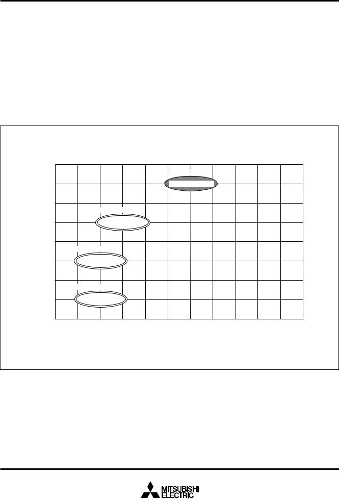
ROM size (bytes)
As of Feb. 2000
ROM |
|
exteranal |
Under development |
|
|
32K |
M38507M8/F8 |
28K |
Mass production |
|
|
24K |
M38504M6/E6 |
20K
Mass production
16K M38503M4H
12K
Mass production
8K M38503M2H
384 |
512 |
640 |
768 |
896 |
1024 |
1152 |
1280 |
1408 |
1536 |
2048 |
RAM size (bytes)
Products under development or planning: the development schedule and specification may be revised without notice. The development of planning products may be stopped.
Fig. 4 Memory expansion plan
5

MITSUBISHI MICROCOMPUTERS
3850 Group (Spec. H)
SINGLE-CHIP 8-BIT CMOS MICROCOMPUTER
Currently planning products are listed below.
Table 2 Support products |
|
|
|
As of Feb. 2000 |
||
|
|
|
|
|
|
|
Product name |
ROM size (bytes) |
|
RAM size (bytes) |
Package |
Remarks |
|
ROM size for User in ( |
) |
|||||
|
|
|
|
|||
M38503M2H-XXXSP |
8192 |
|
512 |
42P4B |
Mask ROM version |
|
M38503M2H-XXXFP |
(8062) |
|
42P2R-A/E |
Mask ROM version |
||
|
|
|||||
M38503M4H-XXXSP |
16384 |
|
512 |
424P4B |
Mask ROM version |
|
M38503M4H-XXXFP |
(16254) |
|
42P2R-A/E |
Mask ROM version |
||
|
|
|||||
M38504M6-XXXSP |
|
|
|
|
Mask ROM version |
|
M38504E6-XXXSP |
|
|
|
424P4B |
One Time PROM version |
|
M388504E6SP |
24576 |
|
|
|
One Time PROM version (blank) |
|
M388504E6SS |
|
640 |
42S1B-A |
EPROM version |
||
(24446) |
|
|||||
M38504M6-XXXFP |
|
|
|
Mask ROM version |
||
|
|
|
|
|||
M38504E6-XXXFP |
|
|
|
42P2R-A/E |
One Time PROM version |
|
M38504E6FP |
|
|
|
|
One Time PROM version (blank) |
|
Table 3 3850 group (standard) and 3850 group (spec. H)
corresponding products
3850 group (standard) |
3850 group (spec. H) |
M38503M2-XXXFP/SP |
M38503M2H-XXXFP/SP |
M38503M4-XXXFP/SP |
M38503M4H-XXXFP/SP |
M38503E4-XXXFP/SP |
M38504M6-XXXFP/SP |
M38503E4FP/SP |
M38504E6-XXXFP/SP |
M38503E4SS |
M38504E6FP/SP |
|
M38504E6SS |
|
M38507M8-XXXFP/SP |
|
M38507F8FP/SP |
|
|
Table 4 Differences between 3850 group (standard) and 3850 group (spec. H)
|
3850 group (standard) |
3850 group (spec. H) |
Serial I/O |
1: Serial I/O (UART or Clock-synchronized) |
2: Serial I/O1 (UART or Clock-synchronized) |
|
|
Serial I/O2 (Clock-synchronized) |
A-D converter |
Unserviceable in low-speed mode |
Serviceable in low-speed mode |
Large current port |
5: P13–P17 |
8: P10–P17 |
Notes on differences between 3850 group (standard) and 3850 group (spec. H)
(1)The absolute maximum ratings of 3850 group (spec. H) is smaller than that of 3850 group (standard).
•Power source voltage Vcc = –0.3 to 6.5 V
•CNVss input voltage VI = –0.3 to Vcc +0.3 V
(2)The oscillation circuit constants of XIN-XOUT, XCIN-XCOUT may be some differences between 3850 group (standard) and 3850 group (spec. H).
(3)Do not write any data to the reserved area and the reserved bit. (Do not change the contents after rest.)
(4)Fix bit 3 of the CPU mode register to “1”.
(5)Be sure to perform the termination of unused pins.
6

MITSUBISHI MICROCOMPUTERS
3850 Group (Spec. H)
SINGLE-CHIP 8-BIT CMOS MICROCOMPUTER
FUNCTIONAL DESCRIPTION CENTRAL PROCESSING UNIT (CPU)
The 3850 group (spec. H) uses the standard 740 Family instruction set. Refer to the table of 740 Family addressing modes and machine instructions or the 740 Family Software Manual for details on the instruction set.
Machine-resident 740 Family instructions are as follows:
The FST and SLW instructions cannot be used.
The STP, WIT, MUL, and DIV instructions can be used.
[Accumulator (A)]
The accumulator is an 8-bit register. Data operations such as data transfer, etc., are executed mainly through the accumulator.
[Index Register X (X)]
The index register X is an 8-bit register. In the index addressing modes, the value of the OPERAND is added to the contents of register X and specifies the real address.
[Index Register Y (Y)]
The index register Y is an 8-bit register. In partial instruction, the value of the OPERAND is added to the contents of register Y and specifies the real address.
[Stack Pointer (S)]
The stack pointer is an 8-bit register used during subroutine calls and interrupts. This register indicates start address of stored area (stack) for storing registers during subroutine calls and interrupts. The low-order 8 bits of the stack address are determined by the contents of the stack pointer. The high-order 8 bits of the stack address are determined by the stack page selection bit. If the stack page selection bit is “0” , the high-order 8 bits becomes “0016”. If the stack page selection bit is “1”, the high-order 8 bits becomes “0116”.
The operations of pushing register contents onto the stack and popping them from the stack are shown in Figure 6.
Store registers other than those described in Figure 6 with program when the user needs them during interrupts or subroutine calls.
[Program Counter (PC)]
The program counter is a 16-bit counter consisting of two 8-bit registers PCH and PCL. It is used to indicate the address of the next instruction to be executed.
|
|
b7 |
|
|
b0 |
||||||||||||||
|
|
|
|
|
|
|
|
|
|
|
|
|
|
|
|
|
|
|
|
|
|
|
|
|
|
|
|
|
A |
|
|
|
|
|
Accumulator |
||||
|
|
|
|
|
|
|
|
|
|
|
|
|
|
|
|
|
|
|
|
|
|
b7 |
|
|
b0 |
||||||||||||||
|
|
|
|
|
|
|
|
|
X |
|
|
|
|
|
Index register X |
||||
|
|
|
|
|
|
|
|
|
|
|
|
|
|
|
|
|
|
|
|
|
|
b7 |
|
|
b0 |
||||||||||||||
|
|
|
|
|
|
|
|
|
Y |
|
|
|
|
|
Index register Y |
||||
|
|
|
|
|
|
|
|
|
|
|
|
|
|
|
|
|
|
|
|
|
|
b7 |
|
|
b0 |
||||||||||||||
|
|
|
|
|
|
|
|
|
S |
|
|
|
|
|
Stack pointer |
||||
|
|
|
|
|
|
|
|
|
|
|
|
|
|
|
|
|
|
|
|
|
b15 |
b7 |
|
|
b0 |
||||||||||||||
|
PCH |
|
|
|
|
|
|
PCL |
|
|
|
|
|
Program counter |
|||||
|
|
|
|
|
|
|
|
|
|
|
|
|
|
|
|
|
|
|
|
|
|
b7 |
|
|
b0 |
||||||||||||||
|
|
N |
V |
T |
B |
D |
I |
Z |
C |
|
Processor status register (PS) |
||||||||
|
|
|
|
|
|
|
|
|
|
|
|
|
|
|
|
|
|
|
Carry flag |
|
|
|
|
|
|
|
|
|
|
|
|
|
|
|
|
|
|
|
|
|
|
|
|
|
|
|
|
|
|
|
|
|
|
|
|
|
|
|
|
|
|
|
|
|
|
|
|
|
|
|
|
|
|
|
|
|
|
|
Zero flag |
|
|
|
|
|
|
|
|
|
|
|
|
|
|
|
|
|
|
|
|
|
|
|
|
|
|
|
|
|
|
|
|
|
|
|
|
|
|
|
Interrupt disable flag |
|
|
|
|
|
|
|
|
|
|
|
|
|
|
|
|
|
|
|
|
|
|
|
|
|
|
|
|
|
|
|
|
|
|
|
|
|
|
|
Decimal mode flag |
|
|
|
|
|
|
|
|
|
|
|
|
|
|
|
|
|
|
|
|
|
|
|
|
|
|
|
|
|
|
|
|
|
|
|
|
|
|
|
Break flag |
|
|
|
|
|
|
|
|
|
|
|
|
|
|
|
|
|
|
|
|
|
|
|
|
|
|
|
|
|
|
|
|
|
|
|
|
|
|
|
Index X mode flag |
|
|
|
|
|
|
|
|
|
|
|
|
|
|
|
|
|
|
|
|
|
|
|
|
|
|
|
|
|
|
|
|
|
|
|
|
|
|
|
Overflow flag |
|
|
|
|
|
|
|
|
|
|
|
|
|
|
|
|
|
|
|
|
|
|
|
|
|
|
|
|
|
|
|
|
|
|
|
|
|
|
|
Negative flag |
|
|
|
|
|
|
|
|
|
|
|
|
|
|
|
|
|
|
|
|
|
|
|
|
|
|
|
|
|
|
|
|
|
|
|
|
|
|
|
|
Fig. 5 740 Family CPU register structure |
|
|
|
|
|
|
|
|
|
|
|
|
|
|
|
|
|
|
|
7

MITSUBISHI MICROCOMPUTERS
3850 Group (Spec. H)
SINGLE-CHIP 8-BIT CMOS MICROCOMPUTER

 On-going Routine

Interrupt request
(Note)
Execute JSR
|
|
|
|
|
|
|
|
|
|
|
|
|
|
|
|
|
|
|
|
|
M (S) |
|
|
(PCH) |
|
|
|
|
|
|
|
|
|
|
|
|
|
||
|
|
|
|
|
|
|
|
|
|
Push return address |
(S) |
|
|
(S) – 1 |
|
|
|
|
|
|
|
|
|
|
|
|
|||
|
|
|
|
|
|
|
|
|
|
on stack |
|
|
|
|
|
|
|
|
|
|
M (S) |
|
|
(PCL) |
|
|
|
|
|
|
|
|
|
|
|
|
|
||
|
|
|
|
|
|
|
|
||
|
(S) |
|
|
(S)– 1 |
|
|
|
|
|
|
|
|
|
|
|
|
|
||
|
|
|
|
|
|
|
|
|
|
Subroutine
Execute RTS
(S)  (S) + 1
POP return
address from stack
(PCL) M (S)
M (S)
(S)  (S) + 1
(PCH) M (S)
M (S)
M(S) (PCH)
(PCH)
(S) (S) – 1
M (S) (PCL)
(PCL)
(S) (S) – 1
M (S) (PS)
(PS)
(S)  (S) – 1
Interrupt
Service Routine
Execute RTI
Push return address on stack
Push contents of processor status register on stack
I Flag is set from “0” to “1” Fetch the jump vector
|
|
|
|
|
|
|
|
|
|
(S) |
|
|
(S) + 1 |
POP contents of |
|
|
|
|
|||||
|
|
|
|
|
|
||
|
|
|
|
|
|
processor status |
|
|
|
(PS) |
|
|
M (S) |
register from stack |
|
|
|
|
|
|
|
|
|
|
|
(S) |
|
|
(S) + 1 |
|
|
|
|
|
|
|
|||
|
|
|
|
|
|
|
|
|
|
(PCL) |
|
|
M (S) |
POP return |
|
|
|
|
|||||
|
|
|
|
|
|
||
|
|
|
|
|
|
address |
|
|
|
(S) |
|
|
(S) + 1 |
from stack |
|
|
|
|
|||||
|
|
|
|
|
|
|
|
|
|
(PCH) |
|
M (S) |
|
|
|
|
|
|
|
|
|||
|
|
|
|
|
|
|
|
Note: Condition for acceptance of an interrupt  Interrupt enable flag is “1”
Interrupt disable flag is “0”
Fig. 6 Register push and pop at interrupt generation and subroutine call
Table 5 Push and pop instructions of accumulator or processor status register
|
Push instruction to stack |
Pop instruction from stack |
|
|
|
Accumulator |
PHA |
PLA |
|
|
|
Processor status register |
PHP |
PLP |
|
|
|
8

MITSUBISHI MICROCOMPUTERS
3850 Group (Spec. H)
SINGLE-CHIP 8-BIT CMOS MICROCOMPUTER
[Processor status register (PS)] |
|
|
•Bit 4: Break flag (B) |
|
|
|
||||||
|
|
The B flag is used to indicate that the current interrupt was |
||||||||||
The processor status register is an 8-bit register consisting of 5 |
||||||||||||
generated by the BRK instruction. The BRK flag in the processor |
||||||||||||
flags which indicate the status of the processor after an arithmetic |
||||||||||||
status register is always “0”. When the BRK instruction is used to |
||||||||||||
operation and 3 flags which decide MCU operation. Branch opera- |
||||||||||||
generate an interrupt, the processor status register is pushed |
||||||||||||
tions can be performed by testing the Carry (C) flag , Zero (Z) flag, |
||||||||||||
onto the stack with the break flag set to “1”. |
|
|||||||||||
Overflow (V) flag, or the Negative (N) flag. In decimal mode, the Z, |
|
|||||||||||
•Bit 5: Index X mode flag (T) |
|
|
|
|||||||||
V, N flags are not valid. |
|
|
|
|
|
|
|
|||||
|
|
|
|
When the T flag is “0”, arithmetic operations are performed |
||||||||
|
|
|
|
|
|
|||||||
•Bit 0: Carry flag (C) |
|
|
|
|
between accumulator and memory. When the T flag is “1”, direct |
|||||||
The C flag contains a carry or borrow generated by the arithmetic |
arithmetic operations and direct data transfers are enabled |
|||||||||||
logic unit (ALU) immediately after an arithmetic operation. It can |
between memory locations. |
|
|
|
||||||||
also be changed by a shift or rotate instruction. |
|
|
•Bit 6: Overflow flag (V) |
|
|
|
||||||
•Bit 1: Zero flag (Z) |
|
|
|
|
The V flag is used during the addition or subtraction of one byte |
|||||||
The Z flag is set if the result of an immediate arithmetic operation |
of signed data. It is set if the result exceeds +127 to -128. When |
|||||||||||
or a data transfer is “0”, and cleared if the result is anything other |
the BIT instruction is executed, bit 6 of the memory location |
|||||||||||
than “0”. |
|
|
|
|
operated on by the BIT instruction is stored in the overflow flag. |
|||||||
•Bit 2: Interrupt disable flag (I) |
|
|
|
|
•Bit 7: Negative flag (N) |
|
|
|
||||
The I flag disables all interrupts except for the interrupt |
The N flag is set if the result of an arithmetic operation or data |
|||||||||||
generated by the BRK instruction. |
|
|
|
|
transfer is negative. When the BIT instruction is executed, bit 7 of |
|||||||
Interrupts are disabled when the I flag is “1”. |
|
|
the memory location operated on by the BIT instruction is stored |
|||||||||
•Bit 3: Decimal mode flag (D) |
|
|
|
|
in the negative flag. |
|
|
|
||||
The D flag determines whether additions and subtractions are |
|
|
|
|
|
|
||||||
executed in binary or decimal. Binary arithmetic is executed when |
|
|
|
|
|
|
||||||
this flag is “0”; decimal arithmetic is executed when it is “1”. |
|
|
|
|
|
|
||||||
Decimal correction is automatic in decimal mode. Only the ADC |
|
|
|
|
|
|
||||||
and SBC instructions can be used for decimal arithmetic. |
|
|
|
|
|
|
||||||
Table 6 Set and clear instructions of each bit of processor status register |
|
|
|
|
|
|||||||
|
|
C flag |
|
Z flag |
I flag |
D flag |
B flag |
|
T flag |
V flag |
N flag |
|
|
|
|
|
|
|
|
|
|
|
|
|
|
Set instruction |
|
SEC |
|
_ |
SEI |
SED |
_ |
|
SET |
_ |
_ |
|
|
|
|
|
|
|
|
|
|
|
|
|
|
Clear instruction |
|
CLC |
|
_ |
CLI |
CLD |
_ |
|
CLT |
CLV |
_ |
|
|
|
|
|
|
|
|||||||
9
MITSUBISHI MICROCOMPUTERS
3850 Group (Spec. H)
SINGLE-CHIP 8-BIT CMOS MICROCOMPUTER
[CPU Mode Register (CPUM)] 003B16
The CPU mode register contains the stack page selection bit, etc.
The CPU mode register is allocated at address 003B16.
b7 |
b0 |
CPU mode register
(CPUM : address 003B16)
Processor mode bits
b1 |
b0 |
|
0 |
0 |
: Single-chip mode |
0 |
1 |
: |
1 |
0 |
: Not available |
1 |
1 |
: |
Stack page selection bit 0 : 0 page
1 : 1 page
Fix this bit to “1”.
Port XC switch bit
0 : I/O port function (stop oscillating)
1 : XCIN–XCOUT oscillating function
Main clock (XIN–XOUT) stop bit 0 : Oscillating
1 : Stopped
Main clock division ratio selection bits b7 b6
0 0 : φ = f(XIN)/2 (high-speed mode)
0 1 : φ = f(XIN)/8 (middle-speed mode) 1 0 : φ = f(XCIN)/2 (low-speed mode) 1 1 : Not available
Fig. 7 Structure of CPU mode register
10
|
|
|
|
|
|
|
|
|
|
MITSUBISHI MICROCOMPUTERS |
|||
|
|
|
|
|
|
|
|
|
|
3850 Group (Spec. H) |
|||
|
|
|
|
|
|
|
|
|
SINGLE-CHIP 8-BIT CMOS MICROCOMPUTER |
||||
|
|
|
|
|
|
|
|
|
|
|
|
|
|
MEMORY |
|
|
|
Zero Page |
|
|
|
||||||
Special Function Register (SFR) Area |
Access to this area with only 2 bytes is possible in the zero page |
||||||||||||
The Special Function Register area in the zero page contains |
addressing mode. |
|
|
|
|||||||||
control registers such as I/O ports and timers. |
Special Page |
|
|
|
|||||||||
RAM |
|
|
|
|
|
|
|||||||
|
|
|
Access to this area with only 2 bytes is possible in the special |
||||||||||
RAM is used for data storage and for stack area of subroutine |
page addressing mode. |
|
|
|
|||||||||
calls and interrupts. |
|
|
|
|
|
|
|
|
|
|
|
|
|
ROM |
|
|
|
|
|
|
|
|
|
|
|
|
|
The first 128 bytes and the last 2 bytes of ROM are reserved for |
|
|
|
|
|
|
|
|
|
||||
device testing and the rest is user area for storing programs. |
|
|
|
|
|
|
|
|
|
||||
Interrupt Vector Area |
|
|
|
|
|
|
|
|
|
|
|
||
The interrupt vector area contains reset and interrupt vectors. |
|
|
|
|
|
|
|
|
|
||||
|
|
|
|
|
|
|
|
|
|
|
|
|
|
|
RAM area |
|
|
|
|
|
|
|
|
|
|
|
|
|
|
|
|
|
|
|
|
|
|
|
|
|
|
|
RAM size |
Address |
|
|
000016 |
|
|
|
|
||||
|
|
|
|
|
|
||||||||
|
(bytes) |
XXXX16 |
|
|
SFR area |
|
|
|
|||||
|
|
|
|
|
|
|
|
|
|
|
|||
|
|
|
|
|
|
|
|
|
|
|
|
|
|
|
192 |
00FF16 |
|
|
|
|
|
|
|
|
|
|
Zero page |
|
256 |
013F16 |
|
|
|
004016 |
|
|
|
|
|||
|
|
|
|
|
|
|
|
|
|
|
|
||
|
384 |
01BF16 |
|
|
|
010016 |
|
|
|
|
|||
|
|
|
|
|
|
|
|
|
|
||||
|
512 |
023F16 |
|
|
RAM |
|
|
|
|
||||
|
|
|
|
|
|
|
|
|
|
|
|||
|
640 |
02BF16 |
|
|
|
|
|
|
|
|
|
|
|
|
|
|
|
|
|
|
|
|
|
|
|
||
|
768 |
033F16 |
|
|
|
|
|
|
|
|
|
|
|
|
896 |
03BF16 |
|
|
|
|
|
|
XXXX16 |
|
|
|
|
|
1024 |
043F16 |
|
|
|
|
|
|
|
Not used |
|
|
|
|
1536 |
063F16 |
|
|
|
|
|
|
|
|
|
|
|
|
|
|
|
|
|
|
|
|
|
|
|
||
|
2048 |
083F16 |
|
|
|
|
|
|
0FF016 |
|
|
|
|
|
|
|
|
|
|
|
SFR area (Note) |
|
|
|
|||
|
|
|
|
|
|
|
|
|
0FFF16 |
|
|
|
|
|
|
|
|
|
|
|
|
|
|
|
|
|
|
|
|
|
|
|
|
|
|
|
|
Not used |
|
|
|
|
ROM area |
|
|
|
|
|
|
|
YYYY16 |
Reserved ROM area |
|
|
|
|
|
|
|
|
|
|
|
|
|
|
|||
|
|
|
|
|
|
|
|
|
|
|
|
||
|
ROM size |
Address |
Address |
|
|
|
|
|
|
(128 bytes) |
|
|
|
|
(bytes) |
YYYY16 |
ZZZZ16 |
|
|
|
|
|
ZZZZ16 |
|
|
|
|
|
|
|
|
|
|
|
|
|
|
|
|
|
|
|
4096 |
F00016 |
F08016 |
|
|
|
|
|
|||||
|
|
|
|
|
|
|
|
|
|
|
|||
|
8192 |
E00016 |
E08016 |
|
|
|
|
|
|
|
|
|
|
|
12288 |
D00016 |
D08016 |
|
|
|
|
|
|
|
|
|
|
|
16384 |
C00016 |
C08016 |
|
ROM |
|
|
|
|
|
|
|
|
|
20480 |
B00016 |
B08016 |
|
|
|
|
|
|
||||
|
|
|
|
|
|
|
|
|
|
|
|||
|
24576 |
A00016 |
A08016 |
|
|
|
|
|
FF0016 |
|
|
|
|
|
|
|
|
|
|
|
|
||||||
|
28672 |
900016 |
908016 |
|
|
|
|
|
|
|
|
|
|
|
32768 |
800016 |
808016 |
|
|
|
|
|
FFDC16 |
|
|
|
|
|
|
|
|
|
|
|
|
||||||
|
36864 |
700016 |
708016 |
|
|
|
|
|
|
Interrupt vector area |
|
|
Special page |
|
40960 |
600016 |
608016 |
|
|
|
|
|
|
|
|
|
|
|
|
|
|
|
|
|
|
|
|
|
|||
|
45056 |
500016 |
508016 |
|
|
|
|
|
FFFE16 |
|
|
|
|
|
|
|
|
|
|
|
|
||||||
|
49152 |
400016 |
408016 |
|
|
|
|
|
Reserved ROM area |
|
|
|
|
|
|
|
|
|
|
FFFF16 |
|
|
|
||||
|
53248 |
300016 |
308016 |
|
|
|
|
|
|
|
|
|
|
|
|
|
|
|
|
|
|
|
|
|
|||
|
57344 |
200016 |
208016 |
|
|
|
|
|
|
|
|
|
|
|
61440 |
100016 |
108016 |
|
Note: Flash memory version only |
|
|
|
|||||
|
|
|
|
|
|
|
|
||||||
|
|
|
|
|
|
|
|
|
|
|
|
|
|
Fig. 8 Memory map diagram |
|
|
|
|
|
|
|
|
|
|
|
||
11

000016 |
Port P0 (P0) |
002016 |
Prescaler 12 (PRE12) |
|
|
|
|
000116 |
Port P0 direction register (P0D) |
002116 |
Timer 1 (T1) |
|
|
|
|
000216 |
Port P1 (P1) |
002216 |
Timer 2 (T2) |
|
|
|
|
000316 |
Port P1 direction register (P1D) |
002316 |
Timer XY mode register (TM) |
|
|
|
|
000416 |
Port P2 (P2) |
002416 |
Prescaler X (PREX) |
|
|
|
|
000516 |
Port P2 direction register (P2D) |
002516 |
Timer X (TX) |
|
|
|
|
000616 |
Port P3 (P3) |
002616 |
Prescaler Y (PREY) |
|
|
|
|
000716 |
Port P3 direction register (P3D) |
002716 |
Timer Y (TY) |
|
|
|
|
000816 |
Port P4 (P4) |
002816 |
Timer count source selection register (TCSS) |
|
|
|
|
000916 |
Port P4 direction register (P4D) |
002916 |
|
000A16 |
|
002A16 |
|
|
|
||
000B16 |
|
002B16 |
|
|
Reserved |
||
|
|
|
|
000C16 |
|
002C16 |
Reserved |
000D16 |
|
002D16 |
|
|
Reserved |
||
000E16 |
|
002E16 |
|
|
Reserved |
||
000F16 |
|
002F16 |
|
|
Reserved |
||
001016 |
|
003016 |
|
|
Reserved |
||
001116 |
|
003116 |
|
|
Reserved |
||
001216 |
|
003216 |
|
Reserved |
|
||
001316 |
|
003316 |
|
Reserved |
|
||
|
|
|
|
001416 |
Reserved |
003416 |
A-D control register (ADCON) |
|
|
|
|
001516 |
Serial I/O2 control register 1 (SIO2CON1) |
003516 |
A-D conversion low-order register (ADL) |
|
|
|
|
001616 |
Serial I/O2 control register 2 (SIO2CON2) |
003616 |
A-D conversion high-order register (ADH) |
|
|
|
|
001716 |
Serial I/O2 register (SIO2) |
003716 |
Reserved |
|
|
|
|
001816 |
Transmit/Receive buffer register (TB/RB) |
003816 |
MISRG |
|
|
|
|
001916 |
Serial I/O1 status register (SIOSTS) |
003916 |
Watchdog timer control register (WDTCON) |
|
|
|
|
001A16 |
Serial I/O1 control register (SIOCON) |
003A16 |
Interrupt edge selection register (INTEDGE) |
|
|
|
|
001B16 |
UART control register (UARTCON) |
003B16 |
CPU mode register (CPUM) |
|
|
|
|
001C16 |
Baud rate generator (BRG) |
003C16 |
Interrupt request register 1 (IREQ1) |
|
|
|
|
001D16 |
PWM control register (PWMCON) |
003D16 |
Interrupt request register 2 (IREQ2) |
|
|
|
|
001E16 |
PWM prescaler (PREPWM) |
003E16 |
Interrupt control register 1 (ICON1) |
|
|
|
|
001F16 |
PWM register (PWM) |
003F16 |
Interrupt control register 2 (ICON2) |
|
|
|
|
Reserved : Do not write any data to this addresses, because these areas are reserved.
Fig. 9 Memory map of special function register (SFR)
12

MITSUBISHI MICROCOMPUTERS
3850 Group (Spec. H)
SINGLE-CHIP 8-BIT CMOS MICROCOMPUTER
I/O PORTS
The I/O ports have direction registers which determine the input/ output direction of each individual pin. Each bit in a direction register corresponds to one pin, and each pin can be set to be input port or output port.
When “0” is written to the bit corresponding to a pin, that pin becomes an input pin. When “1” is written to that bit, that pin becomes an output pin.
If data is read from a pin which is set to output, the value of the port output latch is read, not the value of the pin itself. Pins set to input are floating. If a pin set to input is written to, only the port output latch is written to and the pin remains floating.
Table 5 I/O port function
|
Pin |
Name |
Input/Output |
I/O Structure |
Non-Port Function |
Related SFRs |
Ref.No. |
|||
P00/SIN2 |
|
|
|
|
|
(1) |
||||
P01/SOUT2 |
|
|
|
Serial I/O2 function I/O |
Serial I/O2 control |
(2) |
||||
P02/SCLK2 |
Port P0 |
|
|
register |
(3) |
|||||
|
|
|
||||||||
|
CMOS compatible |
|
|
|||||||
|
|
|
|
|
|
|
|
|
(4) |
|
P03/SRDY2 |
|
|
|
|
||||||
|
|
input level |
|
|
||||||
P04–P07 |
|
|
|
|
|
|||||
|
|
CMOS 3-state output |
|
|
(5) |
|||||
|
|
|
|
|
|
|
|
|
|
|
P10–P17 |
Port P1 |
|
|
|
|
|||||
|
|
|
|
|
||||||
|
|
|
|
|
|
|
|
|
|
|
P20/XCOUT |
|
|
|
Sub-clock generating |
CPU mode register |
(6) |
||||
P21/XCIN |
|
|
|
circuit |
(7) |
|||||
|
|
|
|
|||||||
P22 |
|
|
CMOS compatible |
|
|
|
||||
|
|
input level |
|
|
(8) |
|||||
P23 |
|
|
|
|
||||||
|
|
N-channel open-drain |
|
|
||||||
Port P2 |
|
|
|
|
||||||
|
|
|
|
|
|
output |
|
|
|
|
|
|
|
|
|
|
|
|
|
|
|
|
|
|
|
|
|
Input/output, |
|
|
|
|
P24/RxD |
|
|
|
|
(9) |
|||||
|
individual |
|
Serial I/O1 function I/O |
Serial I/O1 control |
||||||
|
|
|
|
|
|
|
(10) |
|||
P25/TxD |
|
bits |
|
register |
||||||
|
|
|
||||||||
|
|
|
|
|
|
|
|
|
||
P26/SCLK |
|
|
|
Serial I/O1 function I/O |
Serial I/O1 control |
(11) |
||||
|
|
|
|
|
|
|
|
|
register |
|
|
|
|
|
|
|
|
|
Serial I/O1 function I/O |
Serial I/O1 control |
(12) |
P27/CNTR0/SRDY1 |
|
|
CMOS compatible |
register |
||||||
|
|
Timer X function I/O |
||||||||
|
|
|
|
|
|
|
Timer XY mode register |
|
||
|
|
|
|
|
|
|
input level |
|
|
|
|
|
|
|
|
|
|
|
|
|
|
P30/AN0– |
Port P3 |
|
CMOS 3-state output |
A-D conversion input |
|
(13) |
||||
|
|
A-D control register |
||||||||
P34/AN4 |
|
|
||||||||
|
|
|
|
|
|
|||||
|
|
|
|
|
|
|
|
|
||
P40/CNTR1 |
|
|
|
Timer Y function I/O |
Timer XY mode register |
(14) |
||||
P41/INT0 |
|
|
|
External interrupt input |
Interrupt edge selection |
(15) |
||||
P42/INT1 |
|
|
|
register |
||||||
Port P4 |
|
|
|
|
||||||
|
|
|
|
|
||||||
P43/INT2/SCMP2 |
|
|
External interrupt input |
Interrupt edge selection |
|
|||||
|
|
|
|
|||||||
|
|
|
register |
(16) |
||||||
|
|
|
SCMP2 output |
|||||||
|
|
|
|
|
|
|
|
Serial I/O2 control register |
|
|
|
|
|
|
|
|
|
|
|
|
|
|
|
|
|
|
|
|
|
|
|
|
P44/INT3/PWM |
|
|
|
External interrupt input |
Interrupt edge selection |
(17) |
||||
|
|
|
register |
|||||||
|
|
|
PWM output |
|||||||
|
|
|
|
|
|
|
|
PWM control register |
|
|
|
|
|
|
|
|
|
|
|
|
|
13

MITSUBISHI MICROCOMPUTERS
3850 Group (Spec. H)
SINGLE-CHIP 8-BIT CMOS MICROCOMPUTER
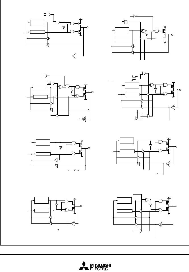
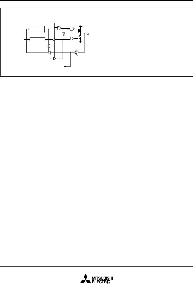
(1) Port P00 |
|
|
Direction |
|
register |
Data bus |
Port latch |
Serial I/O2 input 

(2) Port P01
P01/SOUT2 P-channel output disable bit
Serial I/O2 Transmit completion signal
Serial I/O2 port selection bit
|
Direction |
|
register |
Data bus |
Port latch |
Serial I/O2 output 

(3) Port P02 |
|
|
|
(4) Port P03 |
|
P02/SCLK2 P-channel output disable bit |
|
|
Serial I/O2 synchronous |
SRDY2 output enable bit |
|
|
clock selection bit |
Direction |
Serial I/O2 port selection bit |
||
|
Direction |
register |
|
register |
|
|
Data bus |
Port latch |
Data bus |
Port latch |
|
|
Serial I/O2 ready output |
|
Serial I/O2 clock output |
|
|
|
Serial I/O2 external clock input |
|
(5) Ports P04-P07,P1
|
Direction |
|
register |
Data bus |
Port latch |
(7) Port P21
Port XC switch bit
Direction register
Data bus  Port latch
Sub-clock generating circuit input 
(6) Port P20
Port XC switch bit
Direction register
Data bus  Port latch
Oscillator
Port P21
Port XC switch bit
(8) Ports P22,P23
|
Direction |
|
register |
Data bus |
Port latch |
Fig. 10 Port block diagram (1)
14
|
|
MITSUBISHI MICROCOMPUTERS |
|
|
3850 Group (Spec. H) |
|
|
SINGLE-CHIP 8-BIT CMOS MICROCOMPUTER |
|
|
|
|
|
|
(9) Port P24 |
|
(10) Port P25 |
Serial I/O1 enable bit |
|
|
|
|
|
Receive enable bit |
|
P-channel output disable bit |
|
|
Direction |
Serial I/O1 enable bit |
|
Transmit enable bit |
|
|
register |
|
|
|
|
|
|
Direction |
Data bus |
Port latch |
register |
Data bus 
 Port latch


Serial I/O1 input 
(11) Port P26
Serial I/O1 synchronous clock selection bit 
Serial I/O1 enable bit
Serial I/O1 mode selection bit |
|
Serial I/O1 enable bit |
|
|
Direction |
|
register |
Data bus |
Port latch |
|
Serial I/O1 clock output |
|
External clock input |
(13) Ports P30-P34 |
|
|
Direction |
|
register |
Data bus |
Port latch |
|
A-D converter input |
|
Analog input pin selection bit |
Serial I/O1 output 
(12) Port P27
Pulse output mode
Serial I/O1 mode selection bit
Serial I/O1 enable bit 

SRDY1 output enable bit |
|
|
Direction |
|
register |
Data bus |
Port latch |
Pulse output mode
Serial ready output
Timer output
CNTR0 interrupt  input
input
(14) Port P40 |
|
|
Direction |
|
register |
Data bus |
Port latch |
Pulse output mode Timer output
CNTR1 interrupt input
|
(16) Port P43 |
(15) Ports P41,P42 |
Serial I/O2 I/O |
|
comparison signal control bit |
|
Direction |
|
register |
Data bus |
Port latch |
Direction register
Data bus 
 Port latch
Interrupt input |
|
Serial I/O2 I/O |
|
||
|
|
comparison signal output |
Interrupt input 
Fig. 11 Port block diagram (2)
15
MITSUBISHI MICROCOMPUTERS
3850 Group (Spec. H)
SINGLE-CHIP 8-BIT CMOS MICROCOMPUTER
(17) Port P44 |
|
|
PWM output enable bit |
|
Direction |
|
register |
Data bus |
Port latch |
|
PWM output |
|
Interrupt input |
Fig. 12 Port block diagram (3)
16
Loading...