


 Loading...
Mitsubishi M38279EF-XXXFP, M38277M8MXXXHP, M38277M8MXXXGP, M38277M8MXXXFP, M38279EFHP Datasheet
...MITSUBISHI MICROCOMPUTERS
3827 Group
SINGLE-CHIP 8-BIT CMOS MICROCOMPUTER
DESCRIPTION
The 3827 group is the 8-bit microcomputer based on the 740 family core technology.
The 3827 group has the LCD drive control circuit, the A-D/D-A converter, the UART, and the PWM as additional functions.
The various microcomputers in the 3827 group include variations of internal memory size and packaging. For details, refer to the section on part numbering.
For details on availability of microcomputers in the 3827 group, refer to the section on group expansion.
FEATURES |
|
●Basic machine-language instructions ...................................... |
71 |
●The minimum instruction execution time ........................... |
0.5 μs |
(at 8MHz oscillation frequency) |
|
●Memory size |
|
ROM ................................................................. |
4 K to 60 K bytes |
RAM ................................................................. |
192 to 2048 bytes |
●Programmable input/output ports ............................................ |
55 |
●Output port ................................................................................. |
8 |
●Input port .................................................................................... |
1 |
●Interrupts ................................................. |
17 sources, 16 vectors |
(includes key input interrupt) |
|
●Timers ........................................................... |
8-bit 3, 16-bit 2 |
●Serial I/O1 .................... |
8-bit 1 (UART or Clock-synchronized) |
●Serial I/O2 ................................... |
8-bit 1 (Clock-synchronized) |
●PWM output .................................................................... |
8-bit 1 |
●A-D converter ............................................... |
10-bit 8 channels |
●D-A converter ................................................. |
8-bit 2 channels |
●LCD drive control circuit |
|
Bias ................................................................................... |
1/2, 1/3 |
Duty ........................................................................... |
1/2, 1/3, 1/4 |
Common output .......................................................................... |
4 |
Segment output ........................................................................ |
40 |
●2 Clock generating circuits |
|
(connect to external ceramic resonator or quartz-crystal oscillator)
●Watchdog timer ............................................................ |
14-bit 1 |
●Power source voltage ................................................ |
2.2 to 5.5 V |
●Power dissipation |
|
In high-speed mode .......................................................... |
40 mW |
(at 8 MHz oscillation frequency, at 5 V power source voltage) |
|
In low-speed mode ............................................................ |
60 μW |
(at 32 kHz oscillation frequency, at 3 V power source voltage) |
|
●Operating temperature range ................................... |
– 20 to 85°C |
APPLICATIONS
Camera, wireless phone, etc.
PIN CONFIGURATION (TOP VIEW)
|
|
|
|
|
|
|
|
SEG10 |
SEG11 |
SEG12 |
SEG13 |
SEG14 |
SEG15 |
SEG16 |
SEG17 |
P30/SEG18 |
P31/SEG19 |
P32/SEG20 |
P33/SEG21 |
P34/SEG22 |
P35/SEG23 |
P36/SEG24 |
P37/SEG25 |
P00/SEG26 |
P01/SEG27 |
|
P02/SEG28 |
P03/SEG29 |
P04/SEG30 |
P05/SEG31 |
P06/SEG32 |
P07/SEG33 |
P10/SEG34 |
|
P11/SEG35 |
|
P12/SEG36 |
|
P13/SEG37 |
|
P14/SEG38 |
|
P15/SEG39 |
|
|
|
|
|
|||||||||||||||||||||||||||||||||
|
|
|
|
|
|
|
|
|
|
|
|
|
|
|
|
|
|
|
|
|
|
|
|
|
|
|
|
|
|
|
|
|
|
|
|
|
|
|
|
|
|
|
|
|
|
|
|
|
|
|
|
|
|
|
|
|
|
|
|
|
|
|
|
|
|
|
|
|
|
|
|
|
|
|
|
|
|
|
|
|
|
|
|
|
|
|
|
|
|
|
|
|
|
|
|
|
|
|
|
|
|
|
|
|
|
|
|
|
|
|
|
|
|
|
|
|
|
|
|
|
|
|
|
|
|
|
|
|
|
|
|
|
|
|
|
|
|
|
|
|
|
|
|
|
|
|
|
|
|
|
|
|
|
|
|
|
|
|
|
|
|
|
|
|
|
|
|
|
|
|
|
|
|
|
|
|
|
|
|
|
|
|
|
|
|
|
|
|
|
|
|
|
|
|
|
|
|
|
|
|
|
|
|
|
|
|
|
|
|
|
|
|
|
|
|
|
|
|
|
|
|
|
|
|
|
|
|
|
|
|
|
|
|
|
|
|
|
|
|
|
|
|
|
|
|
|
|
|
|
|
|
|
|
|
|
|
|
|
|
|
|
|
|
|
|
|
|
|
|
|
|
|
|
|
|
|
|
|
|
|
|
|
|
|
|
|
|
|
|
|
|
|
|
|
|
|
|
|
|
|
|
|
|
|
|
|
|
|
|
|
|
|
|
|
|
|
|
|
|
|
|
|
|
|
|
|
|
|
|
|
|
|
|
|
|
80 |
79 |
78 |
77 |
76 |
75 |
74 |
73 |
72 |
71 |
70 |
69 |
68 |
67 |
66 |
65 |
64 |
63 |
62 |
61 |
60 |
59 |
58 |
57 |
56 |
55 |
54 |
53 |
52 |
51 |
|
|
|
|
|
|
|
|
||||||||||||||||||||||||||||||||||||
SEG9 |
|
|
|
81 |
|
|
|
|
|
|
|
|
|
|
|
|
|
|
|
|
|
|
|
|
|
|
|
|
|
|
|
|
|
|
|
|
|
|
|
|
|
|
|
|
|
|
|
|
|
|
|
|
|
|
|
|
|
|
|
|
|
|
|
|
|
|
|
|
|
|
|
|
50 |
|
|
|
P16 |
||||
|
|
|
|
|
|
|
|
|
|
|
|
|
|
|
|
|
|
|
|
|
|
|
|
|
|
|
|
|
|
|
|
|
|
|
|
|
|
|
|
|
|
|
|
|
|
|
|
|
|
|
|
|
|
|
|
|
|
|
|
|
|
|
|
|
|
|
|
|
|
|
|
||||||||||
|
|
|
|
|
|
|
|
|
|
|
|
|
|
|
|
|
|
|
|
|
|
|
|
|
|
|
|
|
|
|
|
|
|
|
|
|
|
|
|
|
|
|
|
|
|
|
|
|
|
|
|
|
|
|
|
|
|
|
|
|
|
|
|
|
|
|
|
|
|
|
|
||||||||||
SEG8 |
|
|
82 |
|
|
|
|
|
|
|
|
|
|
|
|
|
|
|
|
|
|
|
|
|
|
|
|
|
|
|
|
|
|
|
|
|
|
|
|
|
|
|
|
|
|
|
|
|
|
|
|
|
|
|
|
|
|
|
|
|
|
|
|
|
|
|
|
|
|
|
49 |
|
|
|
P17 |
||||||
|
|
|
|
|
|
|
|
|
|
|
|
|
|
|
|
|
|
|
|
|
|
|
|
|
|
|
|
|
|
|
|
|
|
|
|
|
|
|
|
|
|
|
|
|
|
|
|
|
|
|
|
|
|
|
|
|
|
|
|
|
|
|
|
|
|
|
|
|
|
|
|
||||||||||
SEG7 |
|
|
|
|
|
|
|
|
|
|
|
|
|
|
|
|
|
|
|
|
|
|
|
|
|
|
|
|
|
|
|
|
|
|
|
|
|
|
|
|
|
|
|
|
|
|
|
|
|
|
|
|
|
|
|
|
|
|
|
|
|
|
|
|
|
|
|
|
|
|
48 |
|
|
|
P20 |
||||||
|
83 |
|
|
|
|
|
|
|
|
|
|
|
|
|
|
|
|
|
|
|
|
|
|
|
|
|
|
|
|
|
|
|
|
|
|
|
|
|
|
|
|
|
|
|
|
|
|
|
|
|
|
|
|
|
|
|
|
|
|
|
|
|
|
|
|
|
|
|
|
|
|
|
|||||||||
SEG6 |
|
|
|
|
|
|
|
|
|
|
|
|
|
|
|
|
|
|
|
|
|
|
|
|
|
|
|
|
|
|
|
|
|
|
|
|
|
|
|
|
|
|
|
|
|
|
|
|
|
|
|
|
|
|
|
|
|
|
|
|
|
|
|
|
|
|
|
|
|
|
|
47 |
|
|
|
P21 |
|||||
|
84 |
|
|
|
|
|
|
|
|
|
|
|
|
|
|
|
|
|
|
|
|
|
|
|
|
|
|
|
|
|
|
|
|
|
|
|
|
|
|
|
|
|
|
|
|
|
|
|
|
|
|
|
|
|
|
|
|
|
|
|
|
|
|
|
|
|
|
|
|
|
|
|
|||||||||
SEG5 |
|
|
|
|
|
|
|
|
|
|
|
|
|
|
|
|
|
|
|
|
|
|
|
|
|
|
|
|
|
|
|
|
|
|
|
|
|
|
|
|
|
|
|
|
|
|
|
|
|
|
|
|
|
|
|
|
|
|
|
|
|
|
|
|
|
|
|
|
|
|
|
46 |
|
|
|
P22 |
|||||
|
85 |
|
|
|
|
|
|
|
|
|
|
|
|
|
|
|
|
|
|
|
|
|
|
|
|
|
|
|
|
|
|
|
|
|
|
|
|
|
|
|
|
|
|
|
|
|
|
|
|
|
|
|
|
|
|
|
|
|
|
|
|
|
|
|
|
|
|
|
|
|
|
|
|||||||||
SEG4 |
|
|
|
|
|
|
|
|
|
|
|
|
|
|
|
|
|
|
|
|
|
|
|
|
|
|
|
|
|
|
|
|
|
|
|
|
|
|
|
|
|
|
|
|
|
|
|
|
|
|
|
|
|
|
|
|
|
|
|
|
|
|
|
|
|
|
|
|
|
|
|
45 |
|
|
|
P23 |
|||||
|
86 |
|
|
|
|
|
|
|
|
|
|
|
|
|
|
|
|
|
|
|
|
|
|
|
|
|
|
|
|
|
|
|
|
|
|
|
|
|
|
|
|
|
|
|
|
|
|
|
|
|
|
|
|
|
|
|
|
|
|
|
|
|
|
|
|
|
|
|
|
|
|
|
|||||||||
SEG3 |
|
|
|
|
|
|
|
|
|
|
|
|
|
|
|
|
|
|
|
|
|
|
|
|
|
|
|
|
|
|
|
|
|
|
|
|
|
|
|
|
|
|
|
|
|
|
|
|
|
|
|
|
|
|
|
|
|
|
|
|
|
|
|
|
|
|
|
|
|
|
|
44 |
|
|
|
P24 |
|||||
|
87 |
|
|
|
|
|
|
|
|
|
|
|
|
|
|
|
|
|
|
|
|
|
|
|
|
|
|
|
|
|
|
|
|
|
|
|
|
|
|
|
|
|
|
|
|
|
|
|
|
|
|
|
|
|
|
|
|
|
|
|
|
|
|
|
|
|
|
|
|
|
|
|
|||||||||
SEG2 |
|
|
|
|
|
|
|
|
|
|
|
|
|
|
|
|
|
|
|
|
|
|
|
|
|
|
|
|
|
|
|
|
|
|
|
|
|
|
|
|
|
|
|
|
|
|
|
|
|
|
|
|
|
|
|
|
|
|
|
|
|
|
|
|
|
|
|
|
|
|
|
43 |
|
|
|
P25 |
|||||
|
88 |
|
|
|
|
|
|
|
|
|
|
|
|
|
|
|
|
|
|
|
|
|
|
|
|
|
|
|
|
|
|
|
|
|
|
|
|
|
|
|
|
|
|
|
|
|
|
|
|
|
|
|
|
|
|
|
|
|
|
|
|
|
|
|
|
|
|
|
|
|
|
|
|||||||||
SEG1 |
|
|
|
|
|
|
|
|
|
|
|
|
|
|
|
|
|
|
|
|
|
|
|
|
|
|
|
|
|
|
|
|
|
|
|
|
|
|
|
|
|
|
|
|
|
|
|
|
|
|
|
|
|
|
|
|
|
|
|
|
|
|
|
|
|
|
|
|
|
|
|
42 |
|
|
|
P26 |
|||||
|
89 |
|
|
|
|
|
|
|
|
|
|
|
|
|
|
|
|
|
|
|
|
|
M38277M8MXXXFP |
|
|
|
|
|
|
|
|
|
|
|
|
|
|
|
|
|
|
|
|
|
|
|
|
|
|
|
|
|
|||||||||||||||||||||||||||||
SEG0 |
|
|
|
|
|
|
|
|
|
|
|
|
|
|
|
|
|
|
|
|
|
|
|
|
|
|
|
|
|
|
|
|
|
|
|
|
|
|
|
|
|
|
|
|
|
|
|
|
|
|
41 |
|
|
|
P27 |
||||||||||||||||||||||||||
|
90 |
|
|
|
|
|
|
|
|
|
|
|
|
|
|
|
|
|
|
|
|
|
|
|
|
|
|
|
|
|
|
|
|
|
|
|
|
|
|
|
|
|
|
|
|
|
|
|
|
|
|
||||||||||||||||||||||||||||||
VCC |
|
|
|
|
|
|
|
|
|
|
|
|
|
|
|
|
|
|
|
|
|
|
|
|
|
|
|
|
|
|
|
|
|
|
|
|
|
|
|
|
|
|
|
|
|
|
|
|
|
|
|
|
|
|
|
|
|
|
|
|
|
|
|
|
|
|
|
|
|
40 |
|
|
|
VSS |
|||||||
91 |
|
|
|
|
|
|
|
|
|
|
|
|
|
|
|
|
|
|
|
|
|
|
|
|
|
|
|
|
|
|
|
|
|
|
|
|
|
|
|
|
|
|
|
|
|
|
|
|
|
|
|
|
|
|
|
|
|
|
|
|
|
|
|
|
|
|
|
|
|||||||||||||
VREF |
|
|
|
|
|
|
|
|
|
|
|
|
|
|
|
|
|
|
|
|
|
|
|
|
|
|
|
|
|
|
|
|
|
|
|
|
|
|
|
|
|
|
|
|
|
|
|
|
|
|
|
|
|
|
|
|
|
|
|
|
|
|
|
|
|
|
|
|
|
|
|
39 |
|
|
|
XOUT |
|||||
|
92 |
|
|
|
|
|
|
|
|
|
|
|
|
|
|
|
|
|
|
|
|
|
|
|
|
|
|
|
|
|
|
|
|
|
|
|
|
|
|
|
|
|
|
|
|
|
|
|
|
|
|
|
|
|
|
|
|
|
|
|
|
|
|
|
|
|
|
|
|
|
|
|
|||||||||
AVSS |
|
|
|
|
|
|
|
|
|
|
|
|
|
|
|
|
|
|
|
|
|
|
|
|
|
|
|
|
|
|
|
|
|
|
|
|
|
|
|
|
|
|
|
|
|
|
|
|
|
|
|
|
|
|
|
|
|
|
|
|
|
|
|
|
|
|
|
|
|
|
|
38 |
|
|
|
XIN |
|||||
|
93 |
|
|
|
|
|
|
|
|
|
|
|
|
|
|
|
|
|
|
|
|
|
|
|
|
|
|
|
|
|
|
|
|
|
|
|
|
|
|
|
|
|
|
|
|
|
|
|
|
|
|
|
|
|
|
|
|
|
|
|
|
|
|
|
|
|
|
|
|
|
|
|
|||||||||
COM3 |
|
|
|
|
|
|
|
|
|
|
|
|
|
|
|
|
|
|
|
|
|
|
|
|
|
|
|
|
|
|
|
|
|
|
|
|
|
|
|
|
|
|
|
|
|
|
|
|
|
|
|
|
|
|
|
|
|
|
|
|
|
|
|
|
|
|
|
|
|
|
|
|
37 |
|
|
|
XCOUT |
||||
|
|
94 |
|
|
|
|
|
|
|
|
|
|
|
|
|
|
|
|
|
|
|
|
|
|
|
|
|
|
|
|
|
|
|
|
|
|
|
|
|
|
|
|
|
|
|
|
|
|
|
|
|
|
|
|
|
|
|
|
|
|
|
|
|
|
|
|
|
|
|
|
|
|
|
||||||||
COM2 |
|
|
|
|
|
|
|
|
|
|
|
|
|
|
|
|
|
|
|
|
|
|
|
|
|
|
|
|
|
|
|
|
|
|
|
|
|
|
|
|
|
|
|
|
|
|
|
|
|
|
|
|
|
|
|
|
|
|
|
|
|
|
|
|
|
|
|
|
|
|
|
|
36 |
|
|
|
XCIN |
||||
|
|
95 |
|
|
|
|
|
|
|
|
|
|
|
|
|
|
|
|
|
|
|
|
|
|
|
|
|
|
|
|
|
|
|
|
|
|
|
|
|
|
|
|
|
|
|
|
|
|
|
|
|
|
|
|
|
|
|
|
|
|
|
|
|
|
|
|
|
|
|
|
|
|
|
||||||||
COM1 |
|
|
|
|
|
|
|
|
|
|
|
|
|
|
|
|
|
|
|
|
|
|
|
|
|
|
|
|
|
|
|
|
|
|
|
|
|
|
|
|
|
|
|
|
|
|
|
|
|
|
|
|
|
|
|
|
|
|
|
|
|
|
|
|
|
|
|
|
|
|
|
|
|
|
|
|
|
|
|
||
|
|
|
96 |
|
|
|
|
|
|
|
|
|
|
|
|
|
|
|
|
|
|
|
|
|
|
|
|
|
|
|
|
|
|
|
|
|
|
|
|
|
|
|
|
|
|
|
|
|
|
|
|
|
|
|
|
|
|
|
|
|
|
|
|
|
|
|
|
|
|
|
35 |
|
|
|
|
RESET |
|||||
|
|
|
|
|
|
|
|
|
|
|
|
|
|
|
|
|
|
|
|
|
|
|
|
|
|
|
|
|
|
|
|
|
|
|
|
|
|
|
|
|
|
|
|
|
|
|
|
|
|
|
|
|
|
|
|
|
|
|
|
|
|
|
|
|
|
|
|
|
|
||||||||||||
|
|
|
|
|
|
|
|
|
|
|
|
|
|
|
|
|
|
|
|
|
|
|
|
|
|
|
|
|
|
|
|
|
|
|
|
|
|
|
|
|
|
|
|
|
|
|
|
|
|
|
|
|
|
|
|
|
|
|
|
|
|
|
|
|
|
|
|
|
|
|
|
|
|||||||||
COM0 |
|
|
|
|
|
|
|
|
|
|
|
|
|
|
|
|
|
|
|
|
|
|
|
|
|
|
|
|
|
|
|
|
|
|
|
|
|
|
|
|
|
|
|
|
|
|
|
|
|
|
|
|
|
|
|
|
|
|
|
|
|
|
|
|
|
|
|
|
|
|
|
34 |
|
|
|
|
P70/INT0 |
||||
|
97 |
|
|
|
|
|
|
|
|
|
|
|
|
|
|
|
|
|
|
|
|
|
|
|
|
|
|
|
|
|
|
|
|
|
|
|
|
|
|
|
|
|
|
|
|
|
|
|
|
|
|
|
|
|
|
|
|
|
|
|
|
|
|
|
|
|
|
|
|
|
|
|
|||||||||
VL3 |
|
|
|
|
|
|
|
|
|
|
|
|
|
|
|
|
|
|
|
|
|
|
|
|
|
|
|
|
|
|
|
|
|
|
|
|
|
|
|
|
|
|
|
|
|
|
|
|
|
|
|
|
|
|
|
|
|
|
|
|
|
|
|
|
|
|
|
|
|
|
|
33 |
|
|
|
|
P71 |
||||
|
98 |
|
|
|
|
|
|
|
|
|
|
|
|
|
|
|
|
|
|
|
|
|
|
|
|
|
|
|
|
|
|
|
|
|
|
|
|
|
|
|
|
|
|
|
|
|
|
|
|
|
|
|
|
|
|
|
|
|
|
|
|
|
|
|
|
|
|
|
|
|
|
|
|||||||||
VL2 |
|
|
|
|
|
|
|
|
|
|
|
|
|
|
|
|
|
|
|
|
|
|
|
|
|
|
|
|
|
|
|
|
|
|
|
|
|
|
|
|
|
|
|
|
|
|
|
|
|
|
|
|
|
|
|
|
|
|
|
|
|
|
|
|
|
|
|
|
|
|
|
32 |
|
|
|
|
P72 |
||||
|
99 |
|
|
|
|
|
|
|
|
|
|
|
|
|
|
|
|
|
|
|
|
|
|
|
|
|
|
|
|
|
|
|
|
|
|
|
|
|
|
|
|
|
|
|
|
|
|
|
|
|
|
|
|
|
|
|
|
|
|
|
|
|
|
|
|
|
|
|
|
|
|
|
|||||||||
C2 |
|
|
|
|
|
|
|
|
|
|
|
|
|
|
|
|
|
|
|
|
|
|
|
|
|
|
|
|
|
|
|
|
|
|
|
|
|
|
|
|
|
|
|
|
|
|
|
|
|
|
|
|
|
|
|
|
|
|
|
|
|
|
|
|
|
|
|
|
|
|
|
31 |
|
|
|
|
P73 |
||||
|
100 |
|
|
|
|
|
|
|
|
|
|
|
|
|
|
|
|
|
|
|
|
|
|
|
|
|
|
|
|
|
|
|
|
|
|
|
|
|
|
|
|
|
|
|
|
|
|
|
|
|
|
|
|
|
|
|
|
|
|
|
|
|
|
|
|
|
|
|
|
|
|
|
|||||||||
|
|
|
|
|
|
|
|
1 |
2 |
3 |
4 |
5 |
6 |
7 |
8 |
9 |
10 |
11 |
12 |
13 |
14 |
15 |
16 |
17 |
18 |
19 |
20 |
21 |
22 |
23 |
24 |
25 |
|
26 |
|
27 |
|
28 |
|
29 |
|
30 |
|
|
|
|
|
|
|
|
|||||||||||||||||||||||||||||||
|
|
|
|
|
|
|
|
|
|
|
|
|
|
|
|
|
|
|
|
|
|
|
|
|
|
|
|
|
|
|
|
|
|
|
|
|
|
|
|
|
|
|
|
|
|
|
|
|
|
|
|
|
|
|
|
|
|
|
|
|
|
|
|
|
|
|
|
|
|
|
|
|
|
|
|
|
|
|
|
||
|
|
|
|
|
|
|
|
|
|
|
|
|
|
|
|
|
|
|
|
|
|
|
|
|
|
|
|
|
|
|
|
|
|
|
|
|
|
|
|
|
|
|
|
|
|
|
|
|
|
|
|
|
|
|
|
|
|
|
|
|
|
|
|
|
|
|
|
|
|
|
|
|
|
|
|
|
|
|
|
||
|
|
|
|
|
|
|
|
|
|
|
|
|
|
|
|
P65/AN5 |
|
|
|
|
|
|
|
|
|
|
|
|
|
|
|
|
|
|
|
|
|
|
|
|
|
|
|
|
|
|
|
P45/TXD |
P44/RXD |
|
|
|
|
|
|
|
P40/ADT |
|
|
|
|
|
|
|
|
|
|
|
|
|
|
|
|
|
|
|
|
||||
|
|
|
|
|
|
|
|
C1 |
VL1 |
P67/AN7 |
P66/AN6 |
P64/AN4 |
P63/SCLK22/AN3 |
P62/SCLK21/AN2 |
P61/SOUT2/AN1 |
P60/SIN2/AN0 |
P57/DA2 |
P56/DA1 |
P55/CNTR1 |
P54/CNTR0 |
P53/RTP1 |
P52/RTP0 |
P51/PWM1 |
P50/PWM0 |
|
P47/SRDY1 |
P46/SCLK1 |
P43/φ/TOUT |
P42/INT2 |
P41/INT1 |
|
|
P77 |
|
P76 |
|
P75 |
|
P74 |
|
|
|
|
|
|||||||||||||||||||||||||||||||||||||
|
|
|
|
|
|
|
|
|
|
|
|
|
|
|
|
|
|
|
|||||||||||||||||||||||||||||||||||||||||||||||||||||||||||||||
|
|
|
|
|
|
|
|
|
|
|
|
|
|
|
|
|
|
|
|
|
|
|
|
|
|
|
|
|
|
|
|
|
|
||||||||||||||||||||||||||||||||||||||||||||||||
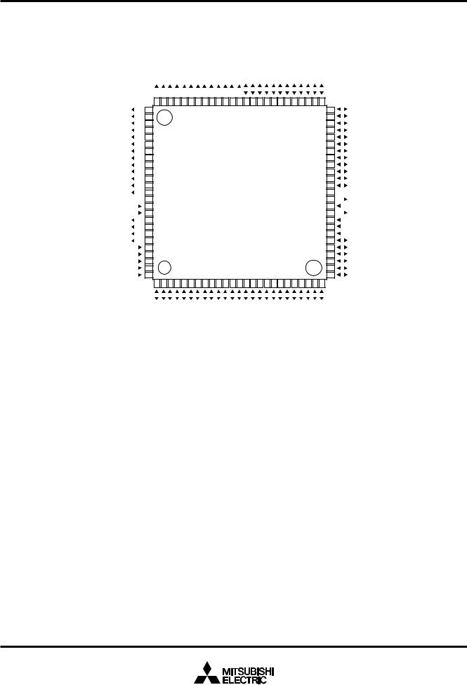
Package type : 100P6S-A (100-pin plastic-molded QFP)
Fig. 1 M38277M8MXXXFP pin configuration
MITSUBISHI MICROCOMPUTERS
3827 Group
SINGLE-CHIP 8-BIT CMOS MICROCOMPUTER
PIN CONFIGURATION (TOP VIEW) |
|
|
|
|
|
|
|
|
|
|
|
|
|
|
|
|
|
|
|
|
|
|
|
|
|
|
|
|
|
|
|
|
|
|
|
|
|
|
|
|
|
|
|
|
|
|
|
|
|
|
|
|||||||||
|
|
|
|
SEG13 |
SEG14 |
SEG15 |
SEG16 |
SEG17 |
P30/SEG18 |
P31/SEG19 |
P32/SEG20 |
P33/SEG21 |
P34/SEG22 |
P35/SEG23 |
P36/SEG24 |
P37/SEG25 |
P00/SEG26 |
P01/SEG27 |
P02/SEG28 |
|
P03/SEG29 |
P04/SEG30 |
P05/SEG31 |
P06/SEG32 |
P07/SEG33 |
P10/SEG34 |
P11/SEG35 |
P12/SEG36 |
P13/SEG37 |
|
|
|
|
|
||||||||||||||||||||||||||
|
|
|
|
|
|
|
|
|
|
|
|
|
|
|
|
|
|
|
|
|
|
|
|
|
|
|
|
|
|
|
|
|
|
|
|
|
|
|
|
|
||||||||||||||||||||
|
|
|
|
|
|
|
|
|
|
|
|
|
|
|
|
|
|
|
|
|
|
|
|
|
|
|
|
|
|
|
|
|
|
|
|
|
|
|
|
|
|
|
|
|
|
|
|
|
|
|
|
|
|
|
|
|
|
|
|
|
|
|
|
|
|
|
|
|
|
|
|
|
|
|
|
|
|
|
|
|
|
|
|
|
|
|
|
|
|
|
|
|
|
|
|
|
|
|
|
|
|
|
|
|
|
|
|
|
|
|
|
|
|
|
|
|
|
|
|
|
|
|
|
75 |
74 |
73 |
72 |
71 |
70 |
69 |
68 |
67 |
66 |
65 |
64 |
63 |
62 |
61 |
60 |
59 |
58 |
57 |
56 |
55 |
54 |
53 |
52 |
51 |
|
|
|
|
|
|
||||||||||||||||||||||||||||
SEG12 |
|
76 |
|
|
|
|
|
|
|
|
|
|
|
|
|
|
|
|
|
|
|
|
|
|
|
|
|
|
|
|
|
|
|
|
|
|
|
|
|
|
|
|
|
|
|
|
|
|
|
|
50 |
|
|
|
|
P14/SEG38 |
||||
|
|
|
|
|
|
|
|
|
|
|
|
|
|
|
|
|
|
|
|
|
|
|
|
|
|
|
|
|
|
|
|
|
|
|
|
|
|
|
|
|
|
|
|
|
|
|
|
|
|
|
|
|
||||||||
SEG11 |
|
77 |
|
|
|
|
|
|
|
|
|
|
|
|
|
|
|
|
|
|
|
|
|
|
|
|
|
|
|
|
|
|
|
|
|
|
|
|
|
|
|
|
|
|
|
|
|
|
|
|
49 |
|
|
|
|
P15/SEG39 |
||||
|
|
|
|
|
|
|
|
|
|
|
|
|
|
|
|
|
|
|
|
|
|
|
|
|
|
|
|
|
|
|
|
|
|
|
|
|
|
|
|
|
|
|
|
|
|
|
|
|
|
|
|
|
||||||||
SEG10 |
|
78 |
|
|
|
|
|
|
|
|
|
|
|
|
|
|
|
|
|
|
|
|
|
|
|
|
|
|
|
|
|
|
|
|
|
|
|
|
|
|
|
|
|
|
|
|
|
|
|
|
48 |
|
|
|
|
P16 |
||||
|
|
|
|
|
|
|
|
|
|
|
|
|
|
|
|
|
|
|
|
|
|
|
|
|
|
|
|
|
|
|
|
|
|
|
|
|
|
|
|
|
|
|
|
|
|
|
|
|
|
|
||||||||||
SEG9 |
|
79 |
|
|
|
|
|
|
|
|
|
|
|
|
|
|
|
|
|
|
|
|
|
|
|
|
|
|
|
|
|
|
|
|
|
|
|
|
|
|
|
|
|
|
|
|
|
|
|
|
47 |
|
|
|
|
P17 |
||||
SEG8 |
|
80 |
|
|
|
|
|
|
|
|
|
|
|
|
|
|
|
|
|
|
|
|
|
|
|
|
|
|
|
|
|
|
|
|
|
|
|
|
|
|
|
|
|
|
|
|
|
|
|
|
46 |
|
|
|
|
P20 |
||||
|
|
|
|
|
|
|
|
|
|
|
|
|
|
|
|
|
|
|
|
|
|
|
|
|
|
|
|
|
|
|
|
|
|
|
|
|
|
|
|
|
|
|
|
|
|
|
|
|
|
|
|
|||||||||
SEG7 |
|
|
81 |
|
|
|
|
|
|
|
|
|
|
|
|
|
|
|
|
|
|
|
|
|
|
|
|
|
|
|
|
|
|
|
|
|
|
|
|
|
|
|
|
|
|
|
|
|
|
|
|
45 |
|
|
|
|
P21 |
|||
|
|
|
|
|
|
|
|
|
|
|
|
|
|
|
|
|
|
|
|
|
|
|
|
|
|
|
|
|
|
|
|
|
|
|
|
|
|
|
|
|
|
|
|
|
|
|
|
|
|
|
|
|
||||||||
SEG6 |
|
|
82 |
|
|
|
|
|
|
|
|
|
|
|
|
|
|
|
|
|
|
|
|
|
|
|
|
|
|
|
|
|
|
|
|
|
|
|
|
|
|
|
|
|
|
|
|
|
|
|
|
44 |
|
|
|
|
P22 |
|||
|
|
|
|
|
|
|
|
|
|
|
|
|
|
|
|
|
|
|
|
|
|
|
|
|
|
|
|
|
|
|
|
|
|
|
|
|
|
|
|
|
|
|
|
|
|
|
|
|
|
|
|
|
||||||||
SEG5 |
|
|
83 |
|
|
|
|
|
|
|
|
|
|
|
|
|
|
|
|
|
|
|
|
|
|
|
|
|
|
|
|
|
|
|
|
|
|
|
|
|
|
|
|
|
|
|
|
|
|
|
|
43 |
|
|
|
|
P23 |
|||
SEG4 |
|
|
84 |
|
|
|
|
|
|
|
|
|
|
|
|
|
|
|
|
|
|
|
|
|
|
|
|
|
|
|
|
|
|
|
|
|
|
|
|
|
|
|
|
|
|
|
|
|
|
|
|
42 |
|
|
|
|
P24 |
|||
SEG3 |
|
|
85 |
|
|
|
|
|
|
|
|
|
|
|
|
|
|
|
|
|
|
|
|
|
|
|
|
|
|
|
|
|
|
|
|
|
|
|
|
|
|
|
|
|
|
|
|
|
|
|
|
41 |
|
|
|
|
P25 |
|||
|
|
|
|
|
|
|
|
|
|
|
|
|
|
|
|
|
|
|
|
|
|
|
|
|
|
|
|
|
|
|
|
|
|
|
|
|
|
|
|
|
|
|
|
|
|
|
|
|
|
|
|
|
||||||||
SEG2 |
|
|
86 |
|
|
|
|
|
|
|
|
|
|
|
|
|
|
|
|
|
|
|
|
|
|
|
|
|
|
|
|
|
|
|
|
|
|
|
|
|
|
|
|
|
|
|
|
|
|
|
|
40 |
|
|
|
|
P26 |
|||
|
|
|
|
|
|
|
|
|
|
|
|
|
|
|
|
|
|
|
|
|
|
|
|
|
|
|
|
|
|
|
|
|
|
|
|
|
|
|
|
|
|
|
|
|
|
|
|
|
|
|
|
|
|
|||||||
SEG1 |
|
|
87 |
|
|
|
|
|
|
|
|
|
|
|
|
|
|
|
|
|
|
|
|
|
|
|
|
|
|
|
|
|
|
|
|
|
|
|
|
|
|
|
|
|
|
|
|
|
|
|
|
39 |
|
|
|
|
P27 |
|||
|
|
|
|
|
|
|
|
|
|
|
|
|
|
|
|
|
|
|
|
|
|
|
|
|
|
|
|
|
|
|
|
|
|
|
|
|
|
|
|
|
|
|
|
|
|
|
|
|
|
|
|
|||||||||
SEG0 |
|
|
88 |
|
|
|
|
|
|
|
|
|
|
|
|
|
M38277M8MXXXGP |
|
|
|
|
|
|
|
|
|
|
|
|
38 |
|
|
|
|
VSS |
|||||||||||||||||||||||||
|
|
|
|
|
|
|
|
|
|
|
|
|
|
|
|
|
|
|
|
|
|
|
|
|
|
|
|
|
|
|||||||||||||||||||||||||||||||
VCC |
89 |
|
|
|
|
|
|
|
|
|
|
|
|
|
|
|
|
|
|
|
|
|
|
|
|
|
|
|
|
|
|
|
|
|
|
|
|
|
|
|
|
|
|
|
|
|
|
|
|
37 |
|
|
|
|
XOUT |
|||||
|
|
|
|
|
|
|
|
|
|
|
|
|
|
|
|
|
|
|
|
|
|
|
|
|
|
|
|
|
|
|
|
|
|
|
|
|
|
|
|
|
|
|
|
|
|
|
|
|
|
|
||||||||||
VREF |
|
|
90 |
|
|
|
|
|
|
|
|
|
|
|
|
|
|
M38277M8MXXXHP |
|
|
|
|
|
|
|
|
|
|
|
|
36 |
|
|
|
|
XIN |
||||||||||||||||||||||||
|
|
|
|
|
|
|
|
|
|
|
|
|
|
|
|
|
|
|
|
|
|
|
|
|
|
|
|
|
|
|
||||||||||||||||||||||||||||||
AVSS |
|
|
91 |
|
|
|
|
|
|
|
|
|
|
|
|
|
|
|
|
|
|
|
|
|
|
|
|
|
|
35 |
|
|
|
|
XCOUT |
|||||||||||||||||||||||||
|
|
|
|
|
|
|
|
|
|
|
|
|
|
|
|
|
|
|
|
|
|
|
|
|
|
|
|
|
|
|
|
|
|
|
|
|
|
|
|
|
|
|
|
|
|
|
|
|
|
|
|
|
|
|||||||
COM3 |
|
92 |
|
|
|
|
|
|
|
|
|
|
|
|
|
|
|
|
|
|
|
|
|
|
|
|
|
|
|
|
|
|
|
|
|
|
|
|
|
|
|
|
|
|
|
|
|
|
|
|
34 |
|
|
|
|
XCIN |
||||
|
|
|
|
|
|
|
|
|
|
|
|
|
|
|
|
|
|
|
|
|
|
|
|
|
|
|
|
|
|
|
|
|
|
|
|
|
|
|
|
|
|
|
|
|
|
|
|
|
|
|
|
|||||||||
COM2 |
|
93 |
|
|
|
|
|
|
|
|
|
|
|
|
|
|
|
|
|
|
|
|
|
|
|
|
|
|
|
|
|
|
|
|
|
|
|
|
|
|
|
|
|
|
|
|
|
|
|
|
33 |
|
|
|
|
RESET |
|
|||
|
|
|
|
|
|
|
|
|
|
|
|
|
|
|
|
|
|
|
|
|
|
|
|
|
|
|
|
|
|
|
|
|
|
|
|
|
|
|
|
|
|
|
|
|
|
|
|
|
|
|
|
|||||||||
COM1 |
|
94 |
|
|
|
|
|
|
|
|
|
|
|
|
|
|
|
|
|
|
|
|
|
|
|
|
|
|
|
|
|
|
|
|
|
|
|
|
|
|
|
|
|
|
|
|
|
|
|
|
32 |
|
|
|
|
P70/INT0 |
||||
|
|
|
|
|
|
|
|
|
|
|
|
|
|
|
|
|
|
|
|
|
|
|
|
|
|
|
|
|
|
|
|
|
|
|
|
|
|
|
|
|
|
|
|
|
|
|
|
|
|
|
|
|||||||||
COM0 |
|
95 |
|
|
|
|
|
|
|
|
|
|
|
|
|
|
|
|
|
|
|
|
|
|
|
|
|
|
|
|
|
|
|
|
|
|
|
|
|
|
|
|
|
|
|
|
|
|
|
|
31 |
|
|
|
|
P71 |
||||
VL3 |
|
|
96 |
|
|
|
|
|
|
|
|
|
|
|
|
|
|
|
|
|
|
|
|
|
|
|
|
|
|
|
|
|
|
|
|
|
|
|
|
|
|
|
|
|
|
|
|
|
|
|
|
30 |
|
|
|
|
P72 |
|||
|
|
|
|
|
|
|
|
|
|
|
|
|
|
|
|
|
|
|
|
|
|
|
|
|
|
|
|
|
|
|
|
|
|
|
|
|
|
|
|
|
|
|
|
|
|
|
|
|
|
|
|
|
||||||||
VL2 |
|
|
97 |
|
|
|
|
|
|
|
|
|
|
|
|
|
|
|
|
|
|
|
|
|
|
|
|
|
|
|
|
|
|
|
|
|
|
|
|
|
|
|
|
|
|
|
|
|
|
|
|
29 |
|
|
|
|
P73 |
|||
|
|
|
|
|
|
|
|
|
|
|
|
|
|
|
|
|
|
|
|
|
|
|
|
|
|
|
|
|
|
|
|
|
|
|
|
|
|
|
|
|
|
|
|
|
|
|
|
|
|
|
|
|
||||||||
C2 |
|
|
98 |
|
|
|
|
|
|
|
|
|
|
|
|
|
|
|
|
|
|
|
|
|
|
|
|
|
|
|
|
|
|
|
|
|
|
|
|
|
|
|
|
|
|
|
|
|
|
|
|
28 |
|
|
|
|
P74 |
|||
|
|
|
|
|
|
|
|
|
|
|
|
|
|
|
|
|
|
|
|
|
|
|
|
|
|
|
|
|
|
|
|
|
|
|
|
|
|
|
|
|
|
|
|
|
|
|
|
|
|
|
|
|
||||||||
C1 |
|
|
99 |
|
|
|
|
|
|
|
|
|
|
|
|
|
|
|
|
|
|
|
|
|
|
|
|
|
|
|
|
|
|
|
|
|
|
|
|
|
|
|
|
|
|
|
|
|
|
|
|
27 |
|
|
|
|
P75 |
|||
VL1 |
|
|
100 |
|
|
|
|
|
|
|
|
|
|
|
|
|
|
|
|
|
|
|
|
|
|
|
|
|
|
|
|
|
|
|
|
|
|
|
|
|
|
|
|
21 |
|
|
23 |
24 |
26 |
|
|
|
|
P76 |
||||||
|
|
|
|
|
|
|
|
|
|
|
|
|
|
|
|
|
|
|
|
|
|
|
|
|
|
|
|
|
|
|
|
|
|
|
|
|
|
|
|
|
|
|
|
|
|
|
||||||||||||||
|
|
1 |
2 |
3 |
4 |
5 |
6 |
7 |
8 |
9 |
10 |
11 |
12 |
13 |
14 |
15 |
16 |
17 |
18 |
19 |
20 |
22 |
25 |
|
|
|
|
|
|
|||||||||||||||||||||||||||||||
|
|
|
|
|
|
|
|
|
|
|
|
|
|
|
|
|
|
|
|
|
|
|
|
|
|
|
|
|
|
|
|
|
|
|
|
|
|
|
|
|
|
|
|
|
|
|
|
|
|
|
|
|
|
|
|
|
|
|||
|
|
|
|
|
|
|
|
|
|
|
|
|
|
|
|
|
|
|
|
|
|
|
|
|
|
|
|
|
|
|
|
|
|
|
|
|
|
|
|
|
|
|
|
|
|
|
|
|
|
|
|
|
|
|
|
|
|
|
||
|
|
|
|
P67/AN7 |
P66/AN6 |
P65/AN5 |
P64/AN4 |
P63/SCLK22 /AN3 |
P62/SCLK21/AN2 |
P61/SOUT2 /AN1 |
P60/SIN2/AN0 |
P57/DA2 |
P56/DA1 |
P55/CNTR1 |
P54/CNTR0 |
P53/RTP1 |
P52/RTP0 |
P51/PWM1 |
P50/PWM0 |
|
P47/SRDY1 |
P46/SCLK1 P45/ TXD |
P44/RXD P43/φ/TOUT |
P42/INT2 |
P41/INT1 |
P40/ADT |
P77 |
|
|
|
|
|
||||||||||||||||||||||||||||
|
|
|
|
|
|
|
|
|||||||||||||||||||||||||||||||||||||||||||||||||||||
|
|
|
|
|
|
|
|
|
|
|
||||||||||||||||||||||||||||||||||||||||||||||||||
Package type : GP........ 100P6Q-A (100-pin plastic-molded LQFP) |
||||||||||||||||||||||||||||||||||||||||||||||||||||||||||||
Package type : HP ........ 100PFB-A (100-pin plastic-molded TQFP) |
||||||||||||||||||||||||||||||||||||||||||||||||||||||||||||
|
|
|
|
|
|
|
|
|
|
|
|
|
|
|
|
|
|
|
|
|
|
|
|
|
|
|
|
|
|
|
|
|
|
|||||||||||||||||||||||||||
Fig. 2 M38277M8MXXXGP/M38277M8MXXXHP pin configuration |
|
|
|
|
|
|
|
|
|
|
|
|
|
|
|
|
|
|
|
|
|
|
|
|
|
|
|
|
|
|
|
|
|
|||||||||||||||||||||||||||
2

.Fig |
FUNCTIONAL BLOCK DIAGRAM |
|
|
|
|
|
|
|
|
|
|
|
|
|
|||||
3 |
|
|
|
|
|
|
|
|
|
|
|
|
|
|
|
|
|
|
|
Functional |
|
|
|
|
|
|
|
|
|
|
|
|
|
|
|
|
|
|
|
block |
|
Main clock input |
Main clock output |
|
|
Reset input |
( 5 V ) |
( 0 V ) |
|
|
|
|
|
|
|
|
|
|
|
|
|
|
|
|
|
|
|
|
|
|
|
|
|
||||||
diagram |
|
X IN |
X OUT |
|
|
|
RESET |
VCC |
VSS |
|
|
|
|
|
|
|
|
|
|
|
|
|
|
|
|
|
|
Data bus |
|
|
|
|
|
|
|
|
|
|
|
|
|
|
|
|
|
|
|
|
|
|
|
|
|
|
|
|
|
|
|
|
|
|
|
|
|
|
|
|
|
|
|
|
|
|
|
VL1 |
|
|
|
|
|
Clock generating circuit |
|
|
|
|
|
|
|
|
|
|
|
C1 |
|
|
|
||
|
|
|
|
|
|
|
|
|
|
|
|
|
C2 |
|
|
|
|||
|
|
|
|
|
|
|
|
|
|
|
|
|
|
|
|
VL2 |
|
|
|
|
|
|
|
|
|
|
|
|
|
|
|
|
|
|
|
VL3 |
|
|
|
|
|
|
X COUT |
φ |
|
|
|
|
|
|
|
|
|
|
|
COM0 |
|
|
|
|
|
X CIN |
|
|
|
|
|
|
|
|
|
LCD drive |
|
COM1 |
|
|
|
||
|
|
Sub-clock input |
|
|
|
|
|
|
|
|
|
|
|
|
COM2 |
|
|
|
|
|
|
|
|
|
|
|
|
|
|
|
|
|
|
control circuit |
|
|
|
|
|
|
|
Sub-clock output |
|
|
|
|
|
|
|
|
|
|
|
COM3 |
|
|
|
||
|
|
|
|
|
|
|
|
|
|
|
|
|
|
|
|
|
|||
|
|
|
|
|
|
|
|
|
|
Timer X(16) |
|
|
|
|
SEG0 |
|
|
|
|
|
|
|
|
Reset |
|
|
|
|
|
Timer Y(16) |
|
|
|
|
SEG1 |
|
|
|
|
|
|
Watchdog timer |
|
|
|
|
|
D-A2 |
D-A1 |
|
|
SEG2 |
|
|
|
||||
|
|
|
|
|
|
|
|
|
Timer 1(8) |
Timer 2(8) |
|
|
|
|
SEG3 |
|
|
|
|
|
|
|
|
|
|
|
|
|
|
|
|
|
SEG4 |
|
|
|
|||
|
|
|
|
|
|
|
|
|
|
|
Timer 3(8) |
|
|
|
|
|
|
|
|
|
|
|
|
|
|
|
|
|
|
|
|
|
|
|
SEG5 |
|
|
|
|
|
|
|
|
|
|
|
|
|
|
|
|
|
|
|
|
|
|
|
|
|
|
|
|
|
|
|
|
|
|
|
|
|
|
|
|
SEG6 |
|
|
|
|
|
|
|
|
|
|
|
|
|
|
|
|
|
|
|
SEG7 |
|
|
|
|
|
|
|
|
|
|
|
|
|
|
|
|
|
|
|
SEG8 |
|
|
|
|
|
|
|
|
|
|
|
|
|
|
|
function |
|
|
|
SEG9 |
|
|
|
|
|
|
|
|
|
|
|
|
|
|
|
|
|
|
SEG10 |
|
|
|
|
|
|
|
|
|
|
|
|
|
|
|
|
|
|
|
|
SEG11 |
|
|
|
|
|
|
|
|
|
|
DA1 |
|
|
|
|
porttimeReal |
|
|
|
SEG12 |
SINGLE |
|
|
|
|
|
|
|
|
|
|
|
|
|
|
|
|
SEG13 |
|
|
|||
|
|
|
|
|
|
A-D converter |
|
PWM(8) |
SI/O1 (8) |
|
|
|
|
|
SEG14 |
|
|
|
|
|
|
|
|
|
|
|
|
|
|
|
|
SEG15 |
|
|
|
||||
|
|
|
|
|
|
(10) |
|
|
|
|
TOUT |
|
|
|
|
SEG16 |
|
|
|
|
|
|
|
|
|
|
DA2 |
|
|
|
|
|
|
|
|
|
|
||
|
|
|
|
|
|
|
|
|
|
|
|
|
|
|
SEG17 |
|
|
|
|
|
|
|
|
|
|
|
|
|
|
|
|
|
|
|
|
|
|
|
|
|
|
|
|
|
|
|
|
|
|
|
|
|
|
|
|
|
- |
|
|
|
|
|
|
INT0 |
SI/O2(8) |
|
CNTR0,CNTR1 |
|
|
INTINT21, |
|
|
interruptup-wakeon-input/keyKey |
|
|
|
MICROCOMPUTERCMOSBIT-8CHIP |
Group3827 |
MICROCOMPUTERSMITSUBISHI |
3 |
|
|
|
|
|
ADT |
|
|
|
|
|
|
|
||||||
|
|
P7(8) |
|
P6(8) |
|
P5(8) |
|
P4(8) |
|
P3(8) |
P2(8) |
P1(8) |
|
P0(8) |
|
|
|
|
|
|
X COUT |
|
|
|
|
|
|
φ |
|
|
|
|
|
|
|
|
|
|
|
|
X CIN |
|
|
|
|
|
|
|
|
|
|
|
|
|
|
|
|
|
|
|
XCIN XCOUT |
|
I/O port P6 |
VREF |
I/O port P5 |
|
I/O port P4 |
|
Output port P3 |
I/O port P2 |
I/O port P1 |
|
I/O port P0 |
|
|
|
|
||
|
Sub-clock input |
I/O port P7 |
|
|
|
|
|
|
|
||||||||||
|
Sub-clock output |
|
|
|
AVSS |
|
|
|
|
|
|
|
|
|
|
|
|
|
|
|
|
|
|
|
|
|
|
|
|
|
|
|
|
|
|
|
|
||

|
|
|
|
|
MITSUBISHI MICROCOMPUTERS |
||
|
|
|
|
|
|
3827 Group |
|
|
|
|
|
SINGLE-CHIP 8-BIT CMOS MICROCOMPUTER |
|||
|
|
|
|
|
|
|
|
PIN DESCRIPTION |
|
|
|
||||
Table 1 Pin description (1) |
|
|
|
||||
|
|
|
|
|
|
|
|
|
Pin |
Name |
Function |
|
|
||
|
Function except a port function |
||||||
|
|
|
|
|
|
||
|
|
|
|
|
|
|
|
VCC, VSS |
Power source |
•Apply voltage of 2.2 V to 5.5 V to VCC, and 0 V to VSS. |
|
|
|||
|
|
|
|
|
|
||
VREF |
Analog refer- |
•Reference voltage input pin for A-D converter and D-A converter. |
|||||
|
|
|
ence voltage |
|
|
|
|
|
|
|
|
|
|
|
|
AVSS |
Analog power |
•GND input pin for A-D converter and D-A converter. |
|
|
|||
|
|
|
source |
•Connect to VSS. |
|
|
|
|
|
|
|
|
|
||
|
|
|
|
|
|
|
|
|
|
|
Reset input |
•Reset input pin for active “L”. |
|
|
|
RESET |
|
|
|||||
XIN |
Clock input |
•Input and output pins for the main clock generating circuit. |
|||||
|
|
|
|
•Connect a ceramic resonator or a quartz-crystal oscillator between the XIN and XOUT pins to set |
|||
|
|
|
|
the oscillation frequency. |
|
|
|
XOUT |
Clock output |
|
|
||||
•If an external clock is used, connect the clock source to the XIN pin and leave the XOUT pin open. |
|||||||
|
|
|
|
||||
|
|
|
|
|
|
|
|
VL1–VL3 |
LCD power |
•Input 0 ≤ VL1 ≤ VL2 ≤ VL3 ≤ VCC voltage. |
|
|
|||
|
|
|
source |
•Input 0 – VL3 voltage to LCD. |
|
|
|
|
|
|
|
|
|
||
|
|
|
|
|
|
||
C1, C2 |
Charge-pump |
•External capacitor pins for a voltage multiplier (3 times) of LCD contorl. |
|||||
|
|
|
capacitor pin |
|
|
|
|
|
|
|
|
|
|
|
|
COM0–COM3 |
Common output |
•LCD common output pins. |
|
|
|||
|
|
|
|
•COM2 and COM3 are not used at 1/2 duty ratio. |
|
|
|
|
|
|
|
•COM3 is not used at 1/3 duty ratio. |
|
|
|
|
|
|
|
|
|
|
|
SEG0–SEG17 |
Segment output |
•LCD segment output pins. |
|
|
|||
|
|
|
|
|
|
|
|
P00/SEG26– |
I/O port P0 |
•8-bit output port. |
|
•LCD segment output pins |
|||
P07/SEG33 |
|
•CMOS compatible input level. |
|
|
|||
|
|
|
|
|
|
||
|
|
|
|
•CMOS 3-state output structure. |
|
|
|
|
|
|
|
•Pull-up control is enabled. |
|
|
|
|
|
|
|
•I/O direction register allows each port to be individually |
|
|
|
|
|
|
|
programmed as either input or output. |
|
|
|
|
|
|
|
|
|||
P10/SEG34– |
I/O port P1 |
•6-bit output port with same function as port P0. |
|
|
|||
P15/SEG39 |
|
•CMOS compatible input level. |
|
|
|||
|
|
|
|
|
|
||
|
|
|
|
•CMOS 3-state output structure. |
|
|
|
|
|
|
|
•Pull-up control is enabled. |
|
|
|
|
|
|
|
•I/O direction register allows each 6-bit pin to be pro- |
|
|
|
|
|
|
|
grammed as either input or output. |
|
|
|
|
|
|
|
|
|
|
|
P16, P17 |
|
•2-bit I/O port. |
|
|
|||
|
|
|
|
•CMOS compatible input level. |
|
|
|
|
|
|
|
•CMOS 3-state output structure. |
|
|
|
|
|
|
|
•I/O direction register allows each pin to be individually programmed as either input or output. |
|||
|
|
|
|
•Pull-up control is enabled. |
|
|
|
P20 – P27 |
I/O port P2 |
•8-bit I/O port with same function as port P0. |
|
•Key input (key-on wake-up) interrupt |
|||
|
|
|
|
•CMOS compatible input level. |
|
input pins |
|
|
|
|
|
|
|
||
|
|
|
|
•CMOS 3-state output structure. |
|
|
|
|
|
|
|
•Pull-up control is enabled. |
|
|
|
|
|
|
|
|
|
|
|
P30/SEG18 – |
Output port P3 |
•8-bit output port with same function as port P0. |
|
•LCD segment output pins |
|||
P37/SEG25 |
|
•CMOS 3-state output structure. |
|
|
|||
|
|
|
|
|
|
||
|
|
|
|
•Port output control is enabled. |
|
|
|
4

MITSUBISHI MICROCOMPUTERS
3827 Group
SINGLE-CHIP 8-BIT CMOS MICROCOMPUTER
Table 2 Pin description (2)
|
Pin |
Name |
Function |
|
|
|
|
|
|
Function except a port function |
|||
|
|
|
|
|
|
|
|
|
|
|
|
||
P40 |
/ADT |
I/O port P4 |
•1-bit I/O port with same function as P16 and P17. |
•A-D trigger input pin |
||
|
|
|
•CMOS compatible input level. |
•Interrupt input pin |
||
|
|
|
•CMOS 3-state output structure. |
|
|
|
|
|
|
|
|
||
P41 |
/INT1, |
|
•7-bit I/O port with same function as P16 and P17. |
•Interrupt input pins |
||
P42 |
/INT2 |
|
•CMOS compatible input level. |
|
|
|
|
|
|
|
|
|
|
|
|
|
•CMOS 3-state output structure. |
|
|
|
|
φ |
|
• |
φ |
clock output pin |
|
P43/ /TOUT |
|
|
|
|||
|
|
|
•Pull-up control is enabled. |
•Timer 2 output pin |
||
|
|
|
|
|
||
P44 |
/RXD, |
|
|
•Serial I/O1 I/O pins |
||
P45 |
/TXD, |
|
|
|
|
|
P46 |
/SCLK1, |
|
|
|
|
|
P47 |
/SRDY1 |
|
|
|
|
|
P50 |
/PWM0, |
I/O port P5 |
•8-bit I/O port with same function as P16 and P17. |
•PWM function pins |
||
P51 |
/PWM1 |
|
•CMOS compatible input level. |
|
|
|
|
|
|
|
|
|
|
|
|
|
•CMOS 3-state output structure. |
|
||
P52 |
/RTP0, |
|
•Real time port function pins |
|||
P53 |
/RTP1 |
|
•Pull-up control is enabled. |
|
|
|
|
|
|
|
|
||
P54 |
/CNTR0, |
|
|
•Timer X, Y function pins |
||
P55 |
/CNTR1 |
|
|
|
|
|
|
|
|
|
|
||
P56 |
/DA1, |
|
|
•D-A conversion output pins |
||
P57 |
/DA2 |
|
|
|
|
|
|
|
|
|
|||
P60/AN0/SIN2, |
I/O port P6 |
•8-bit I/O port with same function as P16 and P17. |
•A-D conversion input pins |
|||
P61/AN1/SOUT2, |
|
•CMOS compatible input level. |
•Serial I/O2 I/O pins |
|||
P62/AN2/SCLK21, |
|
|||||
|
•CMOS 3-state output structure. |
|
|
|
||
P63/AN3/SCLK22 |
|
|
|
|
||
|
|
|
|
|
||
|
|
|
•Pull-up control is enabled. |
|
|
|
P64 |
/AN4– |
|
|
•A-D conversion input pins |
||
P67 |
/AN7 |
|
|
|
|
|
|
|
|
|
|
||
P70 |
/INT0 |
Input port P7 |
•1-bit I/O port. |
•Interrupt input pin |
||
|
|
|
•CMOS compatible input level. |
|
|
|
|
|
|
|
|
|
|
P71 |
–P77 |
I/O port P7 |
•7-bit I/O port with same function as P16 and P17. |
|
|
|
|
|
|
•CMOS compatible input level. |
|
|
|
|
|
|
•N-channel open-drain output structure. |
|
|
|
|
|
|
|
|
|
|
XCOUT |
Sub-clock output |
•Sub-clock generating circuit I/O pins. |
|
|
|
|
|
|
(Connect a resonator. External clock cannot be used.) |
|
|
|
|
XCIN |
Sub-clock input |
|
|
|
||
|
|
|
|
|
|
|
5
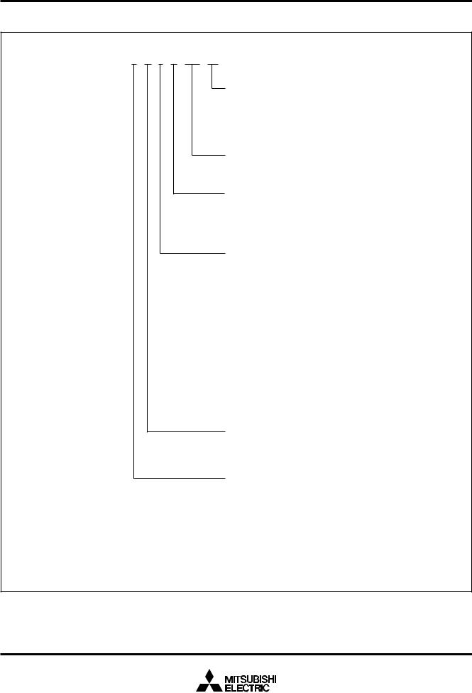
MITSUBISHI MICROCOMPUTERS
3827 Group
SINGLE-CHIP 8-BIT CMOS MICROCOMPUTER
PART NUMBERING
Product M3827 7 M 8 M XXX HP
Package type
FP : 100P6S-A package
HP : 100PFB-A package
GP : 100P6Q-A package
FS : 100D0 package
ROM number
Omitted in some types.
Normally, using hyphen
When electrical characteristic, or division of quality identification code using alphanumeric character.
– : Standard
M : Low power source version
ROM/PROM size
1: 4096 bytes
2: 8192 bytes
3: 12288 bytes
4: 16384 bytes
5: 20480 bytes
6: 24576 bytes
7: 28672 bytes
8: 32768 bytes
9: 36864 bytes A : 40960 bytes B : 45056 bytes C : 49152 bytes D : 53248 bytes E : 57344 bytes F : 61440 bytes
The first 128 bytes and the last 2 bytes of ROM are reserved areas ; they cannot be used.
Memory type
M : Mask ROM version
E : EPROM or One Time PROM version
RAM size
0: 192 bytes
1: 256 bytes
2: 384 bytes
3: 512 bytes
4: 640 bytes
5: 768 bytes
6: 896 bytes
7: 1024 bytes
8: 1536 bytes
9: 2048 bytes
Fig. 4 Part numbering
6

|
|
|
|
|
|
|
|
|
|
|
|
|
|
MITSUBISHI MICROCOMPUTERS |
|||||||
|
|
|
|
|
|
|
|
|
|
|
|
|
|
|
|
|
|
3827 Group |
|||
|
|
|
|
|
|
|
|
|
|
|
SINGLE-CHIP 8-BIT CMOS MICROCOMPUTER |
||||||||||
|
|
|
|
|
|
|
|
|
|
|
|
|
|
|
|
|
|
|
|
|
|
GROUP EXPANSION |
|
|
|
|
|
|
|
Package |
|
|
|
|
|
|
|
|
|
|
|||
Mitsubishi plans to expand the 3827 group as follows: |
|
|
|
|
100PFB-A ................................ |
|
|
|
|
0.4 mm-pitch plastic molded TQFP |
|||||||||||
Memory Type |
|
|
|
|
|
|
|
100P6Q-A ................................ |
|
|
|
|
0.5 mm-pitch plastic molded LQFP |
||||||||
|
|
|
|
|
|
|
100P6S-A ................................ |
|
|
|
|
0.65 mm-pitch plastic molded QFP |
|||||||||
Support for Mask ROM, One Time PROM, and EPROM versions |
|
|
100D0 |
..................... |
|
|
Window type ceramic LCC (EPROM version) |
||||||||||||||
Memory Size |
|
|
|
|
|
|
|
|
|
|
|
|
|
|
|
|
|
|
|
||
ROM/PROM size ................................................. |
|
|
4 K to 60 K bytes |
|
|
|
|
|
|
|
|
|
|
|
|
||||||
RAM size ............................................................ |
|
|
192 to 2048 bytes |
|
|
|
|
|
|
|
|
|
|
|
|
||||||
|
|
|
|
|
|
|
|
|
|
|
|
|
|
|
|
|
|
|
|
|
|
Memory Expansion Plan |
|
|
|
|
|
|
|
|
|
|
|
|
|
|
|
|
|
|
|
||
ROM size (bytes) |
|
|
|
|
|
|
|
|
|
|
|
|
|
|
|
|
|
|
|
||
|
|
|
|
|
|
|
|
|
|
|
|
|
|
Under development |
|
|
|||||
|
|
|
|
|
|
|
|
|
|
|
|
|
|
|
|
|
|
||||
60K |
|
|
|
|
|
|
|
|
|
|
|
|
|
|
|
|
|
|
M38279EF |
||
|
|
|
|
|
|
|
|
|
|
|
|
|
|
|
|
|
|||||
56K |
|
|
|
|
|
|
|
|
|
|
|
|
|
|
|
|
|
|
|
|
|
52K |
|
|
|
|
|
|
|
|
|
|
|
|
|
|
|
|
|
|
|
|
|
|
|
|
|
|
|
|
|
|
|
|
|
Planning |
|
|
|
|
|
|
|
|
|
48K |
|
|
|
|
|
|
|
|
|
|
|
|
M38278MCM |
|
|
|
|
|
|
|
|
44K |
|
|
|
|
|
|
|
|
|
|
|
|
|
|
|
|
|
|
|
|
|
40K |
|
|
|
|
|
|
|
|
|
|
|
|
|
|
|
|
|
|
|
|
|
36K |
|
|
|
|
|
|
|
|
|
|
|
|
|
|
|
|
|
|
|
|
|
|
|
|
|
|
|
Under development |
|
|
|
|
|
|
|
|
|
|
|
|
|
||
32K |
|
|
|
|
|
|
|
M38277M8M |
|
|
|
|
|
|
|
|
|
|
|
||
28K |
|
|
|
|
|
|
|
|
|
|
|
|
|
|
|
|
|
|
|
|
|
24K |
|
|
|
|
|
|
|
|
|
|
|
|
|
|
|
|
|
|
|
|
|
20K |
|
|
|
|
|
|
|
|
|
|
|
|
|
|
|
|
|
|
|
|
|
16K |
|
|
|
|
|
|
|
|
|
|
|
|
|
|
|
|
|
|
|
|
|
12K |
|
|
|
|
|
|
|
|
|
|
|
|
|
|
|
|
|
|
|
|
|
8K |
|
|
|
|
|
|
|
|
|
|
|
|
|
|
|
|
|
|
|
|
|
4K |
|
|
|
|
|
|
|
|
|
|
|
|
|
|
|
|
|
|
|
|
|
|
|
|
|
|
|
|
|
|
|
|
|
|
|
|
|
|
|
|
|
|
|
192 256 |
384 |
512 |
640 |
768 |
896 |
1024 |
1152 |
1280 |
1408 |
1536 |
1664 |
1792 |
1920 |
2048 |
|||||||
|
|
|
|
|
|
|
|
RAM size (bytes) |
|
|
|
|
|
|
|
|
|
|
|
||
Note: Products under development or planning: the development schedule and specifications may be revised without notice.
Fig. 5 Memory expansion plan
Currently supported products are listed below.
Table 3 List of supported products |
|
|
|
As of May 1998 |
||
|
Product |
(P) ROM size (bytes) |
|
RAM size (bytes) |
Package |
Remarks |
|
ROM size for User in ( |
) |
||||
|
|
|
|
|
||
|
|
|
|
|
|
|
|
M38277M8MXXXFP |
32768 |
|
|
100P6S-A |
Mask ROM version |
|
M38277M8MXXXHP |
|
1024 |
100PFB-A |
Mask ROM version |
|
|
(32638) |
|
||||
|
M38277M8MXXXGP |
|
|
100P6Q-A |
Mask ROM version |
|
|
|
|
|
|||
|
M38279EF-XXXFP |
|
|
|
100P6S-A |
One Time PROM version |
|
M38279EFFP |
|
|
|
100P6S-A |
One Time PROM version (blank) |
|
M38279EF-XXXHP |
61440 |
|
|
100PFB-A |
One Time PROM version |
|
M38279EFHP |
|
2048 |
100PFB-A |
One Time PROM version (blank) |
|
|
(61310) |
|
||||
|
M38279EF-XXXGP |
|
|
100P6Q-A |
One Time PROM version |
|
|
|
|
|
|||
|
M38279EFGP |
|
|
|
100P6Q-A |
One Time PROM version (blank) |
|
M38279EFFS |
|
|
|
100D0 |
EPROM version |
|
|
|
|
|
|
|
7
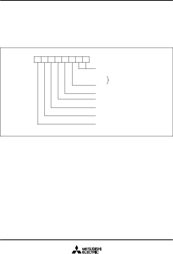
MITSUBISHI MICROCOMPUTERS
3827 Group
SINGLE-CHIP 8-BIT CMOS MICROCOMPUTER
FUNCTIONAL DESCRIPTION
Central Processing Unit (CPU)
The 3827 group uses the standard 740 family instruction set. Refer to the table of 740 family addressing modes and machine instructions or the 740 Family Software Manual for details on the instruction set.
Machine-resident 740 family instructions are as follows:
The FST and SLW instruction cannot be used.
The STP, WIT, MUL, and DIV instruction can be used.
[CPU Mode Register (CPUM)] 003B16
The CPU mode register contains the stack page selection bit and the internal system clock selection bit.
The CPU mode register is allocated at address 003B16.
b7 |
b0 |
CPU mode register
(CPUM (CM) : address 003B16)
Processor mode bits
b1 b0 |
|
|
0 |
0 |
: Single-chip mode |
0 |
1 |
: |
1 |
0 |
: Not available |
1 |
1 |
: |
Stack page selection bit |
||
0 |
: 0 page |
|
1 |
: 1 page |
|
Not used (returns “1” when read) |
||
(Do not write “0” to this bit.) |
||
Port XC switch bit |
||
0 |
: Stop oscillating |
|
1 |
: XCIN, XCOUT |
|
Main clock ( XIN-XOUT) stop bit |
||
0 |
: Oscillating |
|
1 |
: Stopped |
|
Main clock division ratio selection bit |
||
0 |
: XIN/2 (high-speed mode) |
|
1 |
: XIN/8 (middle-speed mode) |
|
Internal system clock selection bit |
||
0 |
: XIN-XOUT selected (middle-/high-speed mode) |
|
1 |
: XCIN-XCOUT selected (low-speed mode) |
|
Fig. 6 Structure of CPU mode register
8
|
|
|
|
|
|
|
|
|
|
|
|
|
|
MITSUBISHI MICROCOMPUTERS |
|||||
|
|
|
|
|
|
|
|
|
|
|
|
|
|
|
3827 Group |
||||
|
|
|
|
|
|
|
|
|
|
|
|
SINGLE-CHIP 8-BIT CMOS MICROCOMPUTER |
|||||||
|
|
|
|
|
|
|
|
|
|
|
|
|
|
|
|
|
|
|
|
MEMORY |
|
|
|
|
|
Zero Page |
|
|
|
|
|
|
|||||||
Special Function Register (SFR) Area |
Access to this area with only 2 bytes is possible in the zero page |
||||||||||||||||||
The Special Function Register area in the zero page contains con- |
addressing mode. |
|
|
|
|
|
|
||||||||||||
trol registers such as I/O ports and timers. |
|
|
Special Page |
|
|
|
|
|
|
||||||||||
RAM |
|
|
|
|
|
|
|
|
|
|
|
||||||||
|
|
|
|
|
Access to this area with only 2 bytes is possible in the special |
||||||||||||||
RAM is used for data storage and for stack area of subroutine |
page addressing mode. |
|
|
|
|
|
|||||||||||||
calls and interrupts. |
|
|
|
|
|
|
|
|
|
|
|
|
|
|
|
|
|
|
|
ROM |
|
|
|
|
|
|
|
|
|
|
|
|
|
|
|
|
|
|
|
The first 128 bytes and the last 2 bytes of ROM are reserved for |
|
|
|
|
|
|
|
|
|
|
|
|
|
||||||
device testing and the rest is user area for storing programs. |
|
|
|
|
|
|
|
|
|
|
|
|
|
||||||
Interrupt Vector Area |
|
|
|
|
|
|
|
|
|
|
|
|
|
|
|
||||
The interrupt vector area contains reset and interrupt vectors. |
|
|
|
|
|
|
|
|
|
|
|
|
|
||||||
|
|
|
|
|
|
|
|
|
|
|
|
|
|
|
|
|
|
|
|
|
RAM area |
|
|
|
|
|
|
|
|
|
|
|
|
|
|
|
|
|
|
|
RAM size |
Address |
|
|
|
000016 |
|
SFR area |
|
|
|
|
|
||||||
|
|
|
|
|
|
|
|
|
|
|
|
|
|
|
|
||||
|
(bytes) |
XXXX16 |
|
|
|
|
|
|
|
|
|
|
|
|
|
|
|
||
|
|
|
|
|
|
|
|
|
|
|
|
|
|
|
|
|
|||
|
|
|
|
|
|
|
|
|
|
004016 |
|
|
|
|
|
Zero page |
|
||
|
192 |
00FF16 |
|
|
|
|
|
|
LCD display RAM area |
|
|
|
|
||||||
|
|
|
|
|
|
|
|
|
|
|
|
|
|
|
|
||||
|
|
|
|
|
|
|
|
005416 |
|
|
|
|
|
|
|
||||
|
256 |
013F16 |
|
|
|
|
|
|
|
|
|
||||||||
|
|
|
|
|
|
|
|
|
|
|
|
||||||||
|
|
|
|
|
|
|
|
|
|
|
|
|
|
|
|
|
|||
|
|
|
|
|
|
|
|
|
|
|
|
|
|
|
|
|
|
|
|
|
384 |
01BF16 |
|
|
|
RAM |
010016 |
|
|
|
|
|
|
|
|||||
|
|
|
|
|
|
|
|
|
|
|
|||||||||
|
|
|
|
|
|
|
|
|
|
|
|
|
|
|
|
|
|
|
|
|
512 |
023F16 |
|
|
|
|
|
|
|
|
|
|
|
|
|
|
|
||
|
|
|
|
|
|
|
|
|
|
|
|
|
|
|
|
|
|
|
|
|
640 |
02BF16 |
|
|
|
|
|
|
|
|
|
|
|
|
|
|
|
|
|
|
|
|
|
|
|
|
|
|
|
|
|
|
|
|
|
|
|
|
|
|
768 |
033F16 |
|
|
|
|
|
|
|
|
|
|
|
|
|
|
|
|
|
|
|
|
|
|
|
|
|
|
|
|
|
XXXX16 |
|
|
|
|
|
|
|
|
896 |
03BF16 |
|
|
|
|
|
|
|
|
|
||||||||
|
|
|
|
|
|
|
|
|
|
|
|
|
|
|
|
|
|||
|
|
|
|
|
|
|
|
|
|
|
|
|
|
|
|
|
|
|
|
|
1024 |
043F16 |
|
|
|
|
|
|
|
|
|
|
Reserved area |
|
|
|
|
|
|
|
|
|
|
|
|
|
|
|
|
|
|
|
|
|
|
|
|
|
|
|
1536 |
063F16 |
|
|
|
|
|
|
|
|
|
|
|
|
|
|
|
||
|
|
|
|
|
|
|
|
|
|
|
|
|
|
|
|
|
|||
|
|
|
|
|
|
|
|
|
|
|
|
|
|
|
|
|
|
|
|
|
2048 |
083F16 |
|
|
|
084016 |
|
|
|
|
|
|
|
||||||
|
|
|
|
|
Not used |
|
|
|
|
|
|||||||||
|
|
|
|
|
|
|
|
|
|
|
|
|
|||||||
|
ROM area |
|
|
|
|
|
|
|
|
|
|
|
|
|
|
|
|
|
|
|
|
|
|
|
|
|
|
|
|
|
|
|
|
|
|
|
|
|
|
|
ROM size |
Address |
|
Address |
|
|
|
|
|
|
YYYY16 |
|
|
|
|
|
|
|
|
|
|
|
|
|
|
|
|
|
|
|
|
|
|
|
|
||||
|
(bytes) |
YYYY16 |
|
|
ZZZZ16 |
|
|
|
|
|
|
|
|
|
|
|
|
|
|
|
|
|
|
|
|
|
|
|
|
Reserved ROM area |
|
|
|
|
|
||||
|
|
|
|
|
|
|
|
|
|
|
|
|
|
|
|
|
|
|
|
|
|
F00016 |
|
|
|
|
|
|
|
|
|
|
|
|
|
|
|
|
|
|
4096 |
|
F08016 |
|
|
|
|
|
|
|
|
(128 bytes) |
|
|
|
|
|
||
|
8192 |
E00016 |
|
E08016 |
|
|
|
|
|
|
ZZZZ16 |
|
|
|
|
|
|
|
|
|
|
|
|
|
|
|
|
|
|
|
|
|
|
|
|
|
|
|
|
|
12288 |
D00016 |
|
|
D08016 |
|
|
|
|
|
|
|
|||||||
|
|
|
|
|
|
|
|
|
|
|
|
|
|
|
|
||||
|
|
|
|
|
|
|
|
|
|
|
|
|
|
|
|
|
|
|
|
|
16384 |
C00016 |
|
C08016 |
|
|
|
|
|
|
|
|
|
|
|
|
|
|
|
|
20480 |
B00016 |
|
B08016 |
|
|
|
|
|
|
|
|
|
|
|
|
|
|
|
|
|
|
|
|
|
|
|
|
|
|
|
|
|
|
|
|
|
|
|
|
24576 |
A00016 |
|
A08016 |
|
|
|
|
|
|
|
|
|
|
|
|
|
|
|
|
|
|
|
|
|
|
ROM |
|
|
|
|
|
|
|
|
|
|||
|
28672 |
900016 |
|
|
908016 |
|
|
|
|
|
|
|
|||||||
|
|
|
|
|
|
|
|
|
|
|
|
|
|
|
|
|
|||
|
|
|
|
|
|
|
|
|
|
|
|
|
|
|
|
|
|
|
|
|
32768 |
800016 |
|
|
808016 |
|
|
|
|
|
|
FF0016 |
|
|
|
|
|
|
|
|
|
|
|
|
|
|
|
|
|
|
|||||||||
|
36864 |
700016 |
|
|
708016 |
|
|
|
|
|
|
|
|
|
|
|
|
|
|
|
|
|
|
|
|
|
|
|
|
|
|
|
|
|
|
|
|
|
|
|
40960 |
600016 |
|
|
608016 |
|
|
|
|
|
|
FFDC16 |
|
|
|
|
|
|
|
|
|
|
|
|
|
|
|
|
|
|
|||||||||
|
45056 |
500016 |
|
|
508016 |
|
|
|
|
|
|
|
|
Interrupt vector area |
|
|
|
Special page |
|
|
|
|
|
|
|
|
|
|
|
|
|
|
|
|
|
|
|
||
|
49152 |
400016 |
|
|
408016 |
|
|
|
|
|
|
|
|
|
|
|
|
||
|
|
|
|
|
|
|
|
|
|
|
|
|
|
|
|
|
|||
|
|
|
|
|
|
|
|
|
|
|
|
|
|
|
|
|
|
|
|
|
53248 |
300016 |
|
|
308016 |
|
|
|
|
|
|
FFFE16 |
|
|
|
|
|
|
|
|
|
|
|
|
|
|
|
|
|
|
|
|
|
|
|
|
|
|
|
|
57344 |
200016 |
|
|
208016 |
|
|
|
|
|
|
|
Reserved ROM area |
|
|
|
|
|
|
|
|
|
|
|
|
|
|
|
|
|
|
|
|
|
|
||||
|
|
|
|
|
|
|
|
|
|
|
|
|
|
|
|
|
|
|
|
|
61440 |
100016 |
|
|
108016 |
|
|
|
|
|
|
FFFF16 |
|
|
|
|
|
|
|
|
|
|
|
|
|
|
|
|
|
|
|
|
|
|
|
||||
|
|
|
|
|
|
|
|
|
|
|
|
|
|
|
|
|
|
|
|
Fig. 7 Memory map diagram
9

|
|
|
MITSUBISHI MICROCOMPUTERS |
|
|
|
|
3827 Group |
|
|
|
|
SINGLE-CHIP 8-BIT CMOS MICROCOMPUTER |
|
|
|
|
|
|
|
|
|
|
|
|
|
|
|
|
000016 |
Port P0 (P0) |
002016 |
Timer X (low) (TXL) |
|
000116 |
Port P0 direction register (P0D) |
002116 |
Timer X (high) (TXH) |
|
|
|
|
|
|
000216 |
Port P1 (P1) |
002216 |
Timer Y (low) (TYL) |
|
|
|
|
|
|
000316 |
Port P1 output control register (P1D) |
002316 |
Timer Y (high) (TYH) |
|
|
|
|
|
|
000416 |
Port P2 (P2) |
002416 |
Timer 1 (T1) |
|
000516 |
Port P2 direction register (P2D) |
002516 |
Timer 2 (T2) |
|
000616 |
Port P3 (P3) |
002616 |
Timer 3 (T3) |
|
|
|
|
|
|
000716 |
Port P3 output control register (P3C) |
002716 |
Timer X mode register (TXM) |
|
|
|
|
|
|
000816 |
Port P4 (P4) |
002816 |
Timer Y mode register (TYM) |
|
|
|
|
|
|
000916 |
Port P4 direction register (P4D) |
002916 |
Timer 123 mode register (T123M) |
|
|
|
|
|
|
000A16 |
Port P5 (P5) |
002A16 |
TOUT/φ output control register (CKCON) |
|
000B16 |
Port P5 direction register (P5D) |
002B16 |
PWM control register (PWMCON) |
|
000C16 |
Port P6 (P6) |
002C16 |
PWM prescaler (PREPWM) |
|
|
|
|
|
|
000D16 |
Port P6 direction register (P6D) |
002D16 |
PWM register (PWM) |
|
|
|
|
|
|
000E16 |
Port P7 (P7) |
002E16 |
|
|
|
|
|
|
|
000F16 |
Port P7 direction register (P7D) |
002F16 |
|
|
001016 |
|
003016 |
|
|
|
|
|
||
001116 |
|
003116 |
A-D control register (ADCON) |
|
001216 |
|
003216 |
A-D control register (low-order) (ADL) |
|
|
|
|
|
|
001316 |
|
003316 |
A-D control register (high-order) (ADH) |
|
|
|
|
|
|
001416 |
|
003416 |
D-A1 conversion register (DA1) |
|
001516 |
Key input control register (KIC) |
003516 |
D-A2 conversion register (DA2) |
|
|
|
|
|
|
001616 |
PULL register A (PULLA) |
003616 |
D-A control register (DACON) |
|
001716 |
PULL register B (PULLB) |
003716 |
Watchdog timer control register (WDTCON) |
|
001816 |
Transmit/Receive buffer register(TB/RB) |
003816 |
Segment output enable register (SEG) |
|
001916 |
Serial I/O1 status register (SIO1STS) |
003916 |
LCD mode register (LM) |
|
001A16 |
Serial I/O1 control register (SIO1CON) |
003A16 |
Interrupt edge selection register (INTEDGE) |
|
001B16 |
UART control register (UARTCON) |
003B16 |
CPU mode register (CPUM) |
|
001C16 |
Baud rate generator (BRG) |
003C16 |
Interrupt request register 1(IREQ1) |
|
001D16 |
Serial I/O2 control register (SIO2CON) |
003D16 |
Interrupt request register 2(IREQ2) |
|
001E16 |
Reserved area |
003E16 |
Interrupt control register 1(ICON1) |
|
001F16 |
Serial I/O2 register (SIO2) |
003F16 |
Interrupt control register 2(ICON2) |
|
|
|
|
|
|
Fig. 8 Memory map of special function register (SFR)
10
MITSUBISHI MICROCOMPUTERS
3827 Group
SINGLE-CHIP 8-BIT CMOS MICROCOMPUTER
I/O PORTS
Direction Registers
The I/O ports have direction registers which determine the input/ output direction of each individual pin. (P00–P07 and P10–P15 use bit 0 of port P0, P1 direction registers respectively.)
When “1” is written to that bit, that pin becomes an output pin.
When “0” is written to the bit corresponding to a pin, that pin becomes an input pin.
If data is read from a pin set to output, the value of the port output latch is read, not the value of the pin itself. Pins set to input are floating and the value of that pin can be read. If a pin set to input is written to, only the port output latch is written to and the pin remains floating.
Port P3 Output Control Register
Bit 0 of the port P3 output control register (address 000716) enables control of the output of ports P30 to P37.
When the bit is set to “1”, the port output function is valid.
When resetting, bit 0 of the port P3 output control register is set to “0” (the port output function is invalid.) and ports P30 to P37 are pulled up.
Pull-up Control
By setting the PULL register A (address 001616) or the PULL register B (address 001716), ports P0 to P6 can control pull-up with a program.
However, the contents of PULL register A and PULL register B do not affect ports programmed as the output ports.
The PULL register A setting is invalid for pins set to segment output on the segment output enable register.
b7 |
b0 |
PULL register A
(PULLA : address 001616)
P00, P01 pull-up
P02,P03 pull-up
P04–P07 pull-up
P10–P13 pull-up
P14,P15 pull-up
P16,P17 pull-up
P20–P23 pull-up
P24–P27 pull-up
b7 |
b0 |
PULL register B
(PULLB : address 001716)
P41–P43 pull-up
P44–P47 pull-up
P50–P53 pull-up
P54–P57 pull-up
P60–P63 pull-up
P64–P67 pull-up
Not used (return “0” when read)
0 : No pull-up
1 : Pull-up
Note : The contents of PULL register A and PULL register B do not affect ports programmed as the output port.
Fig. 9 Structure of PULL register A and PULL register B
11

MITSUBISHI MICROCOMPUTERS
3827 Group
SINGLE-CHIP 8-BIT CMOS MICROCOMPUTER
Table 4 List of I/O port function (1)
|
Pin |
Name |
Input/Output |
I/O Format |
Non-Port Function |
Related SFRs |
Diagram No. |
||
P00 |
/SEG26– |
Port P0 |
Input/output, |
CMOS compatible |
LCD segment output |
PULL register A |
(1) |
||
P07 |
/SEG33 |
|
byte unit |
input level |
|
Segment output enable |
(2) |
||
|
|
|
|
|
|
|
|
||
|
|
|
|
|
CMOS 3-state output |
|
register |
|
|
|
|
|
|
|
|
|
|
|
|
P10 |
/SEG34– |
Port P1 |
Input/output, |
CMOS compatible |
LCD segment output |
PULL register A |
(1) |
||
P15 |
/SEG39 |
|
6-bit unit |
input level |
|
Segment output enable |
(2) |
||
|
|
|
|
|
|
|
|
||
|
|
|
|
|
CMOS 3-state output |
|
register |
|
|
|
|
|
|
|
|
|
|
||
P16 |
, P17 |
|
Input/output, |
CMOS compatible |
|
PULL register A |
(4) |
||
|
|
|
individual bits |
input level |
|
|
|
||
|
|
|
|
|
CMOS 3-state output |
|
|
|
|
|
|
|
|
|
|
|
|
|
|
P20 |
–P27 |
Port P2 |
Input/output, |
CMOS compatible |
Key input (key-on |
PULL register A |
(4) |
||
|
|
|
individual bits |
input level |
wake-up) interrupt |
Interrupt control register2 |
|
||
|
|
|
|
|
CMOS 3-state output |
input |
|
||
|
|
|
|
|
Key input control register |
|
|||
|
|
|
|
|
|
|
|||
|
|
|
|
|
|
|
|
|
|
|
|
|
|
|
|
|
|
|
|
P30 |
/SEG18– |
Port P3 |
Output |
CMOS 3-state output |
LCD segment output |
PULL register A |
(3) |
||
P37 |
/SEG25 |
|
|
|
|
|
|
Segment output enable |
|
|
|
|
|
|
|
|
|
|
|
|
|
|
|
|
|
|
|
register |
|
|
|
|
|
|
|
|
|
P3 output enable register |
|
|
|
|
|
|
|
|
|
||
P40 |
/ADT |
Port P4 |
Input/output, |
CMOS compatible |
A-D trigger input |
A-D control register |
(13) |
||
|
|
|
individual bits |
input level |
External interrupt input |
Interrupt edge selection |
|
||
|
|
|
|
|
N-channel open-drain |
|
|||
|
|
|
|
|
|
register |
|
||
|
|
|
|
|
output |
|
|
|
|
|
|
|
|
|
|
|
|
|
|
P41 |
/INT1, |
|
|
|
CMOS compatible |
External interrupt input |
PULL register B |
(4) |
|
P42 |
/INT2 |
|
|
|
input level |
|
Interrupt edge selection |
|
|
|
|
|
|
|
CMOS 3-state output |
|
register |
|
|
P43/φ/TOUT |
|
|
|
|
|
Timer output φ output |
PULL register B |
(12) |
|
|
|
|
|
|
|
|
|
Timer 123 mode register |
|
|
|
|
|
|
|
|
|
TOUT/φ output control |
|
|
|
|
|
|
|
|
|
register |
|
P44 |
/RXD, |
|
|
|
|
|
Serial I/O1 function I/O |
PULL register B |
(5) |
P45 |
/TXD, |
|
|
|
|
|
|
Serial I/O1 control register |
(6) |
P46 |
/SCLK1, |
|
|
|
|
|
|
||
|
|
|
|
|
|
Serial I/O1 status register |
(7) |
||
P47 |
/SRDY1 |
|
|
|
|
|
|
||
|
|
|
|
|
|
|
|
UART control register |
(8) |
P50 |
/PWM0, |
Port P5 |
Input/output, |
CMOS compatible |
PWM output |
PULL register B |
(10) |
||
P51 |
/PWM1 |
|
individual bits |
input level |
|
PWM control register |
|
||
|
|
|
|
|
CMOS 3-state output |
|
|
||
|
|
|
|
|
|
|
|
||
P52 |
/RTP0, |
|
|
|
Real time port |
PULL register B |
(9) |
||
|
|
|
|
|
|||||
P53 |
/RTP1 |
|
|
|
|
|
function output |
Timer X mode register |
|
|
|
|
|
|
|
|
|
|
|
|
|
|
|
|
|
|
|
|
|
P54 |
/CNTR0 |
|
|
|
|
|
Timer X function I/O |
PULL register B |
(11) |
|
|
|
|
|
|
|
Timer X mode register |
|
|
|
|
|
|
|
|
|
|
|
|
|
|
|
|
|
|
|
|
|
|
P55 |
/CNTR1 |
|
|
|
|
|
Timer Y function input |
PULL register B |
(14) |
|
|
|
|
|
|
|
|
|
|
|
|
|
|
|
|
|
|
Timer Y mode register |
|
|
|
|
|
|
|
|
|
|
|
P56 |
/DA1 |
|
|
|
|
|
DA1 output |
PULL register B |
(15) |
|
|
|
|
|
|
|
A-D VREF input |
D-A control register |
|
|
|
|
|
|
|
|
|
|
|
|
|
|
|
|
|
|
|
A-D control register |
|
|
|
|
|
|
|
|
|
|
|
P57 |
/DA2 |
|
|
|
|
|
DA2 output |
PULL register B |
(15) |
|
|
|
|
|
|
|
|
D-A control register |
|
|
|
|
|
|
|
|
|
|
|
12

MITSUBISHI MICROCOMPUTERS
3827 Group
SINGLE-CHIP 8-BIT CMOS MICROCOMPUTER
Table 5 List of I/O port function (2)
|
Pin |
Name |
Input/Output |
I/O Format |
Non-Port Function |
Related SFRS |
Diagram No. |
P60 |
/SIN2/AN0 |
Port P6 |
Input/ |
CMOS compatible input |
A-D conversion input |
A-D control register |
(17) |
|
|
|
output, |
level |
Serial I/O2 function I/O |
Serial I/O2 control |
|
|
|
|
individnal |
CMOS 3-state output |
|
register |
|
P61 |
/SOUT2/ |
|
|
(18) |
|||
|
bits |
|
|
|
|||
AN1 |
|
|
|
|
|
|
|
|
|
|
|
|
|
|
|
P62 |
/SCLK21/ |
|
|
|
|
|
(19) |
AN2 |
|
|
|
|
|
|
|
|
|
|
|
|
|
|
|
P63 |
/SCLK22 / |
|
|
|
|
|
(20) |
AN3 |
|
|
|
|
|
|
|
|
|
|
|
|
|
|
|
P64 |
/AN4– |
|
|
|
A-D conversion input |
A-D control register |
(16) |
P67 |
/AN7 |
|
|
|
|
|
|
|
|
|
|
|
|
|
|
P70 |
/INT0 |
Port P7 |
Input |
CMOS compatible input |
External interrupt input |
Interrupt edge |
(23) |
|
|
|
|
level |
|
selection register |
|
|
|
|
|
|
|
|
|
P71 |
–P77 |
|
Input/ |
CMOS compatible input |
|
|
(13) |
|
|
|
output, |
level |
|
|
|
|
|
|
individnal |
N-channel open-drain |
|
|
|
|
|
|
bits |
|
|
|
|
|
|
|
output |
|
|
|
|
|
|
|
|
|
|
|
|
|
|
|
|
|
|
|
|
COM0–COM3 |
Common |
Output |
LCD common output |
|
LCD mode register |
(21) |
|
|
|
|
|
|
|
|
|
SEG0–SEG17 |
Segment |
Output |
LCD segment output |
|
|
(22) |
|
|
|
|
|
|
|
|
|
Notes1: How to use double-function ports as function I/O ports, refer to the applicable sections.
2:Make sure that the input level at each pin is either 0 V or VCC during execution of the STP instruction. When an input level is at an intermediate potential, a current will flow VCC to VSS through the input-stage gate.
13
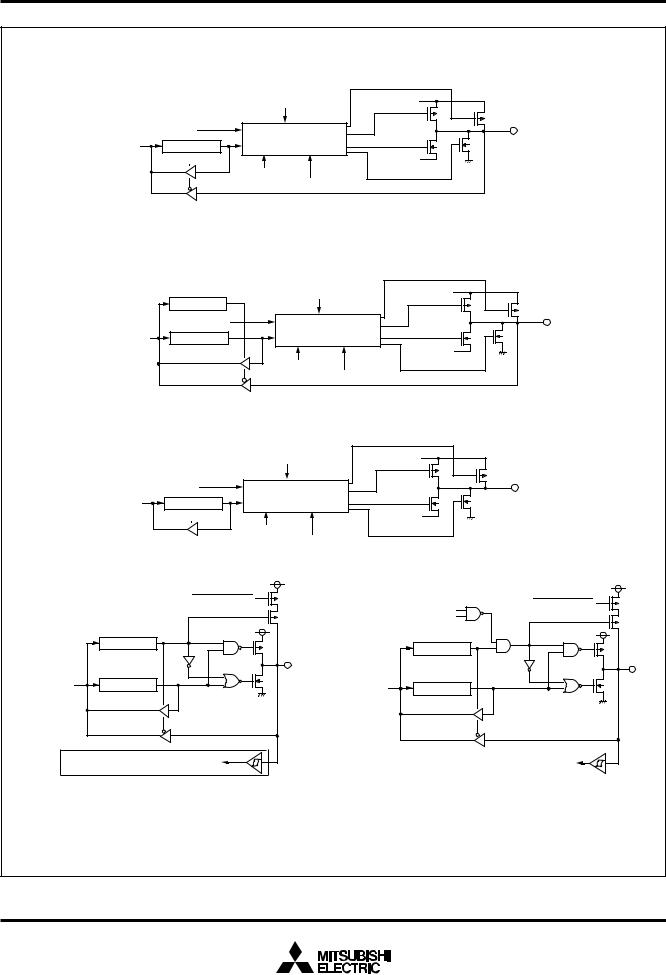
MITSUBISHI MICROCOMPUTERS
3827 Group
SINGLE-CHIP 8-BIT CMOS MICROCOMPUTER
|
(1) Ports P01–P07, P11–P15 |
|
Pull-up |
|
|
||
|
|
|
|
|
|
|
|
|
|
|
LCD drive timing |
|
VL2/VL3/VCC |
|
|
|
|
|
|
Segment/Port |
|
|
|
|
|
|
|
|
|
|
|
|
Segment data |
Interface logic level |
|
|
|
|
|
|
|
|
|
Segment |
|
|
|
|
Data bus |
Port latch |
shift circuit |
|
|
|
|
|
|
|
|
|
|||
|
|
Port direction register |
|
|
VL1/VSS |
|
|
|
|
|
Port/Segment |
|
Port |
|
|
|
|
|
Port direction register |
|
|
||
|
(2) Ports P00, P10 |
|
|
Pull-up |
|
||
|
|
|
|
|
|
||
|
|
|
LCD drive timing |
VL2/VL3/VCC |
|
||
|
|
Direction register |
Segment/Port |
|
|||
|
|
|
|
|
|||
|
|
|
|
|
|
|
|
|
|
Segment data |
Interface logic level |
|
|
||
|
Data bus |
Port latch |
shift circuit |
|
Segment |
|
|
|
|
|
|
|
|||
|
|
|
|
|
|
VL1/VSS |
|
|
|
|
Port/Segment |
|
Port |
|
|
|
|
|
Port direction register |
|
|
||
|
(3) Port P3 |
|
|
|
Pull-up |
|
|
|
|
|
|
|
|
|
|
|
|
|
LCD drive timing |
|
VL2/VL3/VCC |
|
|
|
|
|
|
Segment/Port |
|
|
|
|
|
|
|
|
|
|
|
|
Segment data |
Interface logic level |
|
|
|
|
|
|
|
|
|
Segment |
|
|
|
|
Data bus |
Port latch |
shift circuit |
|
|
|
|
|
|
|
|
|
|||
|
|
|
|
|
VL1/VSS |
|
|
|
|
|
Port/Segment |
|
Port |
|
|
|
|
|
Output control |
|
|
|
|
(4) Ports P16, P17, P2, P41, P42 |
|
(5) Port P44 |
|
|
|||
|
|
Pull-up control |
|
Serial I/O1 enable bit |
Pull-up control |
||
|
|
|
|
|
|||
|
|
|
|
|
|
||
|
|
|
|
|
Reception enable bit |
|
|
|
Direction register |
|
|
|
Direction register |
|
|
|
|
|
|
|
|
||
Data bus |
Port latch |
|
|
Data bus |
Port latch |
|
|
|
|
|
|
|
|||
|
Key input interrupt input |
|
|
|
|
Serial I/O1 input |
|
|
INT1, INT2 interrupt input |
|
|
|
|
||
|
|
|
|
|
|
||
|
Except P16, P17 |
|
|
|
|
|
|
Fig. 10 Port block diagram (1)
14
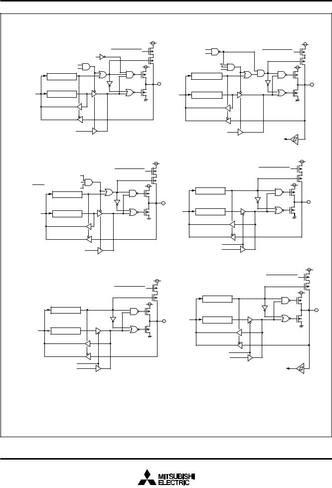
MITSUBISHI MICROCOMPUTERS
3827 Group
SINGLE-CHIP 8-BIT CMOS MICROCOMPUTER
(6) Port P45 |
|
(7) Port P46 |
|
|
|
|
Serial I/O1 clock |
|
|
|
Pull-up control |
selection bit |
Pull-up control |
|
|
Serial I/O1 enable bit |
|||
P45/TxD P-channel output disable bit |
|
|
|
|
Serial I/O1 enable bit |
Serial I/O1 mode selection bit |
|
||
Transmission enable bit |
Serial I/O1 enable bit |
|
||
|
Direction register |
|
Direction register |
|
Data bus |
Port latch |
Data bus |
Port latch |
|
Serial I/O1 output |
Serial I/O1 clock outupt |
|
||
|
|
|
|
Serial I/O1 clock input |
(8) Port P47 |
|
(9) Ports P52, P53 |
Pull-up control |
|
|
Pull-up control |
|
|
|
Serial I/O1 mode selection bit |
|
|
|
|
Serial I/O1 enable bit |
|
|
|
|
SRDY1 output enable bit |
|
Direction register |
|
|
|
Direction register |
|
|
|
|
|
|
|
|
Data bus |
Port latch |
Data bus |
Port latch |
|
|
|
|
||
|
|
Real time control bit |
|
|
Serial I/O1 ready output |
Real time port data |
|
||
(10) Ports P50,P51 |
(11) Port P54 |
Pull-up control |
||
|
|
|
||
|
Pull-up control |
|
|
|
|
|
|
Direction register |
|
|
Direction register |
|
|
|
|
|
Data bus |
Port latch |
|
Data bus |
Port latch |
|
|
|
|
|
|
Pulse output mode |
|
|
|
|
Timer output |
|
PWM function enable bit |
|
|
CNTR0 interrupt input |
|
|
PWM output |
|
|
|
Fig. 11 Port block diagram (2)
15
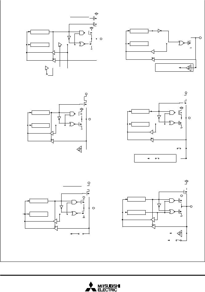
|
MITSUBISHI MICROCOMPUTERS |
|
3827 Group |
|
SINGLE-CHIP 8-BIT CMOS MICROCOMPUTER |
|
|
|
|
(12) Port P43 |
(13) Ports P40, P71–P77 |
|
Pull-up control |
|
Direction register |
Data bus |
Port latch |
TOUT/φ output control Timer output

TOUT/φ selection bit
φ output
|
Direction register |
Data bus |
Port latch |
|
A-D trigger input |
|
Except P71 to P77 |
(14) Port P55
Pull-up control 

|
Direction register |
Data bus |
Port latch |
CNTR1 interrupt input 

(15) Ports P56, P57
Pull-up control 

|
Direction register |
|
Data bus |
Port latch |
|
|
D-A conversion output |
|
|
D-A1, D-A2 output enable bit |
|
Except P57 |
VREF input switch |
|
VREF input selection bit |
||
|
(16) Ports P64–P67
Pull-up control 


|
Direction register |
Data bus |
Port latch |
|
A-D conversion input |
|
Analog input pin selection bit |
(17) Port P60
Pull-up control 


|
Direction register |
Data bus |
Port latch |
|
Serial I/O2 input |
|
A-D conversion input |
|
Analog input pin selection bit |
Fig. 12 Port block diagram (3)
16
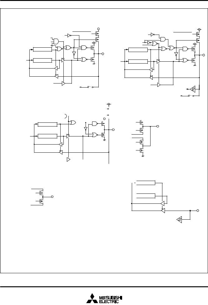
MITSUBISHI MICROCOMPUTERS
3827 Group
SINGLE-CHIP 8-BIT CMOS MICROCOMPUTER
(18) Port P61 |
|
(19) Port P62 |
|
|
|
|
Pull-up control |
Synchronous clock selection bit |
Pull-up control |
|
P61/SOUT2 P-channel output disable bit |
||||
Serial I/O2 transmit completion signal |
Serial I/O2 port selection bit |
|
||
Synchronous clock selection bit |
|
|||
Serial I/O2 port selection bit |
Synchronous clock output pin |
|
||
|
selection bit |
|
||
|
|
|
|
|
|
Direction register |
|
Direction register |
|
Data bus |
Port latch |
Data bus |
Port latch |
|
|
|
|
||
|
Serial I/O2 output |
|
Serial I/O2 clock output |
|
|
A-D conversion input |
|
|
|
|
|
|
Serial I/O2 clock input |
|
|
Analog input pin selection bit |
|
|
|
|
|
|
|
|
|
|
|
|
A-D conversion input |
|
|
|
|
Analog input pin selection bit |
(20) Port P63
|
|
|
|
|
|
|
|
|
|
|
|
|
|
|
|
|
|
|
|
|
|
|
Synchronous clock selection bit |
|
|
|
|
|
|
|
Pull-up control |
|
|
|
|
|
(21) COM0–COM3 |
||||||||
|
|
|
|
|
|
|
|
|
|
|
|
|
|
|
|
|
||||||
Serial I/O2 port selection bit |
|
|
|
|
|
|
|
|
|
|
|
|
|
|
|
|
VL3 |
|
|
|
|
|
|
|
|
|
|
|
|
|
|
|
|
|
|
|
|
|
|
|
|
|
|||
Synchronous clock output pin selection bit |
|
|
|
|
|
|
|
|
|
|
|
|
|
|
|
|
|
|
|
|
|
|
|
|
|
|
|
|
|
|
|
|
|
|
|
|
|
|
|
|
|
|
|
|
|
|
Direction register |
Data bus |
VL2 |
Port latch |
|
|
VL1 |
Serial I/O2 clock output |
|
|
|
VSS |
|
|
A-D conversion input 


Analog input pin selection bit
The gate input signal of each transistor is controlled by the LCD duty ratio and the bias value.
(22) SEG0–SEG17
VL2/VL3
The voltage applied to the sources of
P-channel and N-channel transistors
is the controlled voltage by the bias
value.
VL1/VSS
(23) Port P70
 Direction register
Data bus 
 Port latch
INT0 input
Fig. 13 Port block diagram (4)
17

MITSUBISHI MICROCOMPUTERS
3827 Group
SINGLE-CHIP 8-BIT CMOS MICROCOMPUTER
INTERRUPTS
Interrupts occur by seventeen sources: seven external, nine internal, and one software.
Interrupt Control
Each interrupt except the BRK instruction interrupt have both an interrupt request bit and an interrupt enable bit, and is controlled by the interrupt disable flag. An interrupt occurs if the corresponding interrupt request and enable bits are “1” and the interrupt disable flag is “0.” Interrupt enable bits can be set or cleared by software. Interrupt request bits can be cleared by software, but cannot be set by software. The BRK instruction interrupt and reset cannot be disabled with any flag or bit. The I flag disables all interrupts except the BRK instruction interrupt and reset. If several interrupts requests occurs at the same time the interrupt with highest priority is accepted first.
Table 6 Interrupt vector addresses and priority
Interrupt Operation
Upon acceptance of an interrupt the following operations are auto-
matically performed:
1.The contents of the program counter and processor status register are automatically pushed onto the stack.
2.The interrupt disable flag is set and the corresponding interrupt request bit is cleared.
3.The interrupt jump destination address is read from the vector table into the program counter.
■Notes
When the active edge of an external interrupt (INT0–INT2, CNTR0,
CNTR1) is set or when switching interrupt sources of ADT/A-D
conversion interrupt, the corresponding interrupt request bit may
also be set. Therefore, take following sequence:
(1)Disable the external interrupt which is selected.
(2)Change the active edge in interrupt edge selection register
(timer XY mode register when using CNTR0, CNTR1)
(3)Clear the set interrupt request bit to “0.”
(4)Enable the external interrupt which is selected.
|
Interrupt Source |
Priority |
Vector Addresses (Note 1) |
|
|
|
|
|
|
|
Interrupt Request |
|
|
|
|
|
|
|
|
|
|
|
|
Remarks |
|||||||||||||||||||||||||||||||||||||||||||||||||||||||||||
|
High |
Low |
|
|
|
|
|
Generating Conditions |
|
|
|
|
|
|
|
|
|
|
|
|
|||||||||||||||||||||||||||||||||||||||||||||||||||||||||||||||
|
|
|
|
|
|
|
|
|
|
|
|
|
|
|
|
|
|
|
|
|
|
|
|
|
|
|
|
|
|
|
|
|
|
|
|
|
|
|
|
|
|
|
|
|
|
|
|
|
|
|
|
|
|
|
|||||||||||||||||||||||||||||
|
Reset (Note 2) |
1 |
FFFD16 |
FFFC16 |
|
At reset |
|
Non-maskable |
|||||||||||||||||||||||||||||||||||||||||||||||||||||||||||||||||||||||||||
|
INT0 |
2 |
FFFB16 |
FFFA16 |
|
At detection of either rising or |
|
External interrupt |
|||||||||||||||||||||||||||||||||||||||||||||||||||||||||||||||||||||||||||
|
|
|
|
|
|
|
|
|
|
|
|
|
|
|
|
|
|
|
|
|
falling edge of INT0 input |
|
(active edge selectable) |
||||||||||||||||||||||||||||||||||||||||||||||||||||||||||||
|
INT1 |
3 |
FFF916 |
FFF816 |
|
At detection of either rising or |
|
External interrupt |
|||||||||||||||||||||||||||||||||||||||||||||||||||||||||||||||||||||||||||
|
|
|
|
|
|
|
|
|
|
|
|
|
|
|
|
|
|
|
|
|
falling edge of INT1 input |
|
(active edge selectable) |
||||||||||||||||||||||||||||||||||||||||||||||||||||||||||||
|
|
|
|
|
|
|
|
|
|
|
|
|
|
|
|
|
|
|
|
|
|
|
|
|
|
|
|
|
|
|
|
|
|
|
|
|
|
|
|
|
|
|
|
|
|
|
|
|
|
|
|
|
|
|
|
|
|
|
|
|
|
|
|
|
|
|
|
|
|
|
|
|
|
|
|
|
|
|
|
|
|
|
|
|
Serial I/O1 |
4 |
FFF716 |
FFF616 |
|
At completion of serial I/O1 data |
|
Valid when serial I/O1 is selected |
|||||||||||||||||||||||||||||||||||||||||||||||||||||||||||||||||||||||||||
|
reception |
|
|
|
|
reception |
|
|
|
|
|
|
|
|
|
|
|
|
|
|
|
|
|
|
|
|
|
|
|
|
|
|
|
|
|
|
|
|
|||||||||||||||||||||||||||||||||||||||||||||
|
|
|
|
|
|
|
|
|
|
|
|
|
|
|
|
|
|
|
|
|
|
|
|
|
|
|
|
|
|
|
|
|
|
|
|
|
|
|
|
|
|
|
|
|
|
|
|
|
|
|
|
|
|
|
|
|
|
|
|
|
|
|
|
|
|
|
|
|
|
|
|
|
|
|
|
|
|
|
|
|
|
|
|
|
Serial I/O1 |
5 |
FFF516 |
FFF416 |
|
At completion of serial I/O1 |
|
Valid when serial I/O1 is selected |
|||||||||||||||||||||||||||||||||||||||||||||||||||||||||||||||||||||||||||
|
transmission |
|
|
|
|
transmit shift or when transmis- |
|
|
|
|
|
|
|
|
|
|
|
|
|
|
|
|
|
|
|
|
|
|
|
|
|
|
|
|
|
|
|
|
|||||||||||||||||||||||||||||||||||||||||||||
|
|
|
|
|
|
|
|
|
|
|
|
|
|
|
|
|
|
|
|
|
sion buffer is empty |
|
|
|
|
|
|
|
|
|
|
|
|
|
|
|
|
|
|
|
|
|
|
|
|
|
|
|
|
|
|
|
|
||||||||||||||||||||||||||||||
|
Timer X |
6 |
FFF316 |
FFF216 |
|
At timer X underflow |
|
|
|
|
|
|
|
|
|
|
|
|
|
|
|
|
|
|
|
|
|
|
|
|
|
|
|
|
|
|
|
|
|||||||||||||||||||||||||||||||||||||||||||||
|
|
|
|
|
|
|
|
|
|
|
|
|
|
|
|
|
|
|
|
|
|
|
|
|
|
|
|
|
|
|
|
|
|
|
|
|
|
|
|
|
|
|
|
|
|
|
|
|
|
|
|
|
|
|
|
|
|
|
|
|
|
|
|
|
|
|
|
|
|
|
|
|
|
|
|
|
|
|
|
|
|
|
|
|
Timer Y |
7 |
FFF116 |
FFF016 |
|
At timer Y underflow |
|
|
|
|
|
|
|
|
|
|
|
|
|
|
|
|
|
|
|
|
|
|
|
|
|
|
|
|
|
|
|
|
|||||||||||||||||||||||||||||||||||||||||||||
|
|
|
|
|
|
|
|
|
|
|
|
|
|
|
|
|
|
|
|
|
|
|
|
|
|
|
|
|
|
|
|
|
|
|
|
|
|
|
|
|
|
|
|
|
|
|
|
|
|
|
|
|
|
|
|
|
|
|
|
|
|
|
|
|
|
|
|
|
|
|
|
|
|
|
|
|
|
|
|
|
|
|
|
|
Timer 2 |
8 |
FFEF16 |
FFEE16 |
|
At timer 2 underflow |
|
|
|
|
|
|
|
|
|
|
|
|
|
|
|
|
|
|
|
|
|
|
|
|
|
|
|
|
|
|
|
|
|||||||||||||||||||||||||||||||||||||||||||||
|
|
|
|
|
|
|
|
|
|
|
|
|
|
|
|
|
|
|
|
|
|
|
|
|
|
|
|
|
|
|
|
|
|
|
|
|
|
|
|
|
|
|
|
|
|
|
|
|
|
|
|
|
|
|
|
|
|
|
|
|
|
|
|
|
|
|
|
|
|
|
|
|
|
|
|
|
|
|
|
|
|
|
|
|
Timer 3 |
9 |
FFED16 |
FFEC16 |
|
At timer 3 underflow |
|
|
|
|
|
|
|
|
|
|
|
|
|
|
|
|
|
|
|
|
|
|
|
|
|
|
|
|
|
|
|
|
|||||||||||||||||||||||||||||||||||||||||||||
|
|
|
|
|
|
|
|
|
|
|
|
|
|
|
|
|
|
|
|
|
|
|
|
|
|
|
|
|
|
|
|
|
|
|
|
|
|
|
|
|
|
|
|
|
|
|
|
|
|
|
|
|
|
|
|
|
|
|
|
|
|
|
|
|
|
|
|
|
|
|
|
|
|
|
|
|
|
|
|
|
|
|
|
|
CNTR0 |
10 |
FFEB16 |
FFEA16 |
|
At detection of either rising or |
|
External interrupt |
|||||||||||||||||||||||||||||||||||||||||||||||||||||||||||||||||||||||||||
|
|
|
|
|
|
|
|
|
|
|
|
|
|
|
|
|
|
|
|
|
falling edge of CNTR0 input |
|
(active edge selectable) |
||||||||||||||||||||||||||||||||||||||||||||||||||||||||||||
|
|
|
|
|
|
|
|
|
|
|
|
|
|
|
|
|
|
|
|
|
|
|
|
|
|
|
|
|
|
|
|
|
|
|
|
|
|
|
|
|
|
|
|
|
|
|
|
|
|
|
|
|
|
|
|
|
|
|
|
|
|
|
|
|
|
|
|
|
|
|
|
|
|
|
|
|
|
|
|
|
|
|
|
|
CNTR1 |
11 |
FFE916 |
FFE816 |
|
At detection of either rising or |
|
External interrupt |
|||||||||||||||||||||||||||||||||||||||||||||||||||||||||||||||||||||||||||
|
|
|
|
|
|
|
|
|
|
|
|
|
|
|
|
|
|
|
|
|
falling edge of CNTR1 input |
|
(active edge selectable) |
||||||||||||||||||||||||||||||||||||||||||||||||||||||||||||
|
|
|
|
|
|
|
|
|
|
|
|
|
|
|
|
|
|
|
|
|
|
|
|
|
|
|
|
|
|
|
|
|
|
|
|
|
|
|
|
|
|
|
|
|
|
|
|
|
|
|
|
|
|
|
|
|
|
|
|
|
|
|
|
|
|
|
|
|
|
|
|
|
|
|
|
|
|
|
|
|
|
|
|
|
Timer 1 |
12 |
FFE716 |
FFE616 |
|
At timer 1 underflow |
|
|
|
|
|
|
|
|
|
|
|
|
|
|
|
|
|
|
|
|
|
|
|
|
|
|
|
|
|
|
|
|
|||||||||||||||||||||||||||||||||||||||||||||
|
|
|
|
|
|
|
|
|
|
|
|
|
|
|
|
|
|
|
|
|
|
|
|
|
|
|
|
|
|
|
|
|
|
|
|
|
|
|
|
|
|
|
|
|
|
|
|
|
|
|
|
|
|
|
|
|
|
|
|
|
|
|
|
|
|
|
|
|
|
|
|
|
|
|
|
|
|
|
|
|
|
|
|
|
INT2 |
13 |
FFE516 |
FFE416 |
|
At detection of either rising or |
|
External interrupt |
|||||||||||||||||||||||||||||||||||||||||||||||||||||||||||||||||||||||||||
|
|
|
|
|
|
|
|
|
|
|
|
|
|
|
|
|
|
|
|
|
falling edge of INT2 input |
|
(active edge selectable) |
||||||||||||||||||||||||||||||||||||||||||||||||||||||||||||
|
|
|
|
|
|
|
|
|
|
|
|
|
|
|
|
|
|
|
|
|
|
|
|
|
|
|
|
|
|
|
|
|
|
|
|
|
|
|
|
|
|
|
|
|
|
|
|
|
|
|
|
|
|
|
|
|
|
|
|
|
|
|
|
|
|
|
|
|
|
|
|
|
|
|
|
|
|
|
|
|
|
|
|
|
Serial I/O2 |
14 |
FFE316 |
FFE216 |
|
At completion of serial I/O2 data |
|
Valid when serial I/O2 is selected |
|||||||||||||||||||||||||||||||||||||||||||||||||||||||||||||||||||||||||||
|
|
|
|
|
|
|
|
|
|
|
|
|
|
|
|
|
|
|
|
|
transmission or reception |
|
|
|
|
|
|
|
|
|
|
|
|
|
|
|
|
|
|
|
|
|
|
|
|
|
|
|
|
|
|
|
|
||||||||||||||||||||||||||||||
|
Key input |
15 |
FFE116 |
FFE016 |
|
At falling of conjunction of input |
|
External interrupt |
|||||||||||||||||||||||||||||||||||||||||||||||||||||||||||||||||||||||||||
|
(Key-on wake-up) |
|
|
|
|
level for port P2 (at input mode) |
|
(valid when an “L” level is applied) |
|||||||||||||||||||||||||||||||||||||||||||||||||||||||||||||||||||||||||||
|
|
|
|
|
|
|
|
|
|
|
|
|
|
|
|
|
|
|
|
|
|
|
|
|
|
|
|
|
|
|
|
|
|
|
|
|
|
|
|
|
|
|
|
|
|
|
|
|
|
|
|
|
|
|
|
|
|
|
|
|
|
|
|
|
|
|
|
|
|
|
|
|
|
|
|
|
|
|
|
|
|
|
|
|
ADT |
16 |
FFDF16 |
FFDE16 |
|
At falling of ADT input |
|
Valid when ADT interrupt is se- |
|||||||||||||||||||||||||||||||||||||||||||||||||||||||||||||||||||||||||||
|
|
|
|
|
|
|
|
|
|
|
|
|
|
|
|
|
|
|
|
|
|
|
|
|
|
|
|
|
|
|
|
|
|
|
|
|
|
|
|
|
|
|
|
|
|
|
|
|
|
|
|
|
lected External interrupt |
||||||||||||||||||||||||||||||
|
|
|
|
|
|
|
|
|
|
|
|
|
|
|
|
|
|
|
|
|
|
|
|
|
|
|
|
|
|
|
|
|
|
|
|
|
|
|
|
|
|
|
|
|
|
|
|
|
|
|
|
|
(Valid at falling) |
||||||||||||||||||||||||||||||
|
|
|
|
|
|
|
|
|
|
|
|
|
|
|
|
|
|
|
|
|
|
|
|
|
|
|
|
|
|
|
|
|
|
|
|
|
|
|
|
|
|
|
|
|
|
|
|
|
|
|
|
|
|
|
|
|
|
|
|
|
|
|
|
|
|
|
|
|
|
|
|
|
|
|
|
|
|
|
|
|
|
|
|
|
A-D conversion |
|
|
|
|
At completion of A-D conversion |
|
Valid when A-D interrupt is se- |
|||||||||||||||||||||||||||||||||||||||||||||||||||||||||||||||||||||||||||
|
|
|
|
|
|
|
|
|
|
|
|
|
|
|
|
|
|
|
|
|
|
|
|
|
|
|
|
|
|
|
|
|
|
|
|
|
|
|
|
|
|
|
|
|
|
|
|
|
|
|
|
|
lected |
||||||||||||||||||||||||||||||
|
|
|
|
|
|
|
|
|
|
|
|
|
|
|
|
|
|
|
|
|
|
|
|
|
|
|
|
|
|
|
|
|
|
|
|
|
|
|
|
|
|
|
|
|
|
|
|
|
|
|
|
|
|
|
|
|
|
|
|
|
|
|
|
|
|
|
|
|
|
|
|
|
|
|
|
|
|
|
|
|
|
|
|
|
BRK instruction |
17 |
FFDD16 |
FFDC16 |
|
At BRK instruction execution |
|
Non-maskable software interrupt |
|||||||||||||||||||||||||||||||||||||||||||||||||||||||||||||||||||||||||||
Notes1: Vector addresses contain interrupt jump destination addresses.
2: Reset function in the same way as an interrupt with the highest priority.
18
MITSUBISHI MICROCOMPUTERS
3827 Group
SINGLE-CHIP 8-BIT CMOS MICROCOMPUTER
Interrupt request bit
Interrupt enable bit
Interrupt disable flag (I)
BRK instruction |
Interrupt request |
Reset |
|
Fig. 14 Interrupt control
b7 |
b0 |
Interrupt edge selection register (INTEDGE : address 003A16)
 INT0 interrupt edge selection bit INT1 interrupt edge selection bit INT2 interrupt edge selection bit INT3 interrupt edge selection bit
Not used (return “0” when read)
0 : Falling edge active
1 : Rising edge active
b7 |
|
b0 |
|
|
|
|
|
|
|
b7 |
|
|
|
|
|
|
|
|
b0 |
|
|
|
|
|
|
|
|||||||||||||||||||||||||
Interrupt request register 1 |
|
|
|
Interrupt request register 2 |
|
||||||||||||||||||||||||||||||||||||||||||||||
|
|
|
|
|
|
|
|
|
|
|
|
|
|
|
|
|
|
|
|
|
|
|
|
|
|
|
|
|
|
|
|
|
|
|
|
|
|
|
|
|
|
|
|
||||||||
|
|
|
|
|
|
|
|
|
|
|
|
|
|
|
|
|
|
|
|
|
|
|
|
|
|
|
|
|
|
|
|
|
|
|
|
|
|
|
|
|
|
|
|
(IREQ2 : address 003D16) |
|
||||||
|
|
|
|
|
|
|
|
|
|
|
|
|
|
|
|
|
(IREQ1 : address 003C16) |
|
|
|
|
|
|
|
|
|
|
|
|
|
|
|
|
||||||||||||||||||
|
|
|
|
|
|
|
|
|
|
|
|
|
|
|
|
|
|
|
|
|
|
|
|
|
|
|
|
|
|
|
|
|
|
|
|
|
|
|
|
|
|
|
|
|
|
|
|
|
|
|
|
|
|
|
|
|
|
|
|
|
|
|
|
|
|
|
|
|
|
|
|
INT0 interrupt request bit |
|
|
|
|
|
|
|
|
|
|
|
|
|
|
|
|
|
|
|
|
|
|
|
CNTR0 interrupt request bit |
|
||||||
|
|
|
|
|
|
|
|
|
|
|
|
|
|
|
|
|
|
|
|
|
|
|
|
|
|
|
|
|
|
|
|
|
|
|
|
|
|
|
|
|
|
|
|
||||||||
|
|
|
|
|
|
|
|
|
|
|
|
|
|
|
|
|
|
|
|
|
|
|
|
|
|
|
|
|
|
|
|
|
|
|
|
|
|
|
|
|
|
|
|
||||||||
|
|
|
|
|
|
|
|
|
|
|
|
|
|
|
|
|
|
|
|
INT1 interrupt request bit |
|
|
|
|
|
|
|
|
|
|
|
|
|
|
|
|
|
|
|
|
|
|
|
CNTR1 interrupt request bit |
|
||||||
|
|
|
|
|
|
|
|
|
|
|
|
|
|
|
|
|
|
|
|
|
|
|
|
|
|
|
|
|
|
|
|
|
|
|
|
|
|
|
|
|
|
|
|
||||||||
|
|
|
|
|
|
|
|
|
|
|
|
|
|
|
|
|
|
|
|
|
|
|
|
|
|
|
|
|
|
|
|
|
|
|
|
|
|
|
|
|
|
|
|
||||||||
|
|
|
|
|
|
|
|
|
|
|
|
|
|
|
|
|
|
|
|
Serial I/O1 receive interrupt request bit |
|
|
|
|
|
|
|
|
|
|
|
|
|
|
|
|
|
|
|
|
|
|
|
Timer 1 interrupt request bit |
|
||||||
|
|
|
|
|
|
|
|
|
|
|
|
|
|
|
|
|
|
|
|
|
|
|
|
|
|
|
|
|
|
|
|
|
|
|
|
|
|
|
|
|
|
|
|
||||||||
|
|
|
|
|
|
|
|
|
|
|
|
|
|
|
|
|
|
|
|
Serial I/O1 transmit interrupt request bit |
|
|
|
|
|
|
|
|
|
|
|
|
|
|
|
|
|
|
|
|
|
|
|
INT2 interrupt request bit |
|
||||||
|
|
|
|
|
|
|
|
|
|
|
|
|
|
|
|
|
|
|
|
|
|
|
|
|
|
|
|
|
|
|
|
|
|
|
|
|
|
|
|
|
|
|
|
||||||||
|
|
|
|
|
|
|
|
|
|
|
|
|
|
|
|
|
|
|
|
|
|
|
|
|
|
|
|
|
|
|
|
|
|
|
|
|
|
|
|
|
|
|
|
||||||||
|
|
|
|
|
|
|
|
|
|
|
|
|
|
|
|
|
|
|
|
Timer X interrupt request bit |
|
|
|
|
|
|
|
|
|
|
|
|
|
|
|
|
|
|
|
|
|
|
|
Serial I/O2 interrupt request bit |
|
||||||
|
|
|
|
|
|
|
|
|
|
|
|
|
|
|
|
|
|
|
|
|
|
|
|
|
|
|
|
|
|
|
|
|
|
|
|
|
|
|
|
|
|
|
|
||||||||
|
|
|
|
|
|
|
|
|
|
|
|
|
|
|
|
|
|
|
|
|
|
|
|
|
|
|
|
|
|
|
|
|
|
|
|
|
|
|
|
|
|
|
|
||||||||
|
|
|
|
|
|
|
|
|
|
|
|
|
|
|
|
|
|
|
|
Timer Y interrupt request bit |
|
|
|
|
|
|
|
|
|
|
|
|
|
|
|
|
|
|
|
|
|
|
|
Key input interrupt request bit |
|
||||||
|
|
|
|
|
|
|
|
|
|
|
|
|
|
|
|
|
|
|
|
|
|
|
|
|
|
|
|
|
|
|
|
|
|
|
|
|
|
|
|
|
|
|
|
||||||||
|
|
|
|
|
|
|
|
|
|
|
|
|
|
|
|
|
|
|
|
|
|
|
|
|
|
|
|
|
|
|
|
|
|
|
|
|
|
|
|
|
|
|
|
||||||||
|
|
|
|
|
|
|
|
|
|
|
|
|
|
|
|
|
|
|
|
Timer 2 interrupt request bit |
|
|
|
|
|
|
|
|
|
|
|
|
|
|
|
|
|
|
|
|
|
|
|
ADT/AD conversion interrupt request bit |
|
||||||
|
|
|
|
|
|
|
|
|
|
|
|
|
|
|
|
|
|
|
|
|
|
|
|
|
|
|
|
|
|
|
|
|
|
|
|
|
|
|
|
|
|
|
|
||||||||
|
|
|
|
|
|
|
|
|
|
|
|
|
|
|
|
|
|
|
|
|
|
|
|
|
|
|
|
|
|
|
|
|
|
|
|
|
|
|
|
|
|
|
|
||||||||
|
|
|
|
|
|
|
|
|
|
|
|
|
|
|
|
|
|
|
|
Timer 3 interrupt request bit |
|
|
|
|
|
|
|
|
|
|
|
|
|
|
|
|
|
|
|
|
|
|
|
Not used (returns “0” when read) |
|
||||||
|
|
|
|
|
|
|
|
|
|
|
|
|
|
|
|
|
|
|
|
|
|
|
|
|
|
|
|
|
|
|
|
|
|
|
|
|
|
|
|
|
|
|
|
||||||||
|
|
|
|
|
|
|
|
|
|
|
|
|
|
|
|
|
|
|
|
|
|
|
|
|
|
|
|
|
|
|
|
|
|
|
|
|
|
|
|
|
|
|
|
||||||||
|
|
|
|
|
|
|
|
|
|
|
|
|
|
|
|
|
|
|
|
|
|
|
|
|
|
|
|
|
|
|
|
|
|
|
|
|
|
|
|
|
|
|
|
|
|
|
|
|
|
|
|
|
|
|
|
|
|
|
|
|
|
|
|
|
|
|
|
|
|
|
|
|
|
|
|
|
|
|
|
|
|
|
|
|
|
|
|
|
|
|
|
|
|
|
|
|
|
|
|
|
|
|
|
|
|
|
|
|
|
|
|
|
|
|
|
|
|
|
|
|
|
|
|
|
|
|
|
|
|
|
|
|
|
|
|
|
|
|
|
|
|
|
|
0 : No interrupt request issued |
|
|
|||||||||
|
|
|
|
|
|
|
|
|
|
|
|
|
|
|
|
|
|
|
|
|
|
|
|
|
|
|
|
|
|
|
|
|
|
|
|
|
|
|
|
1 : Interrupt request issued |
|
|
|||||||||
|
|
|
|
|
|
|
|
|
|
|
|
|
|
|
|
|
|
|
|
|
|
|
|
|
|
|
|
|
|
|
|
||||||||||||||||||||
b7 |
|
b0 |
|
|
|
|
|
|
|
b7 |
|
|
|
|
|
|
|
b0 |
|
|
|
|
|
|
|
||||||||||||||||||||||||||
Interrupt control register 1 |
Interrupt control register 2 |
|
|||||||||||||||||||||||||||||||||||||||||||||||||
|
|
|
|
|
|
|
|
|
|
|
|
|
|
|
|
|
|
|
|
|
|
|
|
|
|
|
|
|
|
|
|
|
|
|
|
|
|
|
|
|
|
|
|
||||||||
|
|
|
|
|
|
|
|
|
|
|
|
|
|
|
|
(ICON1 : address 003E16) |
|
|
|
|
|
|
|
|
|
|
|
|
|
|
|
|
|
|
|
(ICON2 : address 003F16) |
|
||||||||||||||
|
|
|
|
|
|
|
|
|
|
|
|
|
|
|
|
|
|
|
|
|
|
|
|
|
|
|
|
|
|
|
|
|
|
|
|
|
|
|
|
|
|
|
|
|
|
|
|
|
|||
|
|
|
|
|
|
|
|
|
|
|
|
|
|
|
|
|
|
|
|
INT0 interrupt enable bit |
|
|
|
|
|
|
|
|
|
|
|
|
|
|
|
|
|
|
|
|
|
|
|
|
CNTR0 interrupt enable bit |
|
|||||
|
|
|
|
|
|
|
|
|
|
|
|
|
|
|
|
|
|
|
|
|
|
|
|
|
|
|
|
|
|
|
|
|
|
|
|
|
|
|
|
|
|
|
|
|
|||||||
|
|
|
|
|
|
|
|
|
|
|
|
|
|
|
|
|
|
|
|
INT1 interrupt enable bit |
|
|
|
|
|
|
|
|
|
|
|
|
|
|
|
|
|
|
|
|
|
|
|
|
CNTR1 interrupt enable bit |
|
|||||
|
|
|
|
|
|
|
|
|
|
|
|
|
|
|
|
|
|
|
|
|
|
|
|
|
|
|
|
|
|
|
|
|
|
|
|
|
|
|
|
|
|
|
|
|
|||||||
|
|
|
|
|
|
|
|
|
|
|
|
|
|
|
|
|
|
|
|
Serial I/O receive interrupt enable bit |
|
|
|
|
|
|
|
|
|
|
|
|
|
|
|
|
|
|
|
|
|
|
|
|
Timer 1 interrupt enable bit |
|
|||||
|
|
|
|
|
|
|
|
|
|
|
|
|
|
|
|
|
|
|
|
|
|
|
|
|
|
|
|
|
|
|
|
|
|
|
|
|
|
|
|
|
|
|
|
|
|||||||
|
|
|
|
|
|
|
|
|
|
|
|
|
|
|
|
|
|
|
|
Serial I/O transmit interrupt enable bit |
|
|
|
|
|
|
|
|
|
|
|
|
|
|
|
|
|
|
|
|
|
|
|
|
INT2 interrupt enable bit |
|
|||||
|
|
|
|
|
|
|
|
|
|
|
|
|
|
|
|
|
|
|
|
|
|
|
|
|
|
|
|
|
|
|
|
|
|
|
|
|
|
|
|
|
|
|
|
|
|||||||
|
|
|
|
|
|
|
|
|
|
|
|
|
|
|
|
|
|
|
|
Timer X interrupt enable bit |
|
|
|
|
|
|
|
|
|
|
|
|
|
|
|
|
|
|
|
|
|
|
|
|
Serial I/O2 interrupt enable bit |
|
|||||
|
|
|
|
|
|
|
|
|
|
|
|
|
|
|
|
|
|
|
|
|
|
|
|
|
|
|
|
|
|
|
|
|
|
|
|
|
|
|
|
|
|
|
|
|
|||||||
|
|
|
|
|
|
|
|
|
|
|
|
|
|
|
|
|
|
|
|
Timer Y interrupt enable bit |
|
|
|
|
|
|
|
|
|
|
|
|
|
|
|
|
|
|
|
|
|
|
|
|
Key input interrupt enable bit |
|
|||||
|
|
|
|
|
|
|
|
|
|
|
|
|
|
|
|
|
|
|
|
|
|
|
|
|
|
|
|
|
|
|
|
|
|
|
|
|
|
|
|
|
|
|
|
|
|||||||
|
|
|
|
|
|
|
|
|
|
|
|
|
|
|
|
|
|
|
|
Timer 2 interrupt enable bit |
|
|
|
|
|
|
|
|
|
|
|
|
|
|
|
|
|
|
|
|
|
|
|
|
ADT/AD conversion interrupt enable bit |
|
|||||
|
|
|
|
|
|
|
|
|
|
|
|
|
|
|
|
|
|
|
|
|
|
|
|
|
|
|
|
|
|
|
|
|
|
|
|
|
|
|
|
|
|
|
|
|
|||||||
|
|
|
|
|
|
|
|
|
|
|
|
|
|
|
|
|
|
|
|
Timer 3 interrupt enable bit |
|
|
|
|
|
|
|
|
|
|
|
|
|
|
|
|
|
|
|
|
|
|
|
|
Not used (returns “0” when read) |
|
|||||
|
|
|
|
|
|
|
|
|
|
|
|
|
|
|
|
|
|
|
|
|
|
|
|
|
|
|
|
|
|
|
|
|
|
|
|
|
|
|
|
|
|
|
|
|
|||||||
|
|
|
|
|
|
|
|
|
|
|
|
|
|
|
|
|
|
|
|
|
|
|
|
|
|
|
|
|
|
|
|
|
|
|
|
|
|
|
|
|
|
|
|
|
|
|
(Do not write “1” to this bit.) |
|
|||
|
|
|
|
|
|
|
|
|
|
|
|
|
|
|
|
|
|
|
|
|
|
|
|
|
|
|
|
|
|
|
|
|
|
|
|
|
|
|
|
|
|
|
|
|
|
|
|
|
|
|
|
0 : Interrupts disabled
1 : Interrupts enabled
Fig. 15 Structure of interrupt-related registers
19
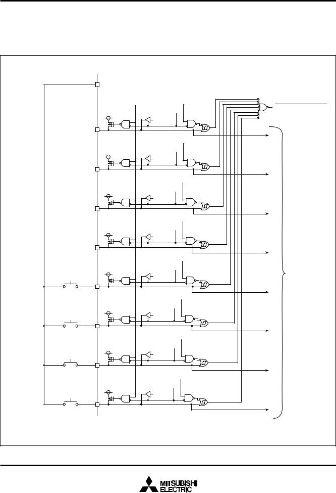
MITSUBISHI MICROCOMPUTERS
3827 Group
SINGLE-CHIP 8-BIT CMOS MICROCOMPUTER
Key Input Interrupt (Key-on wake-up)
A Key-on wake up interrupt request is generated by applying “L” level to any pin of port P2 that have been set to input mode. In other words, it is generated when AND of input level goes from “1”
to “0”. An example of using a key input interrupt is shown in Figure
16, where an interrupt request is generated by pressing one of the keys consisted as an active-low key matrix which inputs to ports P20–P23.
Port PXx |
|
|
|
|
“L” level output |
|
|
||
|
PULLA register |
Key input control register = “1” |
|
|
|
Bit 2 = “1” |
|
||
|
Port P27 |
Key input interrupt request |
||
|
direction register = “1” |
|
||
|
|
Port P27 |
|
|
Port P27 output |
|
latch |
|
|
|
|
|
||
|
|
Key input control register = “1” |
|
|
|
Port P26 |
|
||
|
direction register = “1” |
|
||
|
|
Port P26 |
|
|
|
|
|
||
Port P26 output |
|
latch |
|
|
|
|
|
||
|
|
Key input control register = “1” |
|
|
|
Port P25 |
|
||
|
direction register = “1” |
|
||
|
|
Port P25 |
|
|
|
|
|
||
Port P25 output |
|
latch |
|
|
|
|
|
||
|
|
Key input control register = “1” |
|
|
|
Port P24 |
|
||
|
direction register = “1” |
|
||
|
|
Port P24 |
|
|
Port P24 output |
|
latch |
|
|
|
|
|
||
|
|
Key input control register = “1” |
|
|
|
Port P23 |
|
||
|
direction register = “0” |
Port P2 input |
||
|
Port P23 |
|||
reading circuit |
||||
Port P23 |
|
latch |
||
|
|
|||
input |
|
|
|
|
|
|
Key input control register = “1” |
|
|
|
Port P22 |
|
||
|
direction register = “0” |
|
||
|
|
Port P22 |
|
|
Port P22 |
|
latch |
|
|
input |
|
|
|
|
|
|
Key input control register = “1” |
|
|
|
Port P21 |
|
||
|
direction register = “0” |
|
||
|
|
Port P21 |
|
|
Port P21 |
|
latch |
|
|
input |
|
|
|
|
|
|
Key input control register = “1” |
|
|
|
Port P20 |
|
||
|
direction register = “0” |
|
||
|
Port P20 |
|
||
Port P20 |
|
latch |
|
|
input |
|
|
|
|
|
|
|
P-channel transistor for pull-up |
|
|
|
|
CMOS output buffer |
|
Fig. 16 Connection example when using key input interrupt and port P2 block diagram |
|
|||
20 |
|
|
|
|
MITSUBISHI MICROCOMPUTERS
3827 Group
SINGLE-CHIP 8-BIT CMOS MICROCOMPUTER
TIMERS
The 3827 group has five timers: timer X, timer Y, timer 1, timer 2, and timer 3. Timer X and timer Y are 16-bit timers, and timer 1, timer 2, and timer 3 are 8-bit timers.
All timers are down count timers. When the timer reaches “0016”, an underflow occurs at the next count pulse and the corresponding timer latch is reloaded into the timer and the count is continued. When a timer underflows, the interrupt request bit cor-
responding to that timer is set to “1”.
Read and write operation on 16-bit timer must be performed for both high and low-order bytes. When reading a 16-bit timer, read the high-order byte first. When writing to a 16-bit timer, write the low-order byte first. The 16-bit timer cannot perform the correct operation when reading during the write operation, or when writing during the read operation.
Real time port |
|
|
|
|
Data bus |
|
|||
control bit |
“1” |
|
|
|
|
|
|||
Q D |
|
|
|
|
|
||||
P52 |
|
|
P52 data for real time port |
|
|
||||
|
|
|
|
|
|
|
|
||
P52 direction register |
|
“0” |
Latch |
|
|
|
|
|
|
P52 latch |
|
|
|
|
|
||||
|
|
|
|
|
|
||||
Real time port |
|
|
|
|
|
|
|||
control bit |
“1” |
Q D |
P53 data for real time port |
|
|
||||
P53 |
|
|
|
|
|||||
|
|
|
|
|
|
|
|
||
P53 direction register |
|
“0” |
Latch |
Real time port |
|
|
|
||
P53 latch |
control bit |
“0” |
Timer X mode register |
|
|||||
|
|
|
|
||||||
f(XIN)/16 |
|
|
|
|
“1” |
write signal |
|
|
|
|
|
|
|
|
|
|
|
||
(f(XIN)/16 in low-speed mode ) |
Timer X stop |
|
Timer X write |
|
|||||
|
|
|
|
control bit |
|
|
|||
CNTR0 active |
Timer X operat- |
|
control bit |
|
|||||
|
|
|
|
||||||
edge switch bit |
ing mode bits |
|
Timer X (low) latch (8) |
Timer X (high) latch (8) |
|
||||
“00”,“01”,“11” |
Timer X |
||||||||
|
“0” |
||||||||
|
|
|
|
|
|
||||
P54/CNTR0 |
|
|
Timer X (low) (8) |
Timer X (high) (8) |
interrupt |
||||
|
|
|
|
||||||
|
|
|
“10” |
|
|
|
|
request |
|
|
“1” |
|
|
|
|
|
|||
|
|
|
|
|
|
|
|||
Pulse width |
|
|
|
|
|
|
CNTR0 |
||
measurement |
|
|
|
|
|
interrupt |
|||
mode |
CNTR0 active |
|
Pulse output mode |
|
request |
||||
|
edge switch bit “0” |
Q S |
|
|
|
|
|||
|
|
|
|
|
|
|
|
||
|
|
|
“1” |
T |
|
|
Timer Y operating mode bit |
|
|
P54 direction register |
|
|
Q |
|
|
“00”,“01”,“10” |
CNTR1 |
||
|
|
|
|
|
|||||
|
|
|
|
|
Pulse width HL continuously measurement mode |
interrupt |
|||
|
|
|
P54 latch |
|
|
||||
|
|
|
|
|
|
|
request |
||
|
|
|
|
|
|
|
|
||
Pulse output mode |
|
Rising edge detection |
“11” |
|
|||||
|
|
|
Period |
|
|||||
|
|
|
|
|
Falling edge detection |
measurement mode |
|
||
|
|
|
|
|
|
|
|||
|
f(XIN)/16 |
|
|
|
|
|
|
|
(f(XCIN) 16 in φ = XCIN divided by 2) |
|
|
|
|||
|
|
|
Timer Y stop |
|
|
|
|
CNTR1 active |
|
|
control bit |
|
|
|
|
|
|
|
|
|
|
|
|
edge switch bit |
“00”,“01”,“11” |
Timer Y (low) latch (8) |
Timer Y (high) latch (8) |
Timer Y |
|||
“0” |
|
|
|
|
|
|
|
P55/CNTR1 |
|
|
|
Timer Y (low) (8) |
Timer Y (high) (8) |
|
interrupt |
|
“10”Timer Y operating |
|
|
|
request |
||
“1” |
|
|
|
|
|||
|
mode bit |
|
|
|
|
|
|
|
|
|
|
|
|
|
|
f(XIN)/16 |
|
|
|
|
|
|
Timer 1 |
(f(XCIN)/16 in φ = XCIN divided by 2) |
|
|
|
|
|||
|
|
|
|
interrupt |
|||
Timer 1 count source |
|
Timer 2 count source |
Timer 2 write |
request |
|||
selection bit |
|
Timer 1 latch (8) |
selection bit |
Timer 2 latch (8) |
control bit |
|
|
“0” |
“0” |
|
Timer 2 |
||||
|
|
|
|
|
|
||
|
|
Timer 1 (8) |
|
|
|
||
XCIN |
|
|
Timer 2 (8) |
|
interrupt |
||
“1” |
|
|
“1” |
|
|
request |
|
|
|
|
|
|
|
|
|
|
|
|
|
f(XIN)/16 |
|
|
|
|
|
|
|
(f(XCIN) 16 in φ=XCIN divided by 2) |
|
|
|
|
|
|
|
|
|
|
|
|
|
TOUT output |
|
|
|
|
|
|
|
|
|
|
|
|
|
|
|
|
|
||||||
|
|
|
|
|
|
|
|
|
|
TOUT output |
|
|
|
|
|
|
|
|
|
|
|
|
|
|
|
||||||||
|
|
|
TOUT output |
active edge |
control bit |
|
|
|
|
|
|
|
|
|
|
|
|
|
|
|
|||||||||||||
|
|
|
switch bit |
|
|
|
|
|
|
|
|
|
|
|
|
|
|
|
|
|
|
|
|
||||||||||
|
|
|
control bit |
|
“0” |
|
|
|
|
|
|
|
|
|
|
|
|
|
|
|
|
|
|
|
|
||||||||
P43/φ/TOUT |
|
|
|
|
|
Q S |
|
|
|
|
|
|
|
|
|
|
|
|
|
|
|
|
|||||||||||
|
|
|
|
|
|
|
|
|
|
|
|
|
|
|
|
|
|
|
|
|
|
|
|
|
|
|
|
|
|
|
|||
|
|
|
|
|
|
|
|
|
|
|
|
|
|
|
|
T |
|
|
|
|
|
|
|
|
|
|
|
|
|
|
|
|
|
|
|
|
|
|
|
|
|
|
|
|
“1” |
|
|
|
|
|
|
|
|
|
|
|
|
|
|
|
|
|
|
|
|
|
|
|
|
|
|
|
|
|
|
|
|
|
|
|
|
|
|
|
|
|
|
|
|
|
|
|
|
|
|
|
|
|
|||
P43 direction |
register |
|
|
|
P43 latch |
|
|
|
Q |
|
|
“0” |
|
Timer 3 latch (8) |
|
|
|
|
|
|
Timer 3 |
||||||||||||
|
|
|
|
|
|
|
|
|
|
|
|
|
|
|
|||||||||||||||||||
|
|
|
|
|
|
|
|
|
|
|
|
|
|
|
|
||||||||||||||||||
|
|
|
|
|
|
|
|
|
|
|
|
|
|
|
|
|
|
|
|
|
|
|
|
|
|
|
|
|
|
|
|
|
|
|
|
|
|
|
|
|
|
|
|
|
|
|
|
|
|
|
|
|
|
|
|
|
|
|
|
|
|
|
|
|
|
|
|
|
f(XIN)/16(f(XCIN)/16 in low-speed mode ) |
|
|
|
|
|
Timer 3 (8) |
|
|
|
|
|
|
interrupt |
|||||||||||||||||||
|
|
|
|
|
|
|
|
|
|
|
|||||||||||||||||||||||
|
|
“1” |
|
|
|
|
|
|
|
|
|
|
request |
||||||||||||||||||||
|
|
|
|
|
|
|
|
|
|
|
|
|
|
|
|
|
|
|
|
|
|
|
|
|
|
|
|
|
|
||||
|
|
|
|
|
|
|
|
|
|
|
|
|
|
|
|
|
|
|
|
|
|
|
|
|
|
|
|
|
|
|
|||
|
|
|
|
|
|
|
|
|
|
|
|
|
|
|
|
|
|
|
Timer 3 count |
|
|
|
|
|
|
|
|
|
|||||
|
|
|
|
|
|
|
|
|
|
|
|
|
|
|
|
|
|
|
source selection bit |
|
|
|
|
|
|
|
|
|
|||||
|
|
|
|
|
|
|
|
|
|
|
|
|
|
|
|
|
|
|
|
|
|
|
|
|
|
|
|
|
|
|
|
|
|
Fig. 17 Timer block diagram
21
Loading...