


GR-D20
SERVICE MANUAL
COPYRIGHT © 2003 VICTOR COMPANY OF JAPAN, LTD.
No.86730
2003/04
DIGITAL VIDEO CAMERA
86730200304
GR-D20EK,GR-D20E
X
,GR-D20E
Y
,GR-D20E
Z
,GR-D21EK,
GR-D40EK,GR-D40E
X
,GR-D40E
Y
,GR-D40E
Z
SPECIFICATION
Camcorder
General
Digital Video Camera
Connectors
AC Adapter
For disassembling and assembling of MECHANISM ASSEMBLY, refer to the SERVICE MANUAL No.86700 (MECHANISM ASSEMBLY).
PAL
Power supply : DC 11.0 V (Using AC Adapter)
DC 7.2 V (Using battery pack)
Power consumption
LCD monitor off, viewfinder on : Approx. 3.4 W
LCD monitor on, viewfinder off : Approx. 4.7 W
Dimensions (W x H x D) : 69 mm x 94 mm x 143 mm
(with the LCD monitor closed and the viewfinder pushed
back in)
Weight : Approx. 525 g
Operating temperature : 0°C to 40°C
Operating humidity : 35% to 80%
Storage temperature : -20°C to 50°C
Pickup : 1/6" CCD
Lens : F 1.6, f = 2.7 mm to 43.2 mm, 16:1 power zoom lens
Filter diameter : Ø37 mm
LCD monitor : 2.5" diagonally measured, LCD panel/TFT active
matrix system
Viewfinder : Electronic viewfinder with 0.24" black/white LCD
Speaker : Monaural
Format : DV format (SD mode)
Signal format : PAL standard
Recording/Playback format : Video: Digital component recording
: Audio: PCM digital recording,
32 kHz 4-channel (12-bit),
48 kHz 2-channel (16-bit)
Cassette : Mini DV cassette
Tape speed : SP : 18.8 mm/s
LP : 12.5 mm/s
Maximum recording time : SP : 80 min.
(using 80 min. cassette) LP : 120 min.
S-Video
Output : Y : 1 V (p-p), 75 Ω, analogue
C : 0.29 V (p-p), 75 Ω, analogue
Input* : Y : 0.8 V (p-p) -1.2 V (p-p), 75 Ω, analogue
C : 0.2 V (p-p) -0.4 V (p-p), 75 Ω, analogue
AV
Video output : 1 V (p-p), 75 Ω, analogue
Video input* : 0.8 V (p-p) -1.2 V (p-p), 75 Ω, analogue
Audio output : 300 mV (rms), 1 kΩ, analogue, stereo
Audio input* : 300 mV (rms), 50 kΩ, analogue, stereo
DV
Output : 4-pin, IEEE 1394 compliant
Input* : 4-pin, IEEE 1394 compliant
USB** :5-pin
EDIT Ø3.5 mm, 2-pole
* GR-D50/D30 only
** GR-D50/D40 only
Power requirement AC 110 V to 240 V ~, 50 Hz/60 Hz
Output : DC 11 V , 1 A
Specifications shown are for SP mode unless otherwise indicated. E & O.E. Design and specifications subject
to change without notice.
GR-D20EK,GR-D20EX,GR-D20EY,GR-D20EZ,GR-D21EK,GR-D40EK,GR-D40EX,GR-D40EY,GR-D40EZ M3D122,M3D124
1-6 (No.86730)
1.Torque driver
Be sure to use to fastening the mechanism and exterior parts
because those parts must strictly be controlled for tightening
torque.
2.Bit
This bit is slightly longer than those set in conventional torque
drivers.
3.Tweezers
To be used for removing and installing parts and wires.
4.Chip IC replacement jig
To be used for replacement of IC.
5.Cleaning cloth
Recommended cleaning cloth to wipe down the video heads,
mechanism (tape transport system), optical lens surface.
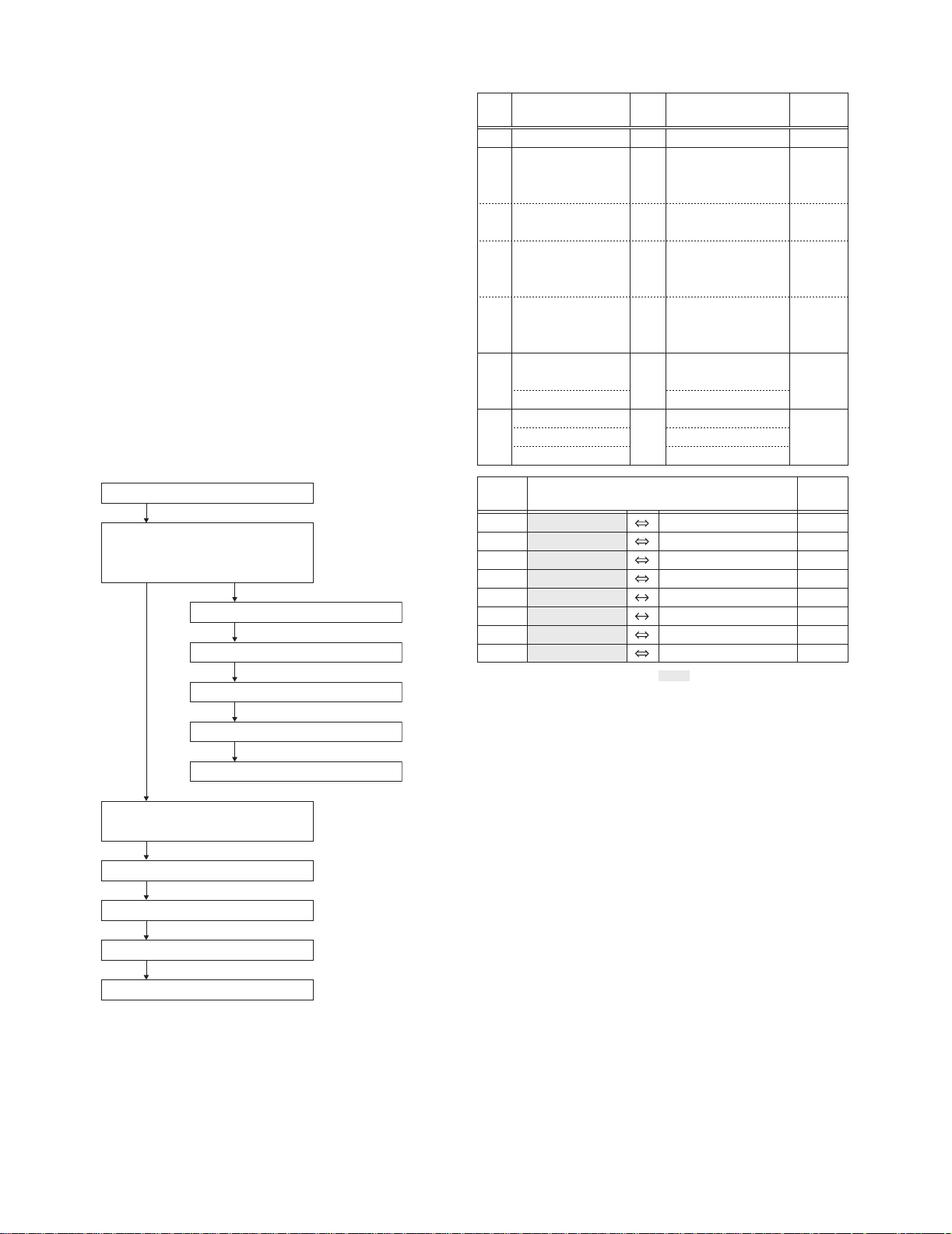
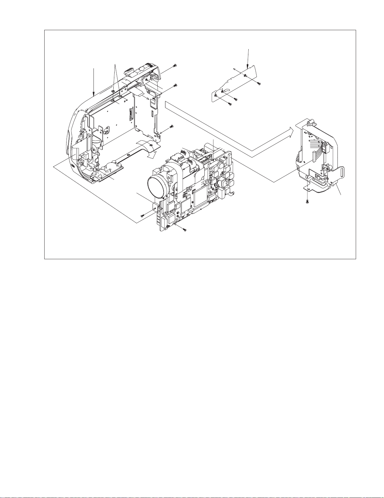
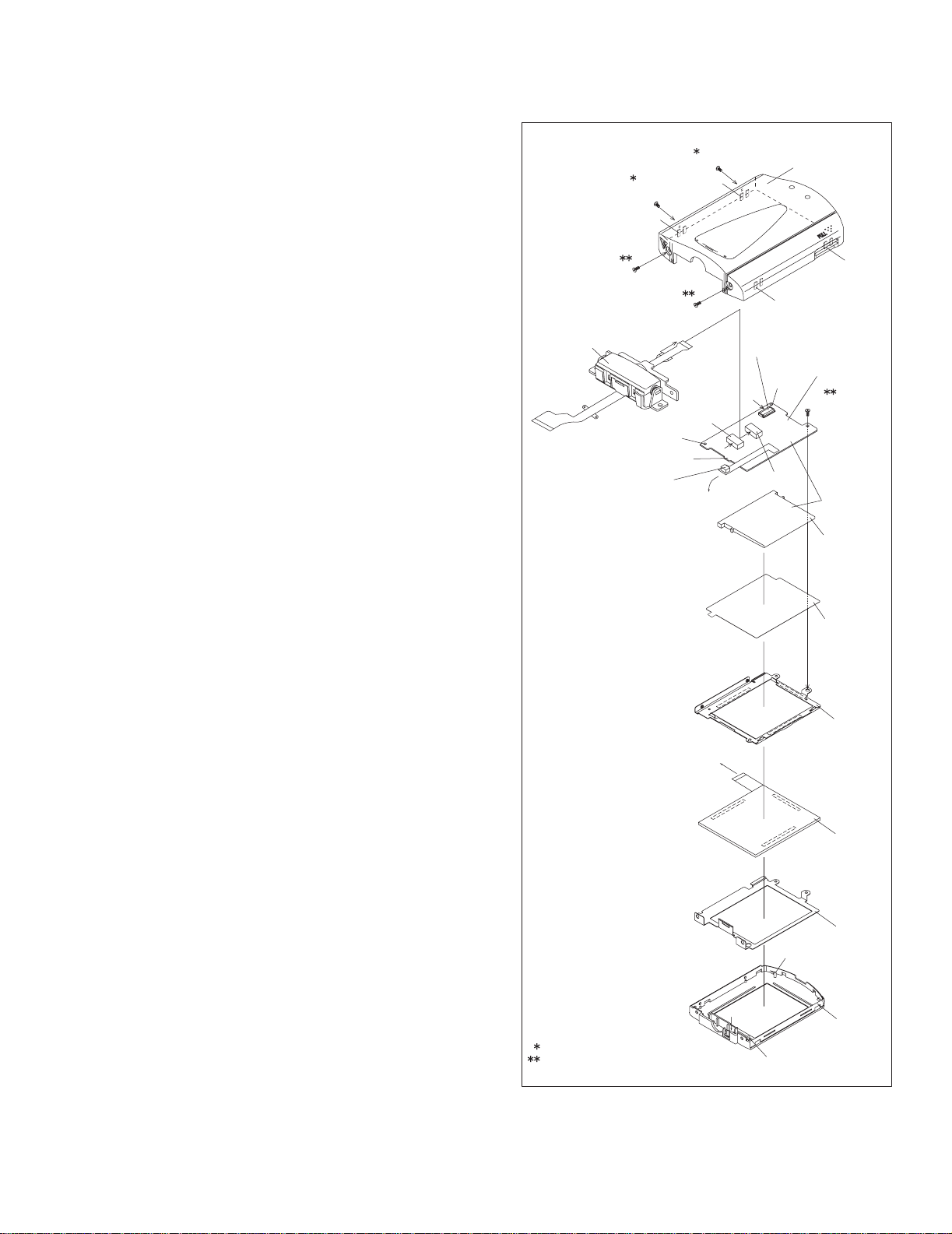
2.2 ASSEMBLY AND DISASSEMBLY OF CABINET PARTS
2.2.1 Disassembly flow chart
This flowchart indicates the disassembly step for the cabinet
parts and board assembly in order to gain access to item(s) to be
serviced. When reassembling, perform the step(s) in reverse or-
der.
2.2.2 Disassembly method
NOTE 8a:
Take care not to cut the FPC wire when and after removing the
VF ASSEMBLY.
NOTE 8b:
As for disassembly/assembly of [8]VF ASSEMBLY, see 2.4
ASSEMBLY AND DISASSEMBLY OF [8] VF ASSEMBLY.
NOTE 10a:
Take care not to cut the FPC when and after removing the
MONITOR ASSEMBLY.
NOTE 10b:
As for disassembly/assembly of [10] MONITOR ASSEMBLY,
see 2.5 ASSEMBLY AND DISASSEMBLY OF [10] MONITOR
ASSEMBLY.
NOTE 11a:
Before removing the MONI-BW BOARD ASSEMBLY, check
whether MEMORY CARD is inserted or not. If MEMORY
CARD is inserted, pull out the MEMORY CARD before remov-
ing the MONI-BW BOARD ASSEMBLY.
NOTE 11b:
Since the SPEAKER is soldered to the MONI-BW BOARD AS-
SEMBLY, the SPEAKER should not be separated from the
MONI-BW BOARD ASSEMBLY except when replacing the
SPEAKER.
NOTE 11c:
Take care not to lose the KNOB(SLIDE). When attaching the
KNOB(SLIDE), attach the KNOB(SLIDE) in a proper position.
NOTE 3:
After removing the FRONT COVER ASSEMBLY, OP BLOCK
ASSEMBLY is not covered with anything. Take care not to
damage the OP BLOCK ASSEMBLY when and after removing
the FRONT COVER ASSEMBLY.
[1]
[2]
TOP COVER ASSEMBLY
UPPER ASSEMBLY
(Inc. VF ASSEMBLY,
SPEAKER/MONITOR)
[8]
VF ASSEMBLY
[9]
COVER(UPPER)
[10]
MONITOR ASSEMBLY
[11]
MONI-BW BOARD ASSEMBLY
[12]
SPEAKER
[3]
FRONT COVER ASSEMBLY
(Inc.MIC)
[4]
[5]
[6]
[7]
MIC
COVER(ZOOM)
REAR UNIT
LOWER ASSEMBLY
TOP COVER ASSEMBLY
UPPER ASSEMBLY
(Inc. VF ASSEMBLY,
SPEAKER/MONITOR)
VF ASSEMBLY
COVER(UPPER)
MONITOR ASSEMBLY
MONI-BW BOARD ASSEMBLY
SPEAKER
FRONT COVER ASSEMBLY
(Inc.MIC)
MIC
COVER(ZOOM)
REAR UNIT
LOWER ASSEMBLY
MAIN CN101
MAIN CN103
MONI-BW CN763
MONI-BW CN765
MAIN CN106
MAIN CN104
MAIN CN102
MAIN CN109
MONI-BW CN761
MONI-BW CN762
VF ASSEMBLY -
BL-2.5/3.5 -
MIC -
REAR UNIT -
JACK CN501
ZOOM UNIT -
Fig.C1
Fig.C2-1
Fig.C2-2
Fig.C2-3
Fig.C2-4
Fig.C3
Fig.C4
S1,2(L1)
S2a,2(S2b),3(S2c)
2(S2d),S2e,S2c
L2,CN2a,b
2(S8),L8,CN8a
2(S9),L9
2(S10a),CN10a,2(S10b),L10
2(S11a),2(S11b),4(S11c)
BKT(HINGE),KNOB(SLIDE)
COVER(JACK),S3,L3a,L3b
CN4
S4
S5a,3(S5b),2(L5)
CN6,S6
CN7a,b,S7a,3(S7b)
-
-
NOTE 8a
NOTE 8b
-
NOTE 10a
NOTE 10b
NOTE 11a
NOTE 11b
NOTE 11c
NOTE 3
-
[1]
[2]
[8]
[9]
/[10]
[11]
/[12]
[3]
/
[4]
[5]
/[6]
/[7]
CN2a
CN2b
CN8a
CN10a
CN4
CN6
CN7a
CN7b
40
10
20
32
5
11
22
16
STEP
No.
PART
CONN.
No.
Pin No.
CONNECTOR
NOTE
Fig.
No.
POINT
Remove the parts marked in .
(No.86730)1-7
Fig.C1 Fig.C2-2
Fig.C2-1
L1
(S1)
1
[1]
c
NOTE 8a
NOTE 8b
13
(S8)
12
(S8)
[8]
c
L8
CN8a
a
b
b
a
7
[2]
([8]-[12])
(S2c)
2
(S2a)
3
(S2b)
8
(S2d)
10
(S2e)
11
(S2c)
9
(S2d)
4
(S2b)
5
(S2c)
6
(S2c)
CN2a
CN2b
L2
TOP SIDE
REAR SIDE
BOTTOM SIDE
c
1-8 (No.86730)
Fig.C2-3 Fig.C3
Fig.C2-4
16
(S10a)
NOTE 10a
d
d
17
(S10a)
14
(S9)
15
(S9)
0.147N
.
m(1.5kgf
.
cm)
L10
[10]
[9]
L9
CN10a
18
(S10b)
19
(S10b)
NOTE 10b
L.CASE SIDE
28
(S3)
CN4
L3a
OP BLOCK ASSEMBLY
NOTE 3
L3b
[4]
[3]
([4])
29
(S4)
28
(S3)
COVER
(JACK)
e
e
20
(S11a)
22
(S11b)
21
(S11a)
23
(S11b)
[12]
NOTE11b
BKT(HINGE)
[11]
NOTE11c
KNOB(SLIDE)
24
(S11c)
25
(S11c)
27
(S11c)
26(S11c)
NOTE 11a
(No.86730)1-9
Fig.C4
[6]
34
(S6)
h
g
h
g
35
(S7a)
38
(S7b)
32
(S5b)
31
(S5b)
33
(S5b)
37
(S7b)
36
(S7b)
30
(S5a)
CN7a
CN7b
CN6
[5]
[7]
L5
f
f
1-10 (No.86730)
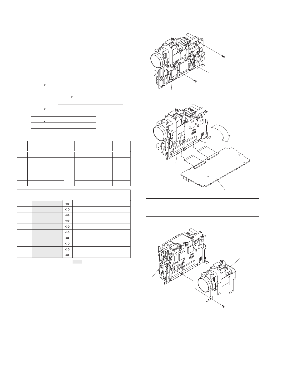
2.3 ASSEMBLY AND DISASSEMBLY OF CAMERA SECTION AND BOARD ASSEMBLY
2.3.1 Disassembly flow chart
This flowchart indicates the disassembly step for the cabinet
parts and board assembly in order to gain access to item(s) to be
serviced. When reassembling, perform the step(s) in reverse or-
der.
NOTE:
Please see Service Manual No. 86700 (MECHANISM ASSY).
2.3.2 Disassembly method
NOTE 2:
As for disassembly/assembly of [2] OP BLOCK ASSEMBLY,
see 2.6 ASSEMBLY AND DISASSEMBLY OF [2] OP BLOCK
ASSEMBLY.
Fig.D1
Fig.D2
[1]
[2]
MAIN BOARD ASSEMBLY
[5]
CCD BOARD ASSEMBLY
[3]
[4]
PREMDA BOARD ASSEMBLY
MECHANISM ASSEMBLY
OP BLOCK ASSEMBLY
MAIN BOARD ASSEMBLY
OP BLOCK ASSEMBLY
/ CCD BOARD ASSEMBLY
PREMDA BOARD ASSEMBLY
MECHANISM
MAIN CN108
MAIN CN107
MAIN CN111
MAIN CN110
PREMDA CN406
PREMDA CN405
PREMDA CN404
PREMDA CN402
PREMDA CN403
PREMDA CN407
OP BLOCK ASSEMBLY CN501
CCD CN5001
PREMDA CN408
PREMDA CN401
SENSOR -
CAPSTAN MOTOR -
DRUM MOTOR -
HEAD -
LOADING MOTOR -
ROTARY ENCODER -
Fig.D1
Fig.D2
Fig.D3
CN1a,b,2(S1),CN1c,d
S2,L2
2(S3a),L3,SHIELD COVER(PR)
CN3a,b,c,d,e,f,2(S3b)
3(S4),BKT(MECHA)
-
NOTE 2
-
-
[1]
[2]/[5]
[3]
[4]
CN1a
CN1b
CN1c
CN1d
CN3a
CN3b
CN3c
CN3d
CN3e
CN3f
24
20
40
40
16
18
11
8
6
6
STEP
No.
PART
CONN.
No.
Pin No.
CONNECTOR
NOTE
Fig.
No.
POINT
Remove the parts marked in .
ASSEMBLY
1
(S1)
2
(S1)
CN1c
CN1d
CN1a
CN1b
[1]
3
(S2)
L2
[2]
([5])
NOTE[2]
(No.86730)1-11
Fig.D3
4
(S3a)
5
(S3a)
L3
PREMDA BOARD ASSEMBLY
6
(S3b)
7
(S3b)
9
(S4)
0.069N
.
m (0.7kgf
.
cm)
0.078N
.
m (0.8kgf
.
cm)
8
(S4)
(PR)
SHIELD COVER
[4]
BKT(MECHA)
CN3a
CN3b
CN3c
CN3e
CN3f
CN3d
[3]
10
(S4)
1-12 (No.86730)
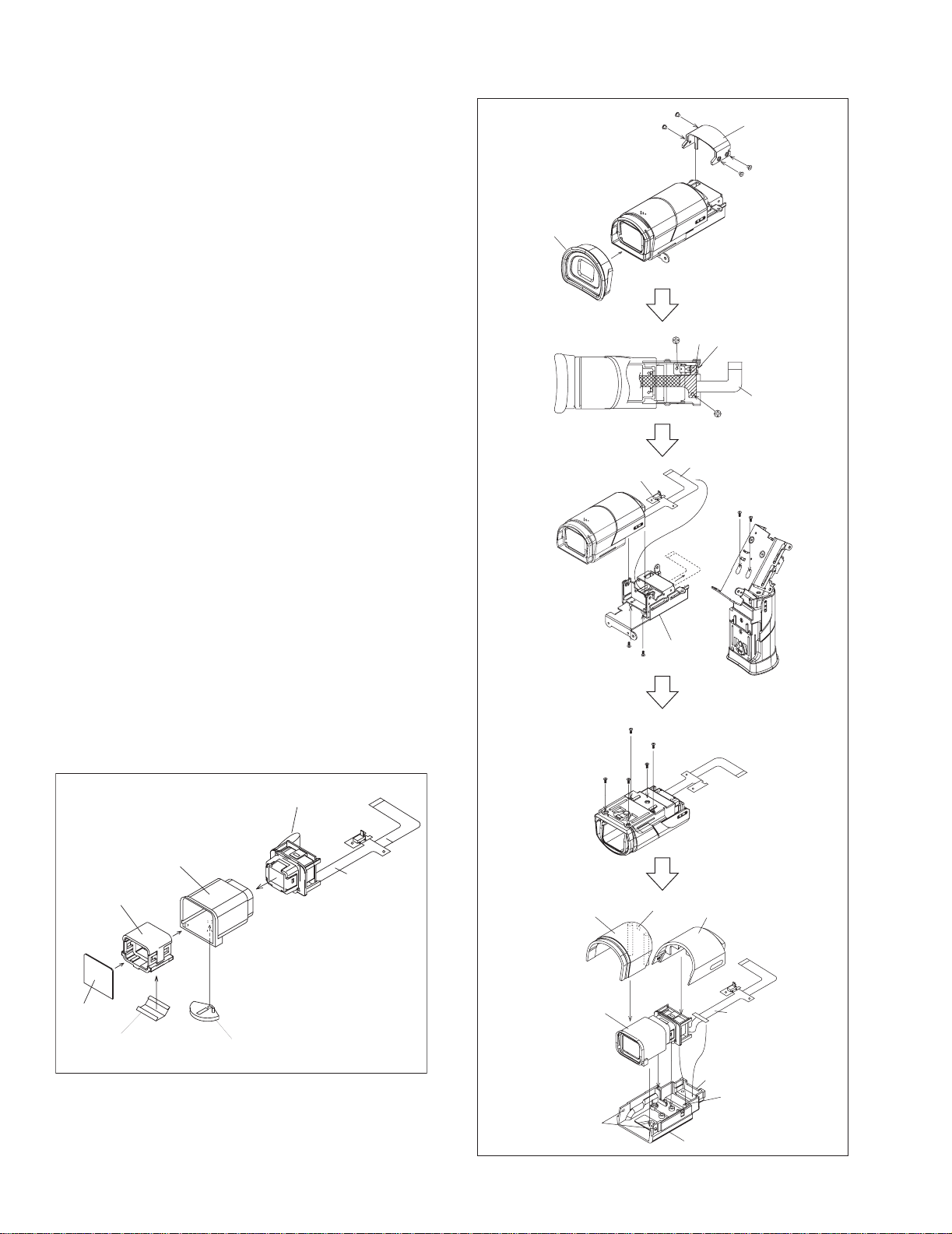
2.4 ASSEMBLY AND DISASSEMBLY OF [8]VF ASSEMBLY
2.4.1 Disassembly of VF ASSEMBLY
(1) Remove the EYE CUP.
(2) Remove the four screws (1 to 4) and then remove the COV-
ER (VF).
(3) Remove the two screws (5 and 6) and then remove the
FPC BOARD from the hook attaching the FPC BOARD.
NOTE 8a:
During the procedure, be careful not to damage the FPC.
When attaching the SW BOARD ASSEMBLY, attach the
SW BOARD ASSEMBLY so that the SW BOARD AS-
SEMBLY comes upwards.
(4) Remove the four screws (7 to 10), and then pull out and re-
move the FPC from the VF HINGE ASSEMBLY.
NOTE 8b:
During the procedure, be careful not to damage the FPC
and the SWITCH.
(5) Remove the five screws (11 to 15).
(6) Remove the UPPER CASE(VF) R.
(7) Remove the UPPER CASE(VF) F and then pull out the
LENS SA and the LCD UNIT ASSEMBLY with the FPC.
NOTE 8c:
In attaching the LCD UNIT ASSEMBLY, put the projec-
tions of the LCD UNIT ASSEMBLY in the slots of the
BOTTOM CASE(VF). Put the STOPPER of the FPC in-
side the BOTTOM CASE(VF). In attaching the UPPER
CASE(VF) F and the UPPER CASE(VF) R, attach the
UPPER CASE(VF) F first and then the UPPER
CASE(VF) R and be careful to keep the FPC inside the
BOTTOM CASE(VF).
2.4.2 Disassembly of the LENS SA
(1) Remove the LEVER(LENS).
(2) Remove the SHEET(LENS).
(3) Remove the LENS ASSEMBLY from the GUIDE
LENS(VF).
NOTE 8d:
Be careful not to lose the SPRING(LENS).
Fig.2-4-2
Fig.2-4-1
SHEET(LENS)
LENS ASSEMBLY
LEVER(LENS)
SPRING(LENS)
NOTE8d:
GUIDE LENS(VF)
LCD UNIT ASSEMBLY
FPC
<LENS SA>
(L8a)
5
(S8b)
6
(S8b)
NOTE8a
FPC
EYE CUP
2
(S8a)
4
(S8a)
3
(S8a)
1
(S8a)
COVER(VF)
EYE CUP
8
(S8a)
7
(S8a)
10
(S8c)
VF HINGE
ASSEMBLY
9
(S8c)
FPC
NOTE8b
12
(S8c)
13
(S8c)
11
(S8c)
15
(S8c)
14
(S8c)
UPPER CASE(VF)F
UPPER CASE(VF)R
LCD UNIT
L8c
ASSEMBLY
NOTE8c
NOTE8c
BOTTOM CASE(VF)
L8b
LENS SA
FPC
(No.86730)1-13
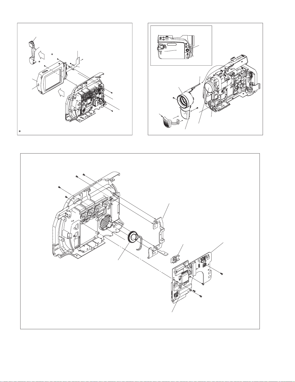
2.5 ASSEMBLY AND DISASSEMBLY OF [10]MONITOR ASSEMBLY (CABINET PARTS)
2.5.1 Disassembly of MONITOR ASSEMBLY (2.5 INCH)
NOTE:
Be careful in removing or handling the monitor assembly, es-
pecially not to soil or scratch the monitor screen during the dis-
assembly procedure.
(1) While removing the four screws (1 to 4) in numerical order
and then disengaging the four hooks (L10a-L10d) in alpha-
betical order, open and remove the MONITOR COVER
ASSEMBLY.
(2) Remove the SENSOR BOARD ASSEMBLY from the
MONITOR CASE.
(3) Disconnect the FPC in the connectors CN10a and CN10b
in this order, and then remove the MONI.HINGE ASSEM-
BLY.
(4) Disconnect the FPC of the LCD MODULE from the connec-
tor CN10c.
(5) Remove one screw (5) and then remove the BL BOARD
ASSEMBLY together with the BACK LIGHT ASSEMBLY.
NOTE 10a:
It depends on the inch size of the monitor assembly
whether the backlight is supplied as an assembly or as
separated parts.
In replacing the backlight assembly, see the Parts List.
NOTE 10b:
Since the BACK LIGHT ASSEMBLY is soldered to the
BL BOARD ASSEMBLY, the BACK LIGHT should not be
separated from the BL BOARD ASSEMBLY except
when replacing them.
(6) Remove the DIFF.SHEET.
(7) Remove the LCD FRAME together with the LCD MODULE.
(8) Remove the SHIELD CASE.
Fig.2-5-1
DIFF. SHEET
NOTE10a
BACK LIGHT
NOTE10b
BL-2.5 BOARD
ASSEMBLY
MONITOR
CASE
L10g
SHIELD CASE
L10f
5
(S10a)
L10b
CN10b
SD10b
SD10a
L10e
CN10a
CN10c
L10a
L10d
L10c
MONITOR COVER
ASSEMBLY
4
(S10b)
3
(S10b)
1
(S10a)
2
(S10a)
b
LCD FRAME
LCD MODULE
c
b
MONI.HINGE
ASSEMBLY
SENSOR BOARD
ASSEMBLY
:0.069N
.
m (0.7kgf
.
cm)
:0.098N
.
m (1.0kgf
.
cm)
a
a
c
1-14 (No.86730)
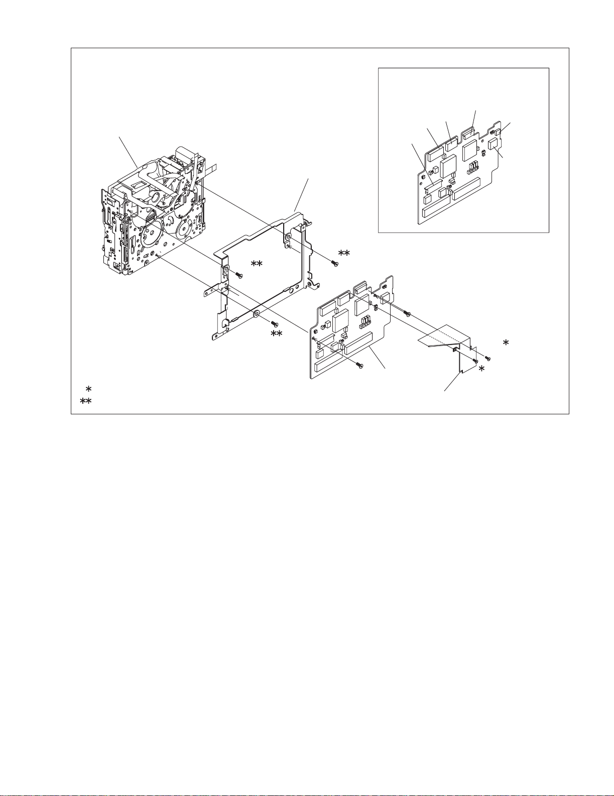
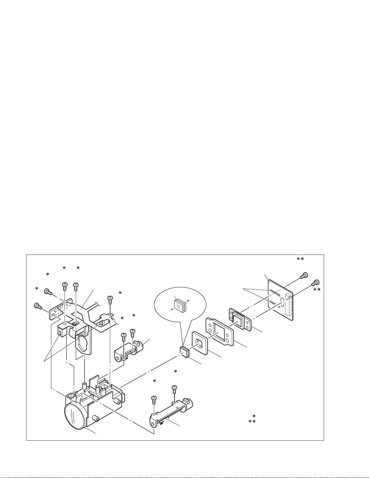
2.6 ASSEMBLY AND DISASSEMBLY OF [2]OP BLOCK ASSEMBLY
/ CCD BOARD ASSEMBLY (CAMERA SECTION AND BOARD ASSEMBLY)
2.6.1 Precautions
(1) Take care in handling the CCD IMAGE SENSOR, OP LPF
and lens components when performing maintenance etc.,
especially with regard to surface contamination, attached
dust or scratching. If fingerprints are present on the surface
they should be wiped away using either a silicon paper,
clean chamois or the cleaning cloth.
(2) The CCD IMAGE SENSOR may have been shipped with a
protective sheet attached to the transmitting glass. When
replacing the CCD IMAGE SENSOR, do not peel off this
sheet from the new part until immediately before it is
mounted in the OP BLOCK ASSEMBLY.
(3) The orientation of the OP LPF is an important factor for
installation. If there is some marking on the OP LPF, be
sure to note it down before removing and to reassemble it
very carefully as it was referring to the marking.
2.6.2 Disassembly of CCD BOARD ASSEMBLY and CCD
BASE ASSEMBLY
(1) Unsolder the CCD BOARD ASSEMBLY by the 14 points
(SD2) and then remove it.
(2) Remove the two screws (1, 2) and remove the CCD BASE
ASSEMBLY.
(3) Remove the SPACER.
(4) Remove the SHEET.
(5) Remove the OP LPF.
2.6.3 Assembly of CCD BASE ASSEMBLY and CCD
BOARD ASSEMBLY
(1) Set the OP LPF to the OP BLOCK ASSEMBLY so that the
OP side touches the OP BLOCK ASSEMBLY.
NOTE 2a:
Pay careful attention to the orientation of the OP LPF.
(2) Set the SHEET to the OP LPF not to come off the right
position.
(3) Attach the SPACER to the OP BLOCK ASSEMBLY.
(4) Fasten them together with the two screws (1, 2).
(5) Set the CCD BOARD ASSEMBLY in the CCD BASE
ASSEMBLY, and then solder it by the 14 points (SD2).
2.6.4 Replacement of service repair parts
The service repair parts for the OP BLOCK ASSEMBLY are as
listed below.
Before replacement of these parts, remove the BRACKET (OP
BLOCK ASSEMBLY) as required.
Take special care not to disconnect any of the FPC wires or
cause any damage due to soldering (excessive heating).
(1) FOCUS MOTOR
(2) ZOOM MOTOR
(3) IRIS MOTOR UNIT
NOTE 2b:
When replacing the FOCUS MOTOR or the ZOOM MOTOR,
solder the FPC at a space of about 1 mm above the terminal
pin.
NOTE 2c:
The IRIS MOTOR UNIT includes the FPC ASSEMBLY and
two sensors.
Fig.2-6-1
2
(S2a)
1
(S2a)
(SD2)
OP
side
CCD
side
Blue
<NOTE 2a>
OP LPF
OP BLOCK
ZOOM MOTOR
<NOTE 2b>
SHEET
OP LPF
SPACER
CCD BASE ASSEMBLY
CCD BAORD
ASSEMBLY
SENSOR
IRIS MOTOR UNIT
<NOTE 2b, c>
FOCUS MOTOR
<NOTE 2b>
0.078N
.
m (0.8kgf
.
cm)
0.118N
.
m (1.2kgf
.
cm)
4
(S2b)
3
(S2b)
6
(S2b)
5
(S2b)
10
(S2b)
11
(S2b)
9
(S2b)
7
(S2c)
8
(S2c)
(No.86730)1-15
2.7 SERVICE NOTE
Use the following chart to manage screws
[1]
1 2 3 4 5 6 7 8 9 10 11 12 13 14 15 16 17 18 19 20 21 22 23 24 25 26 27
C1
C2-4C2-1
2-4-1
2-5-1
2-6-1
C2-2 C2-3
[11] ([12])[2] ([8]-[12]) [8] [10][9]
28 29 30 31 32 33 34 35 36 37 38
C4
[3] [4] [5] [6] [7]
C3
[2]
12345678910
D2 D3
[1] [3] [4]
D1
[8]
1 2 3 4 5 6 7 8 9 10 11 12 13 14 15
[2]/[5]
1234567891011
12345
[10]
Symbol No.
Removing order of screw
Place to stick screw
Screw tightening torque
Reference drawing (Fig.No.)
Screw tightening torque
Reference drawing (Fig.No.)
Reference drawing (Fig.No.)
Reference drawing (Fig.No.)
Screw tightening torque
Screw tightening torque
Symbol No.
Removing order of screw
Place to stick screw
Symbol No.
Symbol No.
Removing order of screw
Place to stick screw
Reference drawing (Fig.No.)
Screw tightening torque
Symbol No.
Removing order of screw
Place to stick screw
<MONITOR ASSEMBLY>
Removing order of screw
Place to stick screw
Reference drawing (Fig.No.)
Screw tightening torque
Symbol No.
Removing order of screw
Place to stick screw
<NOTE>
<OP BLOCK ASSEMBLY>
<VF ASSEMBLY>
<CAMERA AND BOARD ASSEMBLY>
<CABINET PART>
: 0.088N
.
m (0.9kgf
.
cm)
: 0.147N
.
m (1.5kgf
.
cm)
㸉
: 0.078N
.
m (0.8kgf
.
cm)
: 0.098N
.
m (1.0kgf
.
cm)
: 0.069N
.
m (0.7kgf
.
cm)
: 0.118N
.
m (1.2kgf
.
cm)
㸌
1-16 (No.86730)
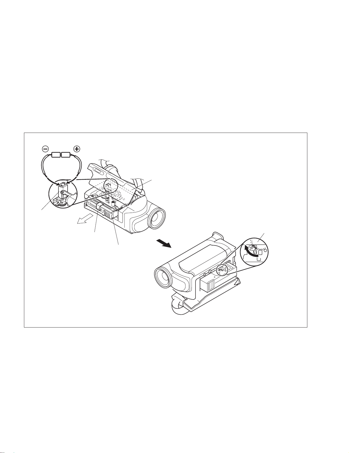
2.8 TAKE OUT CASSETTE TAPE
NOTE :
The following procedure describes a simplified method of
ejecting the cassette tape in case it is not possible to eject it,
due to an electrical failure.
Be careful not to damage any of the parts or the tape when per-
forming repairs or maintenance work.
(1) Remove the Power Unit (battery, DC code, etc.) from the
set.
(2) Open the CASSETTE COVER.
(3) Attach a piece of PVC TAPE at the front of the CASSETTE
HOUSING ASSEMBLY.
NOTE:
This helps prevent the tape from being damaged when
the CASSETTE HOUSING ASSEMBLY is moved up-
ward at the unloading end.
(4) Apply DC 3V to the electrode on the top surface of the
LOADING MOTOR ASSEMBLY to set the MECHANISM
ASSEMBLY to the EJECT mode.
Unloading end is EJECT mode.
(5) If there is any slack tape in the tape transport system, wind
it inside the DVC CASSETTE TAPE by turning the REEL
DISK ASSEMBLY (SUP) from the backside of the SLIDE
DECK ASSEMBLY.
(6) Peel off the PVC TAPE and take out the DVC CASSETTE
TAPE from the CASSETTE HOUSING ASSEMBLY.
NOTE:
Make sure that grease or a similar substance is not at-
tached to the surface of the tape.
Similarly, also make sure that grease or a similar sub-
stance is not attached on the MECHANISM ASSEMBLY.
Fig.2-8-1
REEL DISK ASSEMBLY (SUP)
(DC3V)
PVC T
LOADING MOTOR
ASSEMBLY
APE
CASSETTE HOUSING
ASSEMBLY
CASSETTE COVER

(No.86730)1-17
2.9 EMERGENCY DISPLAY
Whenever some abnormal signal is input to the syscon CPU, an
error number (E01, as an example) is displayed on the LCD mon-
itor or (in the electronic view finder).
In every error status, such the message as shown below alter
nately appear over and over.
• In an emergency mode, all operations except turning on/off the
POWER switch are ineffectual.
Example (in case of the error number E01):
Fig.2-9-1
E01
UNIT IN
SAFEGUARD MODE
E01
REMOVE AND
REATTACH BATTERY
LCD
display
Emergency
mode
Details Possible cause
E01 LOADING In the case the encoder posi-
tion is not shifted to the next
point though the loading motor
has rotated in the loading direc-
tion for 4 seconds or more. This
error is defined as [E01].
1. The mechanism is locked during mode shift.
2. The mechanism is locked at the mechanism loading end,
because the encoder position is skipped during mechanism
mode shift.
3. No power is supplied to the loading MDA.
E02 UNLOADING In the case the encoder posi-
tion is not shifted to the next
point though the loading motor
has rotated in the unloading di-
rection for 4 seconds or more.
This error is defined as [E02].
1. The mechanism is locked during mode shift.
2. The mechanism is locked at the mechanism loading end,
because the encoder position is skipped during mechanism
mode shift.
E03 TU & SUP REEL FG In the case no REEL FG is pro-
duced for 4 seconds or more in
the capstan rotation mode after
loading was complete, the
mechanism mode is shifted to
STOP with the pinch roller set
off. This error is defined as
[E03].
However, no REEL EMG is de-
tected in the SLW/STILL mode.
1. The idler gear does not engage with the reel disk well.
2. Though the idler gear and reel disk are engaged with each
other, the tape is not wound because of overload to the
mechanism.
3. No FG pulse is output from the reel sensor.
4. No power is supplied to the reel sensor.
5. Tape transport operation takes place with a cassette having
no tape inside.
6. The tape slackens and no pulse is produced until the slack
is taken up and the tape comes into the normal status.
E04 DRUM FG In the case there is no DRUM
FG input in the drum rotation
mode for 4 seconds or more.
This error is defined as [E04],
and the mechanism mode is
shifted to STOP with the pinch
roller set off.
1. The drum cannot be started or drum rotation is stopped be-
cause tape transport load is too high.
1) Tape tension is extremely high.
2) The tape is damaged or soiled with grease, etc.
2. The DRUM FG signal is not received by the syscon CPU.
1) Disconnection in the middle of the signal line.
2) Failure of the DRUM FG pulse generator (hall element).
3. No drum control voltage is supplied to the MDA.
4. No power is supplied to the DRUM MDA.
E05 - - -
E06 CAPSTAN FG In the case no CAPSTAN FG is
produced in the capstan rota-
tion mode for 2 seconds or
more. This error is defined as
[E06], and the mechanism
mode is shifted to STOP with
the pinch roller set off.
However, no CAPSTAN EMG
is detected in the STILL/FF/
REW mode.
1. The CAPSTAN FG signal is not received by the syscon
CPU.
1) Disconnection in the middle of the signal line.
2) Failure of the CAPSTAN FG pulse generator (MR ele-
ment).
2. No capstan control voltage is supplied to the MDA.
4. The capstan cannot be started or capstan rotation is
stopped because tape transport load is too high.
1) Tape tension is extremely high. (Mechanical locking)
2) The tape is damaged or soiled with grease, etc. (Tape
tangling occurs, etc.)
1-18 (No.86730)
SECTION 3
ADJUSTMENT
3.1 PREPARATION
(1) Precaution
This model does not contain adjustment controls (VR).
General deck system, camera system and monitor system
adjustment are not required. However, if MAIN board need
replacement, please use original EEP ROM on to new
board. Then adjustment are not required. And if parts such
as the following need replacement, special computerized
adjustment are required. 3.5.1 Electrical adjustment with
personal computer is setup and it adjusts using a service
support system. Please contact to JVC Service for detail in-
formation.
• OP BLOCK ASSEMBLY
• EEP ROM (IC1005 of MAIN board)
• MONITOR / VF ASSEMBLY
In the event of malfunction with electrical circuits, trouble-
shooting with the aid of proper test instruments most be
done first, and then commence necessary repair, replace-
ment and adjustment, etc.
a) In case of wiring to chip test points for measurement,
use IC clips, etc. to avoid any stress.
b) Since connectors are fragile, carefully handle them in
disconnecting and connecting.
c) Short circuit between operation unit and DECK chas-
sis.
(2) Required test equipment
a) Color TV monitor.
b) AC power adapter
c) Oscilloscope (dual-trace type, observable 100 MHz
or higher frequency)
• It is recommended to use one observable 300 MHz
or higher frequency.
d) Digital voltmeter
e) Frequency counter (with threshold level adjuster)
f) Personal computer
3.2 TOOLS REQUIRED FOR ADJUSTMENT
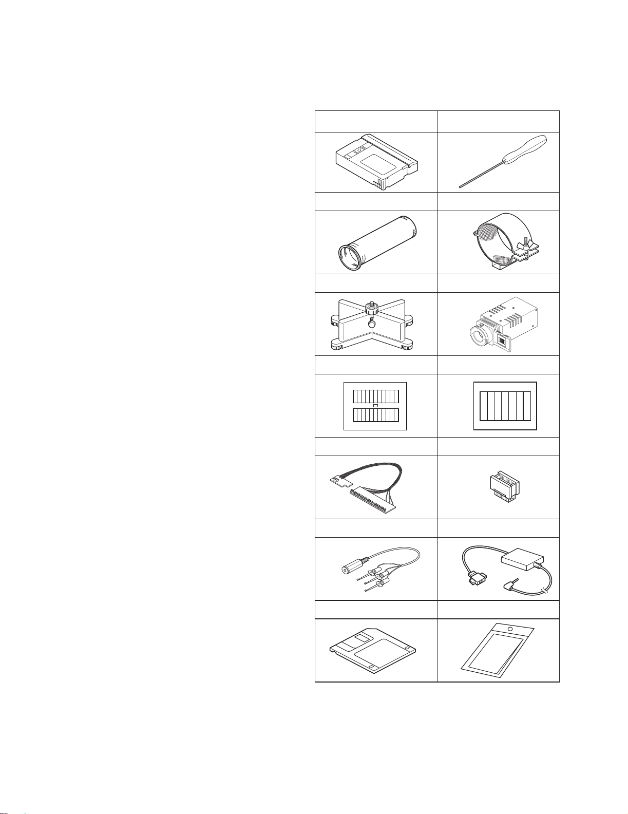
Fig.3-2-1
1
Alignment tape
MC-2
3
INF adjustment lens
YTU92001B
7
Gray scale chart
YTU94133A
8
Color bar chart
YTU94133C
4
INF lens holder
YTU94087
6
Light box assembly
YTU93096A
5
Camera stand
YTU93079
13
Service support system
YTU94057-67
14
Cleaning cloth
KSMM-01
12
PC cable
QAM0099-005
11
Communication cable
YTU93107A
9
Jig connector cable
YTU93106B
10
Extension connector
YTU94145C-30
2
Guide driver (Hexagonal)
D-770-1.27
 Loading...